How to Address Leakage Current in PNP Transistor Applications?
JUL 28, 202510 MIN READ
Generate Your Research Report Instantly with AI Agent
Patsnap Eureka helps you evaluate technical feasibility & market potential.
PNP Transistor Leakage Current Background and Objectives
PNP transistors have been a fundamental component in electronic circuits since their inception in the mid-20th century. These devices play a crucial role in various applications, from simple amplifiers to complex integrated circuits. However, one of the persistent challenges in PNP transistor applications has been the issue of leakage current, which can significantly impact the performance and efficiency of electronic systems.
Leakage current in PNP transistors refers to the undesired flow of current through the device when it is supposed to be in an off state. This phenomenon occurs due to various factors, including temperature variations, material impurities, and device geometry. As electronic devices continue to shrink in size and increase in complexity, addressing leakage current has become increasingly important to maintain optimal performance and energy efficiency.
The evolution of PNP transistor technology has been marked by continuous efforts to mitigate leakage current issues. Early designs focused primarily on improving manufacturing processes and material purity to reduce inherent leakage. As the semiconductor industry progressed, more sophisticated techniques emerged, such as advanced doping profiles and novel device structures, aimed at minimizing leakage pathways within the transistor.
In recent years, the demand for low-power electronics, particularly in mobile and IoT devices, has intensified the focus on leakage current reduction. This trend has driven research into innovative transistor designs and materials that can offer better control over leakage mechanisms. Additionally, the rise of high-performance computing and data centers has highlighted the need for more efficient transistors to manage power consumption and heat generation in large-scale systems.
The primary objective in addressing leakage current in PNP transistor applications is to develop solutions that can effectively minimize unwanted current flow without compromising the device's intended functionality. This goal encompasses several key aspects, including enhancing the transistor's off-state characteristics, improving thermal stability, and optimizing overall power efficiency.
Researchers and engineers in the field are exploring multifaceted approaches to tackle this challenge. These include investigating novel semiconductor materials with superior insulating properties, developing advanced transistor architectures that provide better electrostatic control, and implementing innovative circuit design techniques to compensate for leakage effects.
As we delve deeper into the technical aspects of leakage current in PNP transistors, it is essential to consider the broader implications for the electronics industry. Successful strategies for mitigating leakage current have the potential to enable more energy-efficient devices, extend battery life in portable electronics, and contribute to the overall reduction of power consumption in electronic systems worldwide.
Market Demand for Low-Leakage PNP Transistors
The market demand for low-leakage PNP transistors has been steadily increasing in recent years, driven by the growing need for energy-efficient electronic devices and systems. This demand is particularly pronounced in sectors such as portable electronics, IoT devices, and automotive applications, where power consumption and battery life are critical factors.
In the consumer electronics market, manufacturers are constantly striving to extend the battery life of smartphones, tablets, and wearable devices. Low-leakage PNP transistors play a crucial role in reducing standby power consumption, which directly impacts the overall energy efficiency of these devices. As consumers increasingly prioritize longer-lasting batteries, the demand for components that minimize power loss continues to rise.
The Internet of Things (IoT) sector represents another significant driver for low-leakage PNP transistors. With the proliferation of connected devices in smart homes, industrial automation, and environmental monitoring, there is a growing need for sensors and actuators that can operate for extended periods on limited power sources. Low-leakage transistors are essential in designing ultra-low-power circuits for these applications, enabling longer deployment times and reducing maintenance costs.
In the automotive industry, the shift towards electric and hybrid vehicles has intensified the focus on power management and efficiency. Low-leakage PNP transistors are vital components in various automotive systems, including battery management, power distribution, and sensor networks. As vehicles become more electrified and incorporate advanced driver assistance systems (ADAS), the demand for high-performance, low-power semiconductors continues to expand.
The medical device sector also contributes to the market demand for low-leakage PNP transistors. Implantable medical devices, such as pacemakers and insulin pumps, require extremely low power consumption to ensure long-term operation without frequent battery replacements. The use of low-leakage transistors in these devices is crucial for patient safety and comfort.
Market analysts project that the global demand for low-leakage transistors, including PNP types, will continue to grow at a compound annual growth rate (CAGR) of 6-8% over the next five years. This growth is attributed to the increasing adoption of IoT devices, the expansion of 5G networks, and the ongoing trend towards miniaturization and power efficiency in electronic products.
Semiconductor manufacturers are responding to this demand by investing in research and development to further reduce leakage currents in PNP transistors. Advanced fabrication techniques, such as silicon-on-insulator (SOI) technology and high-k dielectrics, are being explored to minimize parasitic effects and improve overall transistor performance. These innovations are expected to drive the next generation of low-leakage PNP transistors, meeting the evolving needs of various industries and applications.
Current Challenges in PNP Transistor Leakage Mitigation
PNP transistor leakage current remains a significant challenge in modern electronic design, particularly in applications requiring high precision and low power consumption. The primary issue stems from the inherent characteristics of PNP transistors, which are prone to unwanted current flow even when in their "off" state. This leakage can lead to increased power consumption, reduced battery life in portable devices, and compromised performance in sensitive analog circuits.
One of the main factors contributing to leakage current in PNP transistors is temperature sensitivity. As ambient temperature rises, the leakage current tends to increase exponentially, potentially leading to thermal runaway in extreme cases. This temperature dependence makes it particularly challenging to design stable circuits for applications that operate across a wide temperature range.
Another significant challenge is the trade-off between leakage current and switching speed. Attempts to reduce leakage often result in slower switching times, which can be problematic in high-frequency applications. Engineers must carefully balance these competing requirements, often resorting to complex circuit designs or advanced fabrication techniques to achieve optimal performance.
The miniaturization of semiconductor devices has also exacerbated the leakage current issue. As transistor sizes shrink, the relative impact of leakage current becomes more pronounced. This is particularly evident in sub-micron technologies, where quantum effects begin to play a significant role in device behavior.
Surface leakage is another concern, especially in high-voltage applications. Impurities or defects on the semiconductor surface can create conductive paths, leading to increased leakage. This necessitates careful attention to surface passivation techniques and packaging materials to minimize such effects.
In analog circuit design, leakage current can introduce non-linearities and offset errors, compromising the accuracy of measurements and signal processing. This is particularly problematic in applications such as precision instrumentation, medical devices, and high-resolution data converters.
The variability of leakage current across different transistors, even those on the same chip, poses challenges for circuit matching and uniformity. This variability can lead to unpredictable behavior in differential circuits and mismatch in current mirrors, requiring sophisticated compensation techniques.
Addressing these challenges requires a multifaceted approach, combining innovations in semiconductor materials, device structures, circuit design techniques, and manufacturing processes. Researchers and engineers are exploring various strategies, including the use of high-k dielectrics, advanced doping profiles, and novel transistor architectures to mitigate leakage current while maintaining other desirable characteristics of PNP transistors.
Existing Solutions for PNP Transistor Leakage Reduction
01 Leakage current reduction techniques
Various techniques are employed to reduce leakage current in PNP transistors. These include optimizing the transistor structure, improving isolation between components, and implementing advanced manufacturing processes. Such techniques help minimize unwanted current flow and improve overall transistor performance.- Leakage current reduction techniques: Various techniques are employed to reduce leakage current in PNP transistors. These may include optimizing the transistor structure, improving isolation between components, and implementing advanced manufacturing processes. Such techniques aim to minimize unwanted current flow when the transistor is in its off state, thereby improving overall device performance and efficiency.
- Temperature compensation for leakage current: Temperature compensation methods are used to mitigate the effects of leakage current in PNP transistors across different operating temperatures. These techniques may involve the use of additional circuitry or specialized design approaches to maintain consistent performance and minimize leakage current variations due to temperature changes.
- Leakage current measurement and characterization: Accurate measurement and characterization of leakage current in PNP transistors are crucial for device optimization and quality control. Various methods and circuits are developed to precisely measure and analyze leakage current under different operating conditions, enabling better understanding and management of this parameter in transistor design and manufacturing.
- Leakage current in power management applications: In power management applications, controlling leakage current in PNP transistors is essential for improving energy efficiency and battery life. Specialized circuit designs and control techniques are implemented to minimize leakage current in power management ICs and voltage regulators that utilize PNP transistors.
- Leakage current in memory devices: Leakage current in PNP transistors used in memory devices can affect data retention and power consumption. Various design strategies and circuit techniques are employed to minimize leakage current in memory cells and peripheral circuits, ensuring reliable operation and reduced standby power consumption in memory applications.
02 Temperature compensation for leakage current
Temperature variations can significantly affect leakage current in PNP transistors. Implementing temperature compensation circuits or techniques helps maintain stable transistor performance across different operating temperatures, ensuring consistent leakage current levels.Expand Specific Solutions03 Leakage current measurement and testing
Accurate measurement and testing of leakage current in PNP transistors are crucial for quality control and performance optimization. Specialized testing methods and equipment are used to precisely quantify leakage current under various operating conditions.Expand Specific Solutions04 Circuit design for leakage current mitigation
Innovative circuit designs can help mitigate leakage current issues in PNP transistors. These designs may include feedback loops, compensation networks, or specialized biasing techniques to minimize unwanted current flow and improve overall circuit performance.Expand Specific Solutions05 Substrate engineering for leakage current control
Modifying the substrate properties and structure of PNP transistors can significantly impact leakage current. Advanced substrate engineering techniques, such as using specialized materials or implementing novel doping profiles, can help control and reduce leakage current in these devices.Expand Specific Solutions
Key Players in PNP Transistor Manufacturing
The leakage current issue in PNP transistor applications is a mature technical challenge within the semiconductor industry. The market for addressing this problem is substantial, given the widespread use of PNP transistors in various electronic devices. Major players like Infineon Technologies, ROHM, and STMicroelectronics are at the forefront of developing solutions, leveraging their extensive experience in semiconductor manufacturing. These companies, along with others such as ON Semiconductor and Renesas Electronics, are continuously innovating to improve PNP transistor performance and reduce leakage current. The competitive landscape is characterized by ongoing research and development efforts, with a focus on advanced materials and novel circuit designs to mitigate leakage effects.
Infineon Technologies AG
Technical Solution: Infineon has developed advanced PNP transistor designs with reduced leakage current using their proprietary RESURF (Reduced Surface Field) technology[1]. This technology optimizes the electric field distribution in the device, minimizing surface-related leakage paths. They have also implemented advanced doping profiles and improved isolation techniques to further reduce leakage currents. Infineon's solutions include the use of buried layers and specialized guard ring structures to minimize parasitic effects and substrate coupling[2]. Additionally, they have introduced innovative packaging solutions that help in thermal management, indirectly contributing to leakage current reduction in high-power applications[3].
Strengths: Proprietary RESURF technology, advanced doping profiles, and specialized packaging solutions. Weaknesses: Potentially higher manufacturing costs due to complex structures and processes.
QUALCOMM, Inc.
Technical Solution: Qualcomm has addressed leakage current in PNP transistors through their advanced process node developments and circuit design techniques. They have implemented FinFET technology in their more recent chip designs, which inherently offers better control over leakage currents due to improved channel control[10]. Qualcomm has also developed advanced power gating techniques and multi-threshold voltage design methodologies to minimize leakage in their complex SoC (System-on-Chip) designs that incorporate PNP transistors[11]. Their approach includes the use of adaptive voltage scaling and dynamic frequency adjustment to optimize power consumption and reduce leakage currents in various operating conditions[12].
Strengths: FinFET technology implementation, advanced power gating techniques, and adaptive voltage/frequency scaling. Weaknesses: Solutions may be more tailored to mobile and wireless applications, potentially limiting applicability in other domains.
Core Innovations in PNP Transistor Design
Apparatus and circuit having reduced leakage current and method therefor
PatentInactiveUS6800908B2
Innovation
- The implementation of diffusion regions within well regions of transistors, which are biased with a higher voltage potential than the current carrying electrodes when the transistors are inactive, creates a reverse bias across the channel region, reducing leakage current and power consumption.
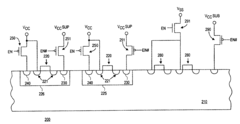
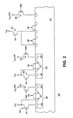
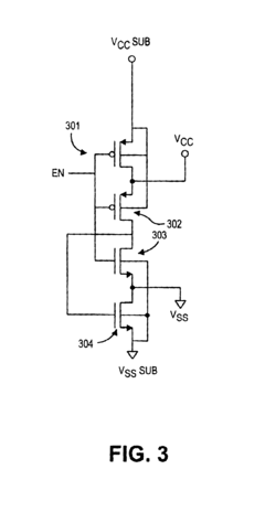
Patent
Innovation
- Implementation of a compensation circuit to minimize leakage current in PNP transistor applications.
- Utilization of temperature-dependent biasing to counteract leakage current variations across different operating conditions.
- Development of a feedback loop system to continuously monitor and correct for leakage current fluctuations.
Thermal Management Strategies for PNP Transistors
Thermal management is a critical aspect of PNP transistor applications, particularly when addressing leakage current issues. Effective thermal strategies can significantly mitigate the impact of leakage current, enhancing overall device performance and reliability. One key approach involves the implementation of heat sinks and thermal pads to dissipate excess heat generated by the transistor during operation. These components facilitate the transfer of thermal energy away from the device, reducing the risk of temperature-induced leakage current increases.
Another crucial strategy is the optimization of circuit board design to improve heat distribution. This includes the use of thermal vias, which are plated through-holes that conduct heat from one layer of a PCB to another, effectively creating thermal pathways to dissipate heat more efficiently. Additionally, the strategic placement of components on the PCB can help minimize thermal hotspots and ensure more uniform heat distribution across the board.
Active cooling methods, such as forced-air cooling or liquid cooling systems, can be employed in high-power applications where passive cooling techniques may be insufficient. These systems actively remove heat from the transistor and surrounding components, maintaining optimal operating temperatures and reducing leakage current. In some cases, thermoelectric coolers (TECs) may be utilized for precise temperature control in sensitive applications.
The selection of appropriate packaging materials and techniques also plays a vital role in thermal management. Advanced packaging solutions, such as flip-chip technology or the use of thermally conductive encapsulants, can significantly improve heat dissipation from the transistor die to the external environment. Furthermore, the integration of temperature sensors and feedback control systems allows for real-time monitoring and adjustment of operating conditions to maintain optimal thermal performance.
Proper thermal simulation and modeling during the design phase are essential for developing effective thermal management strategies. Computational fluid dynamics (CFD) and finite element analysis (FEA) tools enable engineers to predict thermal behavior and optimize designs before physical prototyping. This approach helps identify potential thermal issues early in the development process, reducing the need for costly redesigns and improving overall system reliability.
In conclusion, a comprehensive thermal management strategy for PNP transistors should incorporate a combination of passive and active cooling techniques, optimized circuit design, advanced packaging solutions, and thorough thermal analysis. By addressing thermal concerns effectively, designers can minimize leakage current and enhance the overall performance and longevity of PNP transistor-based applications.
Environmental Impact of PNP Transistor Manufacturing
The manufacturing process of PNP transistors has significant environmental implications that warrant careful consideration. The production of these semiconductor devices involves several stages, each with potential environmental impacts. The primary concerns revolve around resource consumption, energy usage, and the generation of hazardous waste materials.
Raw material extraction and processing form the initial phase of environmental impact. Silicon, the base material for transistors, is typically obtained through mining and refining processes that can lead to land degradation and water pollution. The purification of silicon to semiconductor-grade quality requires substantial energy input, contributing to greenhouse gas emissions. Additionally, the production of dopants such as boron for PNP transistors involves chemical processes that may release harmful byproducts into the environment if not properly managed.
The fabrication of PNP transistors utilizes various chemicals, including photoresists, etchants, and cleaning agents. Many of these substances are toxic and pose risks to both human health and the environment if released. Proper handling, storage, and disposal of these chemicals are crucial to mitigate potential contamination of soil and water resources. Furthermore, the etching processes used in transistor manufacturing often employ hydrofluoric acid and other corrosive substances, which require stringent safety measures and specialized waste treatment facilities.
Water consumption is another significant environmental concern in PNP transistor production. The manufacturing process requires large volumes of ultra-pure water for cleaning and rinsing operations. This not only strains local water resources but also generates wastewater that must be treated before release. The treatment of this wastewater is energy-intensive and may involve the use of additional chemicals, further compounding the environmental footprint of the manufacturing process.
Energy usage throughout the production cycle contributes substantially to the overall environmental impact. Clean room facilities, essential for maintaining the sterile conditions required for semiconductor manufacturing, consume significant amounts of electricity for air filtration, temperature control, and humidity regulation. The operation of high-precision equipment and the various thermal processes involved in transistor fabrication also demand considerable energy input, often relying on fossil fuel-based power sources.
The disposal and recycling of electronic waste containing PNP transistors present long-term environmental challenges. As consumer electronics become obsolete at an increasing rate, the proper handling of discarded devices is crucial to prevent the leaching of harmful substances into ecosystems. The presence of lead, cadmium, and other toxic materials in older transistors and associated components necessitates specialized recycling processes to recover valuable materials and safely dispose of hazardous elements.
To address these environmental concerns, the semiconductor industry has been implementing various sustainability initiatives. These include the adoption of more energy-efficient manufacturing technologies, the development of less toxic chemical alternatives, and the implementation of closed-loop water recycling systems. Additionally, efforts are being made to improve the recyclability of electronic components and to reduce the overall material footprint of transistor production.
Unlock deeper insights with Patsnap Eureka Quick Research — get a full tech report to explore trends and direct your research. Try now!
Generate Your Research Report Instantly with AI Agent
Supercharge your innovation with Patsnap Eureka AI Agent Platform!