How to Utilize PNP Transistors for Advanced Signal Conditioning?
JUL 28, 20259 MIN READ
Generate Your Research Report Instantly with AI Agent
Patsnap Eureka helps you evaluate technical feasibility & market potential.
PNP Transistor Fundamentals and Objectives
PNP transistors have been a cornerstone in electronic circuit design since their inception in the mid-20th century. These devices, characterized by their ability to control current flow based on input signals, have played a crucial role in the evolution of signal conditioning techniques. The fundamental principle of PNP transistors lies in their structure, consisting of a thin base region sandwiched between two P-type semiconductor layers. This configuration allows for the control of current flow from the emitter to the collector when a small current is applied to the base.
In the context of advanced signal conditioning, PNP transistors offer unique advantages that make them indispensable in modern electronic systems. Their ability to operate as current-controlled current sources makes them particularly useful in applications requiring precise current regulation and amplification. This characteristic is essential in various signal conditioning scenarios, such as in sensor interfaces, where weak signals need to be amplified without introducing significant noise or distortion.
The objectives of utilizing PNP transistors in advanced signal conditioning are multifaceted. Primarily, they aim to enhance signal quality by improving signal-to-noise ratios, reducing distortion, and increasing linearity in analog circuits. PNP transistors are also employed to achieve better temperature stability and wider dynamic range in signal processing applications. These objectives align with the growing demand for high-performance, low-power electronic systems in industries ranging from telecommunications to medical devices.
As technology progresses, the role of PNP transistors in signal conditioning continues to evolve. Recent advancements have focused on optimizing transistor characteristics for specific applications, such as high-frequency operations or ultra-low-power designs. The integration of PNP transistors with complementary NPN devices in bipolar and BiCMOS technologies has opened new avenues for complex signal conditioning circuits, enabling more sophisticated analog and mixed-signal processing capabilities.
The ongoing development of PNP transistor technology is driven by the need for improved performance in emerging applications. This includes the pursuit of higher bandwidth, lower noise figures, and enhanced linearity for next-generation communication systems. Additionally, there is a growing emphasis on developing PNP transistors suitable for extreme environment operations, such as in aerospace and automotive applications, where reliability under harsh conditions is paramount.
Understanding the fundamentals and objectives of PNP transistor utilization in advanced signal conditioning is crucial for engineers and researchers aiming to push the boundaries of electronic system design. As we look towards future technological advancements, the continued refinement and innovative application of PNP transistors will undoubtedly play a significant role in shaping the landscape of signal processing and conditioning techniques.
Market Demand Analysis for PNP-based Signal Conditioning
The market demand for PNP-based signal conditioning solutions has been steadily growing, driven by the increasing need for precise and reliable signal processing across various industries. The global signal conditioning market, which includes PNP transistor applications, is projected to reach significant growth in the coming years, with a compound annual growth rate (CAGR) exceeding industry averages.
One of the primary factors fueling this demand is the rapid expansion of industrial automation and control systems. As manufacturing processes become more sophisticated, the requirement for accurate signal conditioning to ensure optimal performance of sensors and actuators has intensified. PNP transistors, known for their ability to handle small current amplification and voltage regulation, are increasingly being integrated into these systems to enhance signal quality and reliability.
The automotive sector represents another substantial market for PNP-based signal conditioning. With the rise of electric and autonomous vehicles, there is a growing need for advanced sensor systems that can provide precise data for vehicle control and safety features. PNP transistors play a crucial role in conditioning signals from various automotive sensors, contributing to improved vehicle performance and safety.
In the healthcare industry, the demand for PNP-based signal conditioning is also on the rise. Medical devices and diagnostic equipment require highly accurate signal processing to ensure reliable patient monitoring and treatment. PNP transistors are utilized in these applications to amplify and condition weak bioelectric signals, enabling more accurate diagnoses and treatment decisions.
The telecommunications sector is another key driver of market demand for PNP-based signal conditioning. As 5G networks continue to expand, there is an increasing need for high-performance signal processing components to manage the complex RF signals involved in wireless communications. PNP transistors are employed in various stages of signal amplification and conditioning within telecom infrastructure.
The aerospace and defense industries also contribute significantly to the market demand. These sectors require robust and reliable signal conditioning solutions for applications such as radar systems, avionics, and satellite communications. PNP transistors are valued for their ability to operate in harsh environments and provide stable signal amplification under varying conditions.
Looking at regional trends, Asia-Pacific is expected to witness the highest growth rate in the PNP-based signal conditioning market. This is primarily due to the rapid industrialization in countries like China and India, coupled with increasing investments in automation and smart manufacturing initiatives. North America and Europe continue to be significant markets, driven by technological advancements and the presence of key industry players.
Current Challenges in PNP Transistor Applications
Despite the widespread use of PNP transistors in signal conditioning applications, several challenges persist in their implementation and optimization. One of the primary issues is the inherent slower switching speed compared to their NPN counterparts. This limitation arises from the minority carrier transport mechanism in PNP transistors, which results in longer turn-on and turn-off times. Consequently, this restricts their use in high-frequency applications and can lead to signal distortion in certain conditioning scenarios.
Another significant challenge is the temperature sensitivity of PNP transistors. As ambient temperature fluctuates, the transistor's characteristics, such as current gain and leakage current, can vary substantially. This temperature dependence can introduce errors in signal conditioning circuits, particularly in precision applications where stability is crucial. Designers must implement complex compensation techniques to mitigate these thermal effects, adding to the overall circuit complexity and cost.
Power consumption remains a concern in PNP transistor applications, especially in battery-operated or low-power devices. PNP transistors typically exhibit higher collector-emitter saturation voltage (VCE(sat)) compared to NPN transistors, resulting in increased power dissipation. This characteristic can limit the efficiency of signal conditioning circuits and pose challenges in thermal management, particularly in compact or densely packed designs.
Noise performance is another area where PNP transistors face challenges. The inherent noise characteristics of PNP devices, including shot noise and flicker noise, can degrade signal quality in sensitive analog circuits. This is particularly problematic in low-level signal conditioning applications, where maintaining a high signal-to-noise ratio is critical for accurate measurements and data acquisition.
The limited availability of high-performance PNP transistors compared to their NPN counterparts poses challenges for designers seeking optimal solutions. Many semiconductor manufacturers focus more on developing advanced NPN devices, leaving fewer options for high-specification PNP transistors. This scarcity can lead to compromises in circuit design or the need for more complex solutions to achieve desired performance levels.
Lastly, the asymmetry between PNP and NPN transistors in complementary circuits presents design challenges. Achieving perfectly matched characteristics between PNP and NPN devices is difficult, leading to potential imbalances in circuit operation. This asymmetry can result in issues such as offset voltages, gain mismatches, and distortion in differential amplifiers and other precision analog circuits.
Existing PNP Signal Conditioning Solutions
01 PNP transistor structure and fabrication
This category focuses on the design and manufacturing processes of PNP transistors. It includes innovations in transistor structure, such as vertical and lateral PNP configurations, as well as methods for fabricating these devices on semiconductor substrates. These advancements aim to improve transistor performance, reduce size, and enhance integration with other circuit components.- PNP transistor structure and fabrication: This category focuses on the design and manufacturing processes of PNP transistors. It includes innovations in transistor structure, such as vertical and lateral PNP configurations, as well as methods for fabricating these devices on semiconductor substrates. These advancements aim to improve the performance and efficiency of PNP transistors for signal conditioning applications.
- Signal amplification and conditioning circuits: This category covers various circuit designs that utilize PNP transistors for signal amplification and conditioning. These circuits may include differential amplifiers, current mirrors, and other configurations that leverage the characteristics of PNP transistors to process and enhance signals. The designs aim to improve signal-to-noise ratio, bandwidth, and overall performance in analog and mixed-signal applications.
- Temperature compensation and biasing techniques: This category addresses methods and circuits for temperature compensation and biasing of PNP transistors in signal conditioning applications. These techniques aim to maintain stable performance across varying temperature conditions and ensure proper operating points for the transistors. Innovations in this area may include bandgap reference circuits, current sources, and other compensation schemes.
- Integration with other semiconductor devices: This category focuses on the integration of PNP transistors with other semiconductor devices in signal conditioning circuits. It includes the development of BiCMOS technologies, which combine bipolar transistors (including PNP) with CMOS devices on a single chip. These integrated solutions aim to leverage the strengths of different device types to achieve optimal performance in signal processing applications.
- Noise reduction and signal isolation techniques: This category covers methods and circuit designs for reducing noise and improving signal isolation in PNP transistor-based signal conditioning applications. It includes techniques such as chopper stabilization, guard rings, and other isolation structures to minimize interference and improve the overall signal quality. These innovations aim to enhance the accuracy and reliability of signal processing in sensitive analog circuits.
02 Signal conditioning circuits using PNP transistors
This category covers various signal conditioning circuits that utilize PNP transistors. These circuits are designed to process and manipulate input signals, such as amplification, filtering, and level shifting. The use of PNP transistors in these circuits can provide advantages in terms of input impedance, current sourcing capabilities, and complementary designs when used alongside NPN transistors.Expand Specific Solutions03 Temperature compensation and biasing techniques
This category addresses methods for temperature compensation and biasing in circuits using PNP transistors. These techniques aim to maintain stable operation across varying temperature conditions and ensure proper biasing for optimal performance. Innovations in this area include the use of matched transistor pairs, bandgap reference circuits, and adaptive biasing schemes.Expand Specific Solutions04 Integration of PNP transistors in analog and mixed-signal circuits
This category focuses on the integration of PNP transistors in complex analog and mixed-signal circuits. It covers applications such as operational amplifiers, comparators, analog-to-digital converters, and other signal processing circuits. The use of PNP transistors in these designs can enhance circuit performance, reduce power consumption, and improve overall functionality.Expand Specific Solutions05 Noise reduction and signal integrity improvements
This category addresses techniques for reducing noise and improving signal integrity in circuits using PNP transistors. It includes methods for minimizing base current noise, reducing collector-base capacitance effects, and implementing shielding techniques. These innovations aim to enhance the signal-to-noise ratio and overall performance of PNP transistor-based signal conditioning circuits.Expand Specific Solutions
Key Players in PNP Transistor Manufacturing
The market for PNP transistors in advanced signal conditioning is in a mature growth stage, with a steady global market size driven by increasing demand for precision analog applications. The technology is well-established, with major players like Texas Instruments, STMicroelectronics, and Infineon Technologies offering advanced PNP transistor solutions. These companies, along with others like NXP Semiconductors and Analog Devices, are continuously innovating to improve performance, reduce size, and enhance integration capabilities. The competitive landscape is characterized by a focus on developing specialized PNP transistors for emerging applications in automotive, industrial, and consumer electronics sectors, with an emphasis on low-noise, high-speed, and power-efficient designs.
International Business Machines Corp.
Technical Solution: IBM has leveraged PNP transistors in advanced signal conditioning applications, particularly in their high-performance analog and mixed-signal designs. Their approach often involves using PNP transistors in conjunction with advanced CMOS processes to achieve optimal performance in areas such as high-speed data conversion and precision analog circuits. IBM has implemented PNP transistors in bandgap reference circuits, providing stable voltage references for a wide range of analog functions[12]. They have also utilized PNP structures in their high-speed operational amplifiers, achieving excellent slew rates and bandwidth for signal conditioning in communication systems[13]. IBM's PNP-based designs often incorporate advanced modeling and simulation techniques to optimize performance and yield in complex analog circuits.
Strengths: Cutting-edge performance in high-speed and high-precision applications, particularly suited for advanced communication and data processing systems. Weaknesses: Potentially higher cost due to advanced manufacturing processes, and possible limitations in low-power or cost-sensitive applications.
Infineon Technologies AG
Technical Solution: Infineon Technologies has developed advanced signal conditioning solutions utilizing PNP transistors, particularly in their automotive and industrial product lines. Their approach often involves integrating PNP transistors into smart power ICs, combining high-voltage capabilities with precise analog functions[7]. Infineon has implemented PNP transistors in current sensing applications, leveraging their temperature stability and linearity for accurate current measurement in motor control and power management systems[8]. They have also utilized PNP structures in their sensor interface ICs, providing low-noise amplification and precise signal conditioning for various sensor types[9]. Infineon's PNP-based designs often feature built-in protection mechanisms, enhancing reliability in harsh environmental conditions.
Strengths: Robust designs suitable for automotive and industrial environments, excellent integration of power and signal conditioning functions. Weaknesses: Potentially higher cost due to specialized manufacturing processes, and possible limitations in ultra-low power applications.
Core Innovations in PNP Transistor Design
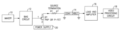
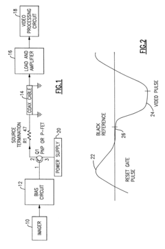
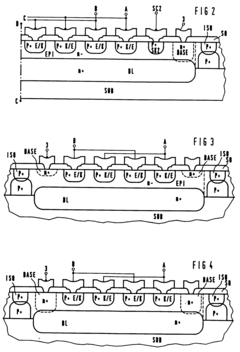
Apparatus using PNP bipolar transistor as buffer to drive video signal
PatentInactiveUS6468201B1
Innovation
- A PNP bipolar transistor or enhancement mode P-channel FET is used as a buffer at the distal end of the endoscope, biased by a base bias circuit and power supply located near the transistor, with the emitter connected through a cable to a load at the proximal end, to drive video signals from the imager to video processing circuits, employing a bias circuit and power supply to maintain signal integrity and reduce power dissipation.
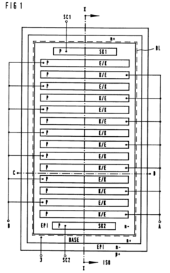
Monolithically integrated PNP transistor structure
PatentInactiveEP0570864A2
Innovation
- A monolithically integrated pnp transistor structure with symmetric emitter and collector regions, interlocking in a comb-like manner, allowing for equal current amplification in both directions with heavily doped regions and optional sense collectors to control saturation, reducing the semiconductor area requirement.
Noise Reduction Techniques in PNP Circuits
Noise reduction techniques in PNP circuits play a crucial role in enhancing signal quality and overall system performance. One of the primary methods involves implementing proper circuit design and layout techniques. By carefully arranging components and minimizing trace lengths, designers can significantly reduce electromagnetic interference (EMI) and radio frequency interference (RFI) that often plague sensitive analog circuits.
Another effective approach is the use of decoupling capacitors strategically placed near the PNP transistor's power supply pins. These capacitors help filter out high-frequency noise and stabilize the voltage supply, ensuring a cleaner signal path. In addition, implementing differential signaling can greatly improve noise immunity by rejecting common-mode noise that affects both signal lines equally.
Shielding is another important technique in noise reduction for PNP circuits. By enclosing sensitive components or entire circuit sections within a conductive enclosure, external electromagnetic interference can be effectively blocked. This is particularly important in applications where the PNP transistor is used for low-level signal amplification or in environments with high electromagnetic noise.
Proper grounding techniques are essential for minimizing noise in PNP circuits. Implementing a star-ground configuration, where all ground connections converge at a single point, can help prevent ground loops and reduce noise coupling between different parts of the circuit. Additionally, using separate analog and digital grounds, with careful consideration of their connection point, can further improve noise performance in mixed-signal designs.
Filtering techniques, such as the implementation of low-pass, high-pass, or band-pass filters, can be employed to attenuate unwanted frequency components in the signal path. These filters can be designed using passive components like resistors and capacitors, or active components including operational amplifiers, to achieve the desired frequency response and noise reduction.
Advanced noise reduction techniques for PNP circuits may also involve the use of chopper stabilization or auto-zeroing techniques. These methods effectively modulate the input signal to shift low-frequency noise and offset voltages to higher frequencies, where they can be more easily filtered out. This approach is particularly useful in precision analog applications where DC accuracy is critical.
In some cases, implementing feedback loops or compensation networks can help reduce noise and improve the overall stability of PNP-based circuits. These techniques can be particularly effective in addressing thermal noise and flicker noise, which are inherent in semiconductor devices.
Thermal Management Strategies for PNP Transistors
Thermal management is a critical aspect of utilizing PNP transistors for advanced signal conditioning. As these devices operate, they generate heat that can significantly impact their performance and reliability. Effective thermal management strategies are essential to maintain optimal operating conditions and extend the lifespan of PNP transistors in signal conditioning applications.
One of the primary thermal management techniques involves proper heat sinking. Heat sinks are designed to dissipate excess heat from the transistor by increasing the surface area available for heat transfer. When selecting a heat sink, factors such as thermal resistance, size, and material composition must be considered. Aluminum and copper are commonly used materials due to their excellent thermal conductivity properties.
In addition to heat sinks, thermal interface materials (TIMs) play a crucial role in enhancing heat transfer between the transistor and the heat sink. These materials, such as thermal greases, pads, or adhesives, fill microscopic air gaps and improve thermal conductivity. The selection of an appropriate TIM depends on factors like thermal conductivity, ease of application, and long-term stability.
Active cooling methods can be employed for more demanding thermal management requirements. Forced-air cooling using fans or blowers can significantly enhance heat dissipation by increasing air circulation around the transistor and heat sink assembly. In extreme cases, liquid cooling systems may be implemented, offering superior heat removal capabilities at the cost of increased complexity and maintenance requirements.
Thermal design considerations should also extend to the printed circuit board (PCB) layout. Proper placement of PNP transistors away from other heat-generating components and the use of thermal vias can help distribute heat more effectively across the board. Copper pour techniques, where large areas of copper are used on the PCB, can also aid in heat spreading and dissipation.
Temperature monitoring and control systems are often integrated into advanced signal conditioning circuits to ensure optimal thermal management. These systems may include temperature sensors, thermal shutdown circuits, and adaptive biasing techniques that adjust transistor operating conditions based on temperature feedback.
Lastly, the selection of appropriate packaging for PNP transistors is crucial for effective thermal management. Packages with low thermal resistance and good heat dissipation properties, such as TO-220 or SOT-223, can significantly improve thermal performance. In some cases, specialized packages with integrated heat spreaders or direct die-attach techniques may be employed for superior thermal management in high-power applications.
Unlock deeper insights with Patsnap Eureka Quick Research — get a full tech report to explore trends and direct your research. Try now!
Generate Your Research Report Instantly with AI Agent
Supercharge your innovation with Patsnap Eureka AI Agent Platform!