Investigating Wastewater Nanofiltration in Semiconductor Production
OCT 15, 202510 MIN READ
Generate Your Research Report Instantly with AI Agent
Patsnap Eureka helps you evaluate technical feasibility & market potential.
Semiconductor Wastewater Nanofiltration Background and Objectives
Nanofiltration technology has emerged as a critical solution for semiconductor manufacturing wastewater treatment over the past three decades. Initially developed in the 1980s as an intermediate filtration technology between reverse osmosis and ultrafiltration, nanofiltration has evolved significantly to address the unique challenges posed by semiconductor production effluents. The semiconductor industry's rapid growth, coupled with increasingly stringent environmental regulations, has accelerated research and development in this specialized application of membrane technology.
The historical trajectory of nanofiltration in semiconductor applications shows a clear progression from simple filtration systems to sophisticated, multi-stage treatment processes. Early implementations focused primarily on removing suspended solids, while modern systems target complex contaminants including heavy metals, organic compounds, and various process chemicals specific to semiconductor fabrication. This evolution has been driven by both technological advancements in membrane materials and the semiconductor industry's transition to more complex manufacturing processes requiring ultrapure water and generating more challenging waste streams.
Current nanofiltration membranes employed in semiconductor wastewater treatment typically operate in the 200-1000 Da molecular weight cut-off range, allowing for selective removal of multivalent ions while permitting some monovalent ions to pass through. This selectivity has proven particularly valuable for recovering valuable materials from semiconductor wastewater, including precious metals and specialized chemicals, while simultaneously reducing environmental impact.
The primary objectives of investigating nanofiltration technology for semiconductor wastewater treatment encompass several interconnected goals. First, to develop more efficient and selective membrane technologies capable of addressing the increasingly complex chemical composition of semiconductor wastewater. Second, to reduce the environmental footprint of semiconductor manufacturing by minimizing discharge volumes and contaminant levels. Third, to enhance resource recovery capabilities, particularly for water reuse within the manufacturing facility and reclamation of valuable materials from waste streams.
Additionally, research aims to address the persistent challenges of membrane fouling and scaling, which remain significant operational concerns in semiconductor applications due to the presence of colloidal silica, metal oxides, and organic compounds in the wastewater. Extending membrane lifespan while maintaining separation efficiency represents a critical technical objective with substantial economic implications for implementation.
The global semiconductor industry's projected growth, with market forecasts exceeding $600 billion by 2025, underscores the urgency of developing advanced wastewater treatment solutions. As chip manufacturing processes continue to advance toward smaller node sizes, the complexity of wastewater streams increases proportionally, creating both technical challenges and opportunities for innovation in nanofiltration technology. This investigation seeks to identify pathways for technological advancement that align with the semiconductor industry's sustainability goals while maintaining economic viability.
Market Demand Analysis for Semiconductor Wastewater Treatment
The semiconductor industry's rapid growth has significantly increased the demand for effective wastewater treatment solutions, particularly nanofiltration technologies. The global semiconductor market, valued at approximately $573 billion in 2022, is projected to reach $1 trillion by 2030, with a corresponding increase in wastewater generation requiring specialized treatment.
Water usage in semiconductor manufacturing is extraordinarily high, with advanced fabrication facilities consuming between 2-4 million gallons daily. This intensive water consumption creates substantial volumes of wastewater containing various contaminants including heavy metals, organic compounds, and chemical residues that require specialized treatment before discharge or recycling.
Environmental regulations worldwide are becoming increasingly stringent regarding semiconductor wastewater discharge. The European Union's Water Framework Directive, China's Water Pollution Prevention and Control Law, and the U.S. Clean Water Act have all established progressively stricter limits on contaminant levels, driving demand for advanced treatment technologies like nanofiltration.
Cost considerations are also driving market demand, as semiconductor manufacturers seek to reduce operational expenses through water recycling. With industrial water costs rising globally at rates of 5-10% annually in many regions, the economic incentive for implementing efficient wastewater treatment and recycling systems has become compelling. Nanofiltration systems, despite their initial capital investment, demonstrate favorable return-on-investment metrics through reduced water procurement costs and discharge fees.
The industry's transition to smaller node sizes (5nm, 3nm, and beyond) has intensified water purity requirements. These advanced manufacturing processes require ultra-pure water and generate wastewater with complex contamination profiles that conventional treatment methods struggle to address effectively, creating specific demand for nanofiltration solutions.
Regional market analysis reveals particularly strong demand growth in Asia-Pacific, where semiconductor manufacturing is concentrated. Taiwan, South Korea, and China collectively account for over 65% of global semiconductor manufacturing capacity, creating concentrated demand for advanced wastewater treatment solutions in these regions.
The sustainability initiatives adopted by major semiconductor manufacturers represent another significant market driver. Companies including TSMC, Samsung, and Intel have established ambitious water conservation targets, with many aiming for 90-100% water recycling rates by 2030, directly increasing demand for advanced filtration technologies.
Market forecasts indicate the semiconductor wastewater treatment sector will grow at a CAGR of 6.8% through 2028, with nanofiltration technologies expected to outpace this growth rate due to their superior performance characteristics and ability to address emerging contaminants of concern.
Current Nanofiltration Technologies and Implementation Challenges
Nanofiltration (NF) technology has emerged as a critical solution for wastewater treatment in semiconductor manufacturing, positioned between reverse osmosis and ultrafiltration in terms of selectivity and operating pressure. Current commercial NF membranes primarily utilize thin-film composite structures consisting of a thin polyamide selective layer (typically 50-200 nm) on top of a porous support. These membranes effectively remove multivalent ions, organic compounds, and particles larger than 1 nm while allowing some monovalent ions to pass through.
The semiconductor industry predominantly employs spiral-wound and hollow fiber NF membrane configurations. Spiral-wound modules offer high packing density and moderate fouling resistance, while hollow fiber modules provide higher surface area-to-volume ratios but are more susceptible to fouling. Recent advancements have introduced ceramic nanofiltration membranes with superior chemical and thermal stability, particularly valuable for treating aggressive semiconductor wastewater containing strong acids, bases, and solvents.
Automated membrane cleaning systems represent another significant technological advancement, utilizing combinations of chemical cleaning agents and physical methods to maintain membrane performance. These systems can be programmed to initiate cleaning cycles based on pressure differential triggers or predetermined schedules, minimizing downtime and extending membrane life.
Despite these advancements, several implementation challenges persist in semiconductor wastewater nanofiltration. Membrane fouling remains the most significant operational challenge, with inorganic scaling, organic fouling, and biofouling all contributing to performance decline. The complex and variable composition of semiconductor wastewater, containing metals, organic solvents, and various chemicals, accelerates fouling rates and complicates cleaning protocols.
Energy consumption presents another substantial challenge, with nanofiltration systems requiring significant pumping energy to maintain the necessary transmembrane pressure (typically 5-20 bar). This energy requirement impacts operational costs and environmental footprint, though less severe than reverse osmosis systems.
Selective removal capabilities also present technical limitations, as current NF membranes struggle to achieve consistent separation performance across the diverse contaminant profile in semiconductor wastewater. Certain compounds like boron and some low-molecular-weight organics prove particularly difficult to remove efficiently.
Integration challenges with existing treatment systems further complicate implementation, as nanofiltration must function effectively within broader wastewater treatment trains. Compatibility issues with upstream and downstream processes, space constraints in existing facilities, and the need for specialized pre-treatment to protect membranes all present significant engineering challenges that must be addressed for successful deployment.
Existing Nanofiltration Solutions for Semiconductor Wastewater
01 Nanofiltration membrane materials and structures
Various materials and structures are used in nanofiltration membranes for wastewater treatment. These include composite membranes with specialized layers, modified polymeric materials, and novel nanostructured materials that enhance filtration efficiency. The membrane structure can be optimized for specific contaminant removal while maintaining high flux rates and minimizing fouling. Advanced manufacturing techniques allow for precise control of pore size and surface properties.- Nanofiltration membrane materials and structures: Various materials and structures are used in nanofiltration membranes for wastewater treatment. These include composite membranes with specialized layers, modified polymeric materials, and novel nanostructured materials that enhance filtration efficiency. The membrane structure can be optimized for specific contaminant removal while maintaining high flux rates and reducing fouling tendencies.
- Integrated wastewater treatment systems with nanofiltration: Nanofiltration is often integrated into comprehensive wastewater treatment systems. These systems combine multiple treatment stages including pre-treatment, nanofiltration, and post-treatment processes to achieve optimal water purification. The integration enhances overall system efficiency, reduces energy consumption, and enables the treatment of complex wastewater streams with varying contaminant profiles.
- Industrial wastewater treatment applications: Nanofiltration technology is applied to treat various industrial wastewaters containing heavy metals, organic pollutants, and other contaminants. Specialized nanofiltration processes are designed for specific industries such as textile, pharmaceutical, mining, and chemical manufacturing. These applications focus on contaminant removal efficiency, water recovery rates, and the potential for resource recovery from wastewater streams.
- Anti-fouling and membrane cleaning technologies: Membrane fouling is a significant challenge in nanofiltration systems. Various anti-fouling strategies have been developed, including surface modifications, operational parameter optimization, and novel cleaning protocols. These technologies extend membrane life, maintain filtration efficiency, and reduce operational costs by minimizing the frequency of membrane replacement and system downtime.
- Energy-efficient nanofiltration processes: Energy efficiency is crucial for sustainable wastewater treatment. Advanced nanofiltration processes incorporate energy recovery systems, optimized operating pressures, and improved flow dynamics to reduce energy consumption. These innovations include pressure-assisted osmosis, hybrid energy systems, and smart control mechanisms that adjust operational parameters based on feed water quality and desired output specifications.
02 Integrated wastewater treatment systems using nanofiltration
Nanofiltration is often integrated into comprehensive wastewater treatment systems. These systems combine nanofiltration with other treatment processes such as pre-filtration, biological treatment, or advanced oxidation to achieve optimal results. The integration allows for targeted removal of specific contaminants while optimizing energy consumption and operational efficiency. Such systems can be designed for various scales from industrial applications to municipal treatment facilities.Expand Specific Solutions03 Industrial wastewater treatment applications
Nanofiltration technology is specifically adapted for various industrial wastewater streams with unique contaminant profiles. Applications include treatment of textile effluents, pharmaceutical waste, mining wastewater, and food processing wastewater. The nanofiltration processes are customized based on the specific contaminants present, concentration levels, and desired water quality outcomes. These specialized applications often require modified membrane properties or operating conditions to handle challenging industrial pollutants.Expand Specific Solutions04 Fouling prevention and membrane cleaning techniques
Membrane fouling is a significant challenge in nanofiltration systems. Various techniques have been developed to prevent fouling and extend membrane life, including surface modifications, anti-fouling coatings, and optimized operational parameters. Cleaning protocols using chemical, physical, or combined approaches help restore membrane performance. Advanced monitoring systems can detect early signs of fouling and trigger automated cleaning sequences to maintain system efficiency.Expand Specific Solutions05 Resource recovery from wastewater using nanofiltration
Nanofiltration enables the recovery of valuable resources from wastewater streams. This includes the selective separation and concentration of nutrients, metals, and other valuable compounds that can be reused or sold. The technology allows for the creation of closed-loop systems where water is recycled and valuable components are extracted. This approach transforms wastewater treatment from a purely environmental necessity into a potential revenue-generating process through resource recovery.Expand Specific Solutions
Leading Companies and Research Institutions in Nanofiltration
The nanofiltration wastewater treatment market in semiconductor production is in a growth phase, driven by increasing environmental regulations and water scarcity concerns. The market is expected to expand significantly as semiconductor manufacturing capacity grows globally. Technology maturity varies across players, with established companies like Taiwan Semiconductor Manufacturing Co. (TSMC), Samsung Electronics, and GLOBALFOUNDRIES leading innovation in advanced filtration systems. Asian companies, particularly from Taiwan, South Korea, and Japan (including Kurita Water Industries and Nomura Micro Science), dominate the landscape with specialized expertise. Western players like Siemens and Lam Research contribute complementary technologies. The Industrial Technology Research Institute serves as a key R&D hub, while Chinese firms like SMIC are rapidly advancing their capabilities to meet domestic semiconductor expansion needs.
Taiwan Semiconductor Manufacturing Co., Ltd.
Technical Solution: TSMC has pioneered an integrated nanofiltration system for semiconductor wastewater treatment that focuses on maximizing water reuse while meeting ultra-pure water requirements. Their approach utilizes specialized cross-linked aromatic polyamide thin-film composite membranes with controlled surface charge characteristics to selectively remove contaminants common in semiconductor manufacturing, including metal ions, photoresist residues, and chemical mechanical planarization (CMP) waste. The system operates in a multi-stage configuration with pH adjustment capabilities to optimize removal efficiency for different contaminant profiles. TSMC's nanofiltration technology achieves over 98% removal of critical contaminants while maintaining flow rates of 20-30 LMH (liters per square meter per hour). Their water recycling systems incorporating this technology have enabled water reuse rates exceeding 85% in their fabrication facilities, significantly reducing freshwater consumption. The company has also developed proprietary anti-fouling coatings and cleaning protocols that extend membrane life by up to 30% compared to industry standards.
Strengths: Highly optimized for semiconductor-specific contaminants with exceptional removal efficiency and integration with existing fab water systems. Demonstrates proven performance at industrial scale with significant water conservation results. Weaknesses: Requires substantial technical expertise to operate and maintain, and the specialized membrane materials increase replacement costs compared to standard filtration options.
Kurita Water Industries Ltd.
Technical Solution: Kurita has developed advanced nanofiltration (NF) membrane systems specifically designed for semiconductor wastewater treatment. Their technology employs composite polyamide thin-film membranes with optimized pore sizes (typically 1-5 nm) to effectively remove dissolved solids, organic compounds, and metal ions while allowing water molecules to pass through. The system operates at lower pressures (5-15 bar) compared to reverse osmosis, reducing energy consumption by approximately 30%. Kurita's integrated approach combines nanofiltration with pre-treatment processes including coagulation and ultrafiltration to prevent membrane fouling and extend operational lifetime. Their systems achieve recovery rates of 85-90% and can remove over 95% of multivalent ions and 60-80% of monovalent ions from semiconductor wastewater. The company has implemented real-time monitoring systems with automated cleaning cycles to maintain consistent performance in high-purity water applications.
Strengths: Superior removal efficiency for semiconductor-specific contaminants while maintaining lower energy consumption compared to reverse osmosis. Comprehensive integration with other treatment technologies creates a holistic solution. Weaknesses: Higher initial capital investment compared to conventional filtration systems, and potential for membrane fouling when treating wastewater with high organic content or silica compounds.
Key Patents and Technical Innovations in Nanofiltration Membranes
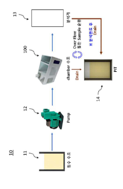
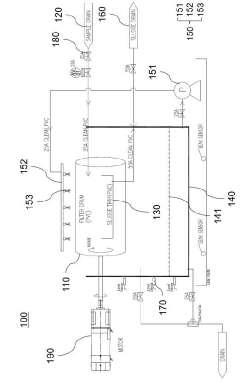
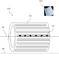
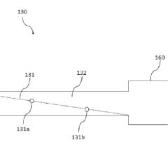
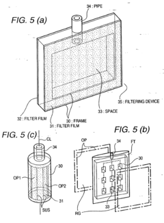
A sample water filtration device that provides sample water filtered from semiconductor production process wastewater to the analyzer
PatentPendingKR1020240014967A
Innovation
- A miniaturized sample water filtration device with a mesh drum and cleaning unit that rotates to separate sludge, allowing for automatic cleaning and extended filter replacement cycles, ensuring continuous analysis by removing impurities.
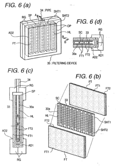
Method of fabricating a semiconductor device with process liquid recycling
PatentInactiveEP1055446B1
Innovation
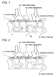
- A filtering method utilizing filters made from removables that form smaller pores over time, allowing for the recirculation of wastewater to enhance filtration efficiency and reduce costs by forming a second filter with smaller pores on the first filter surface, which can trap smaller particles and maintain filtering performance through external forces.
Environmental Compliance and Sustainability Considerations
The semiconductor industry faces increasingly stringent environmental regulations worldwide, necessitating comprehensive compliance strategies for wastewater management. Current regulatory frameworks include the Clean Water Act in the United States, the Water Framework Directive in the European Union, and similar legislation in Asian manufacturing hubs like Taiwan, South Korea, and Japan. These regulations establish strict discharge limits for heavy metals, organic compounds, and other contaminants commonly found in semiconductor wastewater.
Nanofiltration technology offers semiconductor manufacturers a viable pathway to meet and exceed these regulatory requirements. By implementing advanced nanofiltration systems, facilities can significantly reduce their environmental footprint while simultaneously addressing compliance challenges. The technology's ability to remove specific contaminants at the molecular level aligns perfectly with the precision requirements of environmental regulations targeting the semiconductor industry.
Beyond mere compliance, nanofiltration supports broader sustainability initiatives within semiconductor manufacturing. Water scarcity represents a critical challenge for the industry, which traditionally consumes vast quantities of ultrapure water. Nanofiltration enables effective water recycling and reuse, potentially reducing freshwater consumption by 30-60% depending on implementation specifics. This conservation aspect becomes increasingly valuable as manufacturing expands in water-stressed regions globally.
Energy efficiency considerations also factor prominently in sustainability assessments of nanofiltration systems. While nanofiltration requires less energy than reverse osmosis, optimization remains crucial for minimizing the carbon footprint of wastewater treatment operations. Recent innovations in membrane materials and system design have yielded energy efficiency improvements of approximately 15-25% compared to earlier generation systems.
Chemical usage reduction represents another significant sustainability benefit of nanofiltration implementation. Traditional wastewater treatment often relies heavily on chemical additives for precipitation and flocculation processes. Nanofiltration's physical separation mechanism substantially reduces chemical requirements, decreasing both environmental impact and operational costs. Studies indicate chemical consumption reductions of 40-70% are achievable when nanofiltration replaces conventional treatment methods.
Life cycle assessment (LCA) methodologies increasingly inform sustainability evaluations of wastewater treatment technologies in semiconductor manufacturing. Comprehensive LCAs examining nanofiltration implementations reveal favorable environmental profiles when considering factors such as embodied energy, carbon emissions, and resource consumption across the entire system lifecycle. These assessments typically demonstrate that the environmental benefits of water recovery and contaminant removal outweigh the impacts associated with membrane production and system operation.
Economic Feasibility and Return on Investment Analysis
The implementation of nanofiltration systems for wastewater treatment in semiconductor manufacturing requires substantial initial investment, yet offers compelling long-term economic benefits. Initial capital expenditures typically range from $2-5 million for medium-scale facilities, encompassing membrane systems, pumping equipment, monitoring technology, and integration with existing treatment infrastructure. These costs vary significantly based on production volume, wastewater characteristics, and desired recovery rates.
Operational expenses include membrane replacement (occurring every 2-4 years), energy consumption (approximately 1-3 kWh per cubic meter of treated water), chemical cleaning agents, and specialized maintenance personnel. However, these costs are offset by several revenue streams and cost-saving mechanisms that enhance the economic viability of nanofiltration implementation.
The most significant economic benefit derives from water recycling capabilities, with advanced nanofiltration systems achieving 70-85% water recovery rates. For a facility processing 1,000 cubic meters daily, this translates to annual savings of $500,000-750,000 in water procurement costs alone. Additionally, the recovery of valuable materials such as copper, gold, and rare earth elements from wastewater streams can generate secondary revenue of $100,000-300,000 annually depending on production type.
Return on investment analysis indicates payback periods ranging from 2.5-4 years for most semiconductor facilities. Sensitivity analysis reveals that facilities in water-scarce regions or those facing stringent discharge regulations experience accelerated ROI timelines, sometimes achieving breakeven in under 2 years. Conversely, smaller operations with lower wastewater volumes may experience extended payback periods of 5-7 years without additional incentives.
Risk assessment identifies several factors affecting economic performance, including membrane fouling rates, energy price fluctuations, and regulatory changes. Monte Carlo simulations suggest that despite these variables, 85% of implementation scenarios achieve positive net present value within a 5-year horizon, with internal rates of return averaging 18-25%.
Government incentives significantly enhance economic feasibility, with tax credits, grants, and accelerated depreciation schedules available in many jurisdictions. These incentives can reduce initial capital requirements by 15-30% and improve ROI metrics accordingly. Furthermore, carbon credit opportunities are emerging as water treatment efficiency increasingly factors into emissions calculations, potentially adding $50,000-100,000 in annual value through carbon market participation.
Unlock deeper insights with Patsnap Eureka Quick Research — get a full tech report to explore trends and direct your research. Try now!
Generate Your Research Report Instantly with AI Agent
Supercharge your innovation with Patsnap Eureka AI Agent Platform!