Laser Patterning Techniques For High Resolution Liquid Metal Lines
AUG 28, 202510 MIN READ
Generate Your Research Report Instantly with AI Agent
PatSnap Eureka helps you evaluate technical feasibility & market potential.
Laser Patterning Technology Background and Objectives
Laser patterning technology has evolved significantly over the past three decades, transitioning from basic material ablation techniques to sophisticated high-precision manufacturing processes. Initially developed for semiconductor fabrication in the 1980s, laser patterning has expanded into diverse applications including printed electronics, microfluidics, and most recently, liquid metal patterning. The fundamental principle involves using focused laser energy to selectively modify material properties or remove material with exceptional spatial control.
The evolution of laser sources has been pivotal in this technological progression. Early systems primarily utilized CO2 and Nd:YAG lasers, while contemporary applications leverage ultrafast femtosecond lasers, fiber lasers, and excimer lasers that offer unprecedented precision down to nanometer scales. This advancement has enabled the creation of increasingly fine features with minimal thermal damage to surrounding materials.
For liquid metal patterning specifically, the technology has emerged as a promising solution to address the growing demand for flexible, stretchable, and reconfigurable electronics. Liquid metals, particularly gallium-based alloys like eutectic gallium-indium (EGaIn), possess unique properties including high electrical conductivity, excellent thermal conductivity, and inherent fluidity that make them ideal candidates for next-generation electronic applications.
The primary technical objective in laser patterning of liquid metals is achieving high-resolution conductive lines (sub-10 μm) while maintaining electrical performance and mechanical stability. This presents unique challenges compared to traditional solid metal patterning due to the fluid nature of the materials, their surface tension characteristics, and oxidation behaviors. Current research aims to optimize laser parameters including wavelength, pulse duration, energy density, and scanning strategies to precisely control the liquid metal deposition and patterning process.
Secondary objectives include developing techniques for multi-layer patterning, improving adhesion to various substrate materials, and enhancing the long-term stability of patterned liquid metal structures. The field is also exploring hybrid approaches that combine laser patterning with complementary techniques such as inkjet printing or microfluidic delivery systems to overcome current limitations.
The trajectory of this technology points toward enabling a new generation of electronic devices including soft robotics, wearable health monitors, and reconfigurable antennas. As manufacturing processes continue to mature, the integration of high-resolution liquid metal patterning into commercial production environments represents a significant opportunity for innovation in flexible electronics manufacturing.
Market Applications for High-Resolution Liquid Metal Lines
The integration of high-resolution liquid metal lines enabled by laser patterning techniques is creating significant market opportunities across multiple industries. The electronics sector represents the primary application domain, with flexible and stretchable electronics emerging as a rapidly growing segment. These technologies enable the development of wearable health monitors, smart textiles, and bendable displays that conform to non-planar surfaces while maintaining electrical functionality. Market analysts project the flexible electronics sector to expand at a compound annual growth rate exceeding 15% through 2030, driven by consumer demand for unobtrusive, comfortable wearable devices.
Medical device manufacturing constitutes another promising application area, where high-resolution liquid metal patterns facilitate the creation of biocompatible sensors and electrodes for neural interfaces, cardiac monitoring systems, and minimally invasive surgical tools. The precision offered by laser patterning techniques allows for intricate circuit designs that can interface directly with biological tissues while maintaining signal integrity in challenging physiological environments.
Aerospace and defense applications represent a high-value market segment, with liquid metal lines enabling conformal antennas, radar systems, and electromagnetic shielding solutions that can be integrated directly onto curved structural components. The ability to create high-resolution conductive patterns on three-dimensional surfaces addresses longstanding challenges in aircraft and satellite design, where space constraints and aerodynamic considerations limit traditional circuit implementation approaches.
The automotive industry is increasingly adopting advanced electronics for autonomous driving systems, requiring sensors and processing units that can withstand vibration, temperature fluctuations, and mechanical stress. High-resolution liquid metal lines offer superior durability compared to conventional rigid circuit boards, creating opportunities for more reliable vehicle electronics and embedded sensing networks throughout automotive structures.
Energy harvesting and storage systems benefit from liquid metal patterning through improved interconnects for solar cells, flexible batteries, and supercapacitors. The enhanced conductivity and mechanical resilience of laser-patterned liquid metal lines contribute to higher efficiency energy conversion and storage solutions, particularly for applications requiring conformability to irregular surfaces.
Emerging applications in soft robotics leverage the unique properties of liquid metal lines to create adaptive sensing skins and reconfigurable actuator networks. These technologies enable robots with unprecedented dexterity and environmental awareness, opening new markets in industrial automation, healthcare assistance, and consumer robotics.
The Internet of Things (IoT) ecosystem represents perhaps the broadest application domain, with high-resolution liquid metal lines enabling seamless integration of sensing, computing, and communication capabilities into everyday objects and environments. As IoT deployments accelerate across industrial, commercial, and residential settings, the demand for reliable, unobtrusive electronic components continues to grow, creating sustained market opportunities for advanced manufacturing techniques like laser patterning of liquid metals.
Current Challenges in Liquid Metal Patterning Techniques
Despite significant advancements in liquid metal patterning techniques, several critical challenges persist that limit the widespread application of high-resolution liquid metal lines created through laser patterning. The primary obstacle remains the inherent surface tension of liquid metals, particularly gallium-based alloys like EGaIn and Galinstan. This high surface tension (approximately 624 mN/m for gallium at room temperature) causes the metal to form spherical droplets rather than maintaining desired linear patterns, significantly hampering the achievement of fine feature sizes below 10 μm.
Oxide skin formation presents another substantial challenge. While the spontaneous formation of a thin oxide layer on liquid metal surfaces provides some stability to patterns, controlling this oxidation process with precision during laser patterning remains difficult. The oxide layer's thickness and properties can vary unpredictably based on environmental conditions, affecting pattern resolution and electrical performance.
Substrate compatibility issues further complicate the patterning process. Many substrates exhibit poor wettability with liquid metals, necessitating surface modifications or adhesion layers that add complexity to the fabrication process. Additionally, thermal management during laser patterning is critical, as excessive heat can cause substrate damage or undesired changes in the liquid metal properties, while insufficient energy may result in incomplete pattern formation.
The viscosity characteristics of liquid metals present a paradoxical challenge: while their fluidity enables self-healing properties beneficial for flexible electronics, it simultaneously makes maintaining precise pattern geometries difficult, especially when subjected to mechanical deformation. This becomes particularly problematic in applications requiring stable, high-resolution features under dynamic conditions.
Scalability and reproducibility remain significant hurdles for industrial implementation. Current laboratory techniques often demonstrate impressive results but struggle with consistency across larger areas or in high-volume production scenarios. The parameter space for laser patterning (including power, scan speed, focus, and pulse characteristics) is extensive and highly interdependent, making process optimization challenging.
Integration challenges with conventional electronics manufacturing processes also persist. Liquid metal patterning techniques often require specialized handling and processing steps that are not readily compatible with established semiconductor fabrication methods, creating barriers to adoption in mainstream electronics manufacturing.
Finally, long-term stability of patterned liquid metal structures remains a concern. Environmental factors such as humidity, temperature fluctuations, and oxidation over time can alter the electrical and mechanical properties of liquid metal patterns, potentially affecting device reliability and performance longevity.
State-of-the-Art Laser Patterning Solutions for Liquid Metals
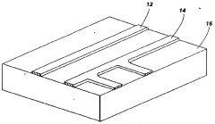
01 Direct laser patterning of liquid metal lines
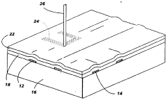
Direct laser patterning techniques can be used to create precise liquid metal lines with high resolution. This approach involves using focused laser beams to selectively pattern liquid metal on various substrates. The laser energy can be controlled to achieve different line widths and resolutions, making it suitable for creating intricate circuit patterns. This technique offers advantages in terms of speed, precision, and the ability to work with various liquid metal compositions.- Direct laser patterning of liquid metal lines: Direct laser patterning techniques can be used to create precise liquid metal lines with high resolution. This approach involves using focused laser beams to selectively pattern liquid metal materials on various substrates. The laser energy causes localized heating that enables the liquid metal to adhere to specific areas while maintaining defined edges. This technique allows for fine control over line width and pattern complexity, making it suitable for high-resolution electronic circuits and interconnects.
- Laser sintering of metal nanoparticle inks: Laser sintering techniques can be applied to metal nanoparticle inks to create liquid metal lines with precise resolution. This process involves depositing metal nanoparticle inks onto a substrate and then using laser energy to sinter the particles together, forming continuous conductive pathways. The sintering process transforms the discrete nanoparticles into cohesive liquid metal lines with well-defined boundaries. This approach enables the creation of fine features and can be performed at relatively low temperatures, making it compatible with various substrate materials.
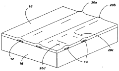
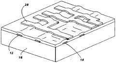
- Laser ablation for liquid metal patterning: Laser ablation techniques can be employed to pattern liquid metal lines with high resolution. This subtractive approach involves using laser energy to selectively remove material from a continuous liquid metal film, leaving behind the desired pattern. The precision of the laser beam allows for the creation of intricate designs with sharp edges and fine features. By controlling laser parameters such as power, pulse duration, and spot size, the resolution of the liquid metal lines can be optimized for specific applications in flexible electronics and microfluidic devices.
- Laser-assisted transfer printing of liquid metals: Laser-assisted transfer printing techniques enable the precise deposition of liquid metal lines with controlled resolution. This approach uses laser energy to transfer liquid metal from a donor substrate to a receiver substrate in a defined pattern. The laser pulse provides the energy needed to propel the liquid metal across the gap between substrates while maintaining pattern fidelity. This non-contact printing method allows for high-resolution patterning on various substrate materials, including flexible and temperature-sensitive substrates, making it valuable for next-generation electronic devices.
- Hybrid laser techniques for multi-resolution liquid metal patterning: Hybrid laser techniques combine multiple laser-based approaches to achieve optimal resolution for liquid metal lines across different feature sizes. These methods may integrate direct writing, sintering, and ablation in a single process flow to leverage the advantages of each technique. For example, coarse features might be created using direct laser writing, while fine details are added through precise laser ablation. This hybrid approach enables the fabrication of complex circuits with varying line widths and resolutions, offering versatility for advanced electronic applications requiring both large conductive traces and fine interconnects.
02 Laser-assisted deposition and sintering of metal particles
This technique involves the laser-assisted deposition and sintering of metal particles to form conductive lines. Metal nanoparticles or microparticles are deposited onto a substrate and then selectively sintered using laser energy to create conductive pathways. The resolution of the lines depends on the laser spot size, energy density, and the properties of the metal particles. This approach allows for the creation of fine metal lines with controlled electrical properties and good adhesion to the substrate.Expand Specific Solutions03 Photolithographic techniques combined with laser processing
Combining photolithographic techniques with laser processing can enhance the resolution of liquid metal lines. This hybrid approach involves creating patterns using photolithography followed by laser processing to define or refine the liquid metal lines. The photoresist patterns serve as templates or masks for the subsequent laser processing steps. This combination allows for achieving higher resolution and more complex patterns than would be possible with either technique alone.Expand Specific Solutions04 Laser ablation for patterning liquid metal films
Laser ablation can be used to pattern pre-deposited liquid metal films to create high-resolution lines. In this technique, a continuous film of liquid metal is first deposited on a substrate, and then a laser beam selectively removes unwanted portions to create the desired pattern. The resolution of the lines depends on the laser parameters such as wavelength, pulse duration, and energy density. This subtractive approach offers advantages in terms of precision and the ability to create complex patterns with minimal material waste.Expand Specific Solutions05 Advanced laser techniques for ultra-fine resolution
Advanced laser techniques such as femtosecond laser processing and two-photon polymerization can be used to achieve ultra-fine resolution in liquid metal patterning. These techniques utilize ultra-short laser pulses or non-linear optical effects to achieve feature sizes below the diffraction limit. By precisely controlling the laser parameters and utilizing specialized optical setups, it is possible to create liquid metal lines with resolutions in the sub-micron range, which is essential for advanced microelectronic applications.Expand Specific Solutions
Leading Companies and Research Institutions in Laser Patterning
Laser patterning techniques for high-resolution liquid metal lines are currently in an emerging growth phase, with the market expanding rapidly due to increasing applications in flexible electronics and printed circuit technologies. The global market is estimated to reach $3.5 billion by 2025, driven by demand for miniaturized electronic components. Technologically, the field is advancing from experimental to commercial maturity, with key players demonstrating varying levels of expertise. Samsung Electronics and FUJIFILM lead with advanced R&D capabilities, while academic institutions like Huazhong University and Shenzhen University contribute fundamental research breakthroughs. Companies including DuPont, Motorola Solutions, and Seiko Epson are developing specialized applications, while materials specialists such as DIC Corp and InkTec focus on compatible conductive inks and substrates for these high-precision patterning techniques.
Samsung Electronics Co., Ltd.
Technical Solution: Samsung has developed advanced laser patterning techniques for high-resolution liquid metal lines that integrate seamlessly with their flexible display and semiconductor manufacturing processes. Their approach utilizes femtosecond laser direct writing combined with selective wetting surface modification to achieve line widths below 10 μm. The process involves a two-step method where the laser first creates hydrophilic/hydrophobic patterns on substrate surfaces, followed by selective deposition of liquid metal alloys (primarily gallium-based) that adhere only to the laser-treated areas. Samsung has implemented this technology in their flexible electronics division, achieving conductivity values approaching 3.4 × 10^6 S/m while maintaining flexibility under mechanical deformation. Their manufacturing system incorporates real-time optical monitoring to ensure pattern fidelity and employs proprietary surface chemistry treatments to enhance metal adhesion while preventing oxidation.
Strengths: Exceptional resolution capability (sub-10 μm) with high conductivity retention during bending cycles; seamless integration with existing semiconductor manufacturing infrastructure; excellent scalability for mass production. Weaknesses: Requires precise environmental control during patterning; higher initial equipment investment compared to conventional methods; limited compatibility with certain substrate materials.
Seiko Epson Corp.
Technical Solution: Seiko Epson has developed a comprehensive laser patterning technology for high-resolution liquid metal lines that builds upon their extensive expertise in precision printing and microfabrication. Their approach combines digital laser processing with microfluidic delivery systems to achieve line widths down to 8 μm with exceptional uniformity. The process begins with application of a proprietary surface modification layer that creates regions with controlled wettability. A diode-pumped solid-state laser (532 nm) then selectively modifies this layer to create hydrophilic pathways with precise geometry. Epson's custom-formulated liquid metal alloy—primarily gallium-based with proprietary additives to control oxidation and surface tension—is then delivered through a piezoelectric micropump system that precisely controls volume and flow rate. The company has integrated this technology with their existing manufacturing infrastructure, enabling high-throughput production on both rigid and flexible substrates. Epson has successfully implemented this technology in their advanced display components and flexible circuit applications, achieving conductivity values of approximately 3.0 × 10^6 S/m while maintaining mechanical flexibility through over 10,000 bending cycles. Their system incorporates in-line quality monitoring using optical and electrical characterization to ensure consistent performance.
Strengths: Excellent integration with existing manufacturing systems; superior line uniformity and edge definition; highly scalable process suitable for mass production environments. Weaknesses: Requires specialized liquid metal handling infrastructure; more sensitive to substrate surface quality variations than some competing technologies; higher implementation costs for smaller production runs.
Key Patents and Technical Breakthroughs in Laser Microfabrication
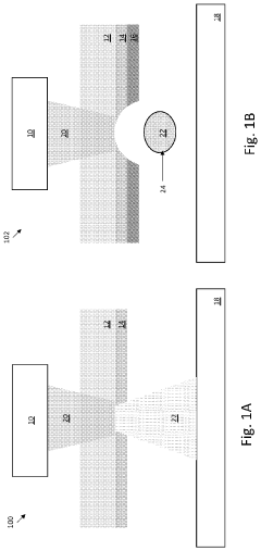
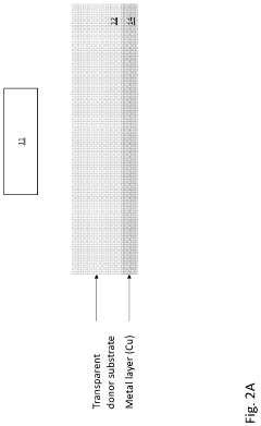
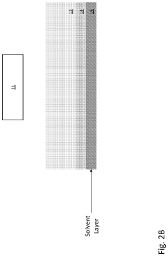
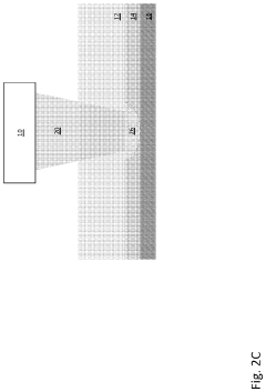
Systems and methods for printing metal lines and patterns at high resolution
PatentActiveUS20230398802A1
Innovation
- A method involving a metal-coated transparent donor substrate with a solvent layer, where a laser heats the metal to eject nano particles constrained within a solvent membrane, allowing precise deposition of metal lines with high resolution and conductivity equivalent to pure metal by controlling the trajectory and evaporating the solvent to form conductive patterns.
High resolution conductor patterning
PatentInactiveUS4942110A
Innovation
- A method involving the application of a uniformly coated thick film material to a substrate, followed by oven-drying and pattern generation using a focused laser beam to harden the material, allowing for high-resolution patterning on uneven surfaces by scanning the laser across the substrate or moving the substrate under computer control, with unexposed material easily removable and the pattern fired to ensure operational characteristics.
Materials Compatibility and Processing Parameters
The compatibility between liquid metals and substrate materials represents a critical factor in laser patterning techniques for high-resolution liquid metal lines. Gallium-based liquid metals, particularly eutectic gallium-indium (EGaIn) and gallium-indium-tin (Galinstan), demonstrate varying adhesion properties depending on substrate composition. Polymeric substrates such as polydimethylsiloxane (PDMS), polyethylene terephthalate (PET), and polyimide exhibit different wettability characteristics, with oxygen plasma treatment significantly enhancing adhesion through surface energy modification.
Processing parameters for laser patterning must be precisely calibrated to achieve optimal resolution without damaging either the liquid metal or substrate. Laser power density typically ranges from 0.5-5 W/cm² for thin-film applications, with higher densities risking thermal damage to polymeric substrates. Pulse duration represents another critical parameter, with ultrashort pulses (femtosecond to picosecond range) minimizing heat-affected zones and enabling finer feature resolution compared to nanosecond or continuous wave lasers.
Scan speed directly impacts line resolution, with optimal values between 10-100 mm/s depending on substrate thermal properties. Slower speeds increase energy deposition, potentially causing excessive oxidation of liquid metals, while faster speeds may result in discontinuous patterns. The focal spot size, typically adjusted between 10-50 μm, determines the theoretical minimum line width achievable, though practical resolution is often 1.2-1.5 times larger due to thermal diffusion effects.
Environmental conditions during processing significantly influence pattern quality. Controlled atmosphere chambers using inert gases like argon or nitrogen prevent unwanted oxidation of liquid metals during patterning. Humidity levels below 40% are generally recommended to minimize oxide formation that could impede electrical conductivity. Temperature control within ±2°C during processing ensures consistent viscosity and surface tension properties of liquid metals.
Pre-treatment and post-processing steps further enhance pattern quality and stability. Substrate cleaning protocols using isopropyl alcohol or acetone followed by oxygen plasma treatment (30-60 seconds at 50-100W) optimize surface energy for liquid metal adhesion. Post-patterning treatments including selective passivation using thin fluoropolymer coatings or silane compounds can prevent oxidation while maintaining electrical functionality of the patterned lines.
Multi-layer processing considerations become essential for complex device fabrication, requiring precise alignment systems with accuracy better than ±5 μm between successive patterning steps. Thermal management strategies including substrate cooling or multi-pass processing with reduced energy per pass help maintain dimensional stability when creating high-density interconnect patterns.
Environmental and Safety Considerations in Laser Processing
Laser patterning of liquid metal lines, while offering significant technological advantages, presents several environmental and safety considerations that must be addressed in industrial applications. The laser processing of liquid metals, particularly gallium-based alloys commonly used in flexible electronics, involves potential hazards related to material toxicity, laser operation, and waste management. Gallium and its alloys, though less toxic than mercury, still require proper handling protocols to prevent workplace exposure through inhalation or skin contact, which can cause irritation and potential long-term health effects.
The laser systems employed in high-resolution patterning generate significant optical hazards. Class 4 lasers, often used in industrial applications, can cause severe eye damage and skin burns without proper protective measures. Facilities must implement comprehensive safety protocols including appropriate eyewear, enclosed beam paths, and restricted access to laser operation areas. Additionally, the interaction between high-power lasers and target materials can produce harmful fumes, particulates, and aerosols, necessitating adequate ventilation systems with appropriate filtration capabilities.
Thermal management represents another critical safety consideration. The localized heating during laser patterning can create fire hazards, particularly when processing liquid metals in the presence of oxidizing agents or flammable materials. Temperature monitoring systems and fire suppression equipment must be integrated into processing environments to mitigate these risks. Furthermore, electrical safety measures are essential when working with conductive liquid metals near laser equipment with high-voltage components.
From an environmental perspective, waste management of processed liquid metals requires careful consideration. Gallium-based alloys and their oxides must be properly collected and disposed of according to relevant regulations to prevent environmental contamination. The energy consumption of laser systems also presents environmental concerns, with high-power lasers demanding significant electricity. Implementation of energy-efficient laser sources and optimized processing parameters can reduce the carbon footprint of these manufacturing processes.
Regulatory compliance represents a final critical consideration. Manufacturers employing laser patterning for liquid metal lines must adhere to various standards including OSHA regulations, ANSI Z136 laser safety standards, and environmental protection guidelines. Regular safety audits, employee training programs, and documentation of safety protocols are essential components of a comprehensive safety management system for laser processing facilities working with liquid metals.
Unlock deeper insights with PatSnap Eureka Quick Research — get a full tech report to explore trends and direct your research. Try now!
Generate Your Research Report Instantly with AI Agent
Supercharge your innovation with PatSnap Eureka AI Agent Platform!