Material Jetting Electronics Enclosures: ESD Behavior, Shielding And Flammability
SEP 12, 20259 MIN READ
Generate Your Research Report Instantly with AI Agent
Patsnap Eureka helps you evaluate technical feasibility & market potential.
Material Jetting Technology Background and Objectives
Material Jetting (MJ) represents a significant advancement in additive manufacturing technologies, emerging in the late 1990s and gaining substantial traction in the 2010s. This technology operates on the principle of selectively depositing droplets of build materials onto a build platform, similar to traditional inkjet printing but in three dimensions. The materials, typically photopolymers or waxes, are then cured or solidified using ultraviolet light or other curing mechanisms to create precise, high-resolution parts.
The evolution of Material Jetting has been marked by continuous improvements in material properties, process control, and application versatility. Initially limited to prototype visualization, the technology has progressively expanded to functional prototyping and, more recently, to end-use part production. This progression has been driven by advancements in material science, particularly the development of multi-material capabilities and materials with enhanced mechanical, thermal, and electrical properties.
In the context of electronics enclosures, Material Jetting offers unique advantages including high dimensional accuracy, smooth surface finish, and the ability to produce complex geometries with internal features. These characteristics make it particularly suitable for creating housings for sensitive electronic components where precision and customization are paramount.
The primary technical objective in applying Material Jetting to electronics enclosures is to address three critical performance parameters: Electrostatic Discharge (ESD) behavior, electromagnetic shielding capabilities, and flammability resistance. ESD protection is essential to prevent damage to sensitive electronic components from static electricity. Effective electromagnetic shielding is necessary to protect electronic devices from external electromagnetic interference and to prevent the device from emitting electromagnetic radiation.
Flammability resistance represents another crucial objective, ensuring that enclosures meet safety standards and regulations by minimizing fire hazards. This is particularly important in consumer electronics, medical devices, and aerospace applications where failure could have severe consequences.
Current research and development efforts are focused on enhancing material formulations to achieve these objectives without compromising the inherent advantages of Material Jetting. This includes the incorporation of conductive fillers for ESD protection and electromagnetic shielding, as well as flame-retardant additives to improve fire resistance.
The technology aims to enable a new generation of electronics enclosures that combine functional performance with design freedom, potentially revolutionizing how electronic products are designed and manufactured. By achieving these technical objectives, Material Jetting could offer a viable alternative to traditional manufacturing methods for electronics enclosures, particularly for applications requiring customization, complex geometries, or rapid iteration.
Market Analysis for Electronics Enclosure Applications
The global market for electronics enclosures is experiencing robust growth, driven by the increasing adoption of electronic devices across various industries. The market was valued at approximately $4.8 billion in 2022 and is projected to reach $7.2 billion by 2028, growing at a CAGR of 6.9% during the forecast period. This growth is primarily fueled by the expanding electronics industry, particularly in consumer electronics, telecommunications, automotive, and industrial automation sectors.
Material jetting technology is gaining significant traction in the electronics enclosure market due to its ability to produce complex geometries with high precision and consistency. The demand for customized enclosures with specific ESD (Electrostatic Discharge) properties, electromagnetic shielding capabilities, and flame-retardant characteristics is particularly strong in industries such as aerospace, defense, medical devices, and high-performance computing.
The Asia-Pacific region dominates the electronics enclosure market, accounting for over 40% of the global share, with China, Japan, South Korea, and Taiwan being the major contributors. North America and Europe follow closely, with substantial demand coming from telecommunications, healthcare, and automotive industries. The market in these regions is characterized by a strong focus on innovation and the adoption of advanced manufacturing technologies.
Consumer electronics represents the largest application segment for electronics enclosures, constituting approximately 32% of the market share. This is followed by telecommunications (24%), industrial automation (18%), automotive electronics (15%), and medical devices (11%). The increasing miniaturization of electronic components and the growing trend toward portable and wearable devices are creating new opportunities for material jetting technology in producing compact yet functional enclosures.
The demand for electronics enclosures with enhanced ESD protection is particularly strong in the semiconductor manufacturing, electronic assembly, and data storage industries. The global ESD protection market for electronics is growing at 8.2% annually, indicating significant potential for material jetting solutions that can deliver consistent ESD performance.
Electromagnetic shielding requirements are becoming more stringent due to the proliferation of wireless technologies and the increasing density of electronic components. The market for EMI/RFI shielding solutions is expected to grow at 5.7% annually through 2028, creating substantial opportunities for advanced manufacturing technologies like material jetting that can incorporate conductive materials or coatings into enclosure designs.
Flammability standards such as UL 94 are critical considerations in electronics enclosure design, particularly for applications in buildings, vehicles, and consumer products. The market shows a clear preference for enclosures meeting V-0 or V-1 ratings, with approximately 78% of specifications requiring these higher safety standards.
Current ESD and Shielding Challenges in Material Jetting
Material jetting technology, while promising for electronics enclosures manufacturing, faces significant challenges related to electrostatic discharge (ESD) protection and electromagnetic shielding. Current photopolymer resins used in material jetting processes inherently possess high electrical resistivity, making them natural insulators rather than ESD-safe materials. This characteristic creates substantial risks in electronics manufacturing environments where static electricity can damage sensitive components.
The primary ESD challenge lies in the difficulty of achieving consistent surface resistivity across printed parts. Unlike injection molding where ESD additives can be uniformly distributed, material jetting struggles with homogeneous dispersion of conductive fillers. Carbon-based additives, commonly used for ESD protection, tend to agglomerate and clog printhead nozzles, severely limiting their practical implementation in high-resolution material jetting systems.
Electromagnetic interference (EMI) shielding represents another critical challenge. Traditional electronics enclosures rely on metal components or conductive coatings to create Faraday cage effects. However, material jetted parts currently achieve minimal inherent shielding capabilities, with typical attenuation values below 10 dB across relevant frequency ranges, far below the 30-60 dB required for most commercial electronics applications.
Post-processing techniques such as metal coating and conductive paint application have been explored as potential solutions. However, these approaches introduce additional manufacturing steps, increasing production costs and time. Moreover, adhesion issues between photopolymer surfaces and metallic coatings often result in delamination under thermal cycling or mechanical stress, compromising long-term shielding effectiveness.
Material compatibility presents further complications. Attempts to incorporate metal particles directly into photopolymer resins have shown limited success due to rapid sedimentation during printing processes and significant increases in resin viscosity, which negatively impacts jetting performance. Nano-metal composites show promise but remain prohibitively expensive for mass production scenarios.
Regulatory compliance adds another layer of complexity. Electronics enclosures must meet specific standards such as IEC 61000 for EMI shielding and ANSI/ESD S20.20 for electrostatic protection. Current material jetting solutions struggle to consistently achieve these benchmarks without extensive modification or post-processing, limiting their adoption in regulated industries like medical devices and aerospace.
Research efforts are increasingly focused on developing hybrid materials that balance printability with electrical performance. Recent developments in carbon nanotube and graphene-enhanced photopolymers show potential, but challenges in dispersion stability and long-term performance reliability remain unresolved, representing significant barriers to widespread industrial implementation.
Existing ESD and EMI Shielding Solutions for Printed Enclosures
01 ESD protection in electronics enclosures
Electronics enclosures manufactured through material jetting processes can incorporate electrostatic discharge (ESD) protection features. These enclosures utilize conductive materials or coatings that safely dissipate static electricity, preventing damage to sensitive electronic components. The integration of ESD-protective materials during the material jetting process allows for customized protection levels while maintaining the structural integrity of the enclosure. This approach is particularly important for housing components sensitive to static electricity.- ESD protection in electronics enclosures: Electronics enclosures manufactured using material jetting techniques can incorporate electrostatic discharge (ESD) protection features. These enclosures utilize conductive materials or coatings that safely dissipate static electricity, preventing damage to sensitive electronic components. The integration of ESD-protective materials during the material jetting process ensures uniform protection throughout the enclosure structure, creating pathways for controlled discharge of static electricity.
- EMI shielding solutions for 3D printed enclosures: Material jetting technology enables the creation of electronics enclosures with effective electromagnetic interference (EMI) shielding capabilities. These solutions incorporate conductive materials or metal-infused polymers that block or absorb electromagnetic radiation, protecting internal components from external interference and preventing signal leakage. Advanced material jetting techniques allow for the precise deposition of shielding materials in specific areas of the enclosure where EMI protection is most critical.
- Flame-retardant additives for material jetted enclosures: Flame-retardant additives can be incorporated into materials used in the jetting process for electronics enclosures to enhance fire safety. These additives work by interrupting the combustion process, reducing the spread of flames, or increasing char formation. The material jetting process allows for precise control of the concentration and distribution of flame-retardant compounds throughout the enclosure structure, ensuring compliance with flammability standards while maintaining structural integrity.
- Multi-material jetting for enhanced enclosure properties: Multi-material jetting techniques enable the production of electronics enclosures with optimized properties for ESD protection, EMI shielding, and flame retardancy. By simultaneously depositing different materials with complementary properties, manufacturers can create enclosures with gradient or discrete functional zones. This approach allows for the strategic placement of conductive, insulating, or flame-retardant materials exactly where needed, resulting in enclosures that meet multiple performance requirements without compromising structural integrity.
- Testing and certification methods for material jetted enclosures: Specialized testing and certification methods have been developed to evaluate the ESD behavior, shielding effectiveness, and flammability of electronics enclosures produced through material jetting. These methods include surface resistivity measurements, EMI attenuation testing, and standardized flame tests. The unique characteristics of additively manufactured enclosures, such as their layer-by-layer construction and potential anisotropic properties, require adapted testing protocols to ensure they meet industry standards and regulatory requirements.
02 Electromagnetic shielding in 3D printed enclosures
Material jetting techniques can be used to create electronics enclosures with effective electromagnetic shielding capabilities. By incorporating conductive materials or metal-filled polymers during the printing process, these enclosures can block electromagnetic interference (EMI) and radio frequency interference (RFI). The precision of material jetting allows for complex geometries with consistent shielding properties throughout the structure, protecting sensitive electronics from external electromagnetic fields while also preventing signal leakage from the enclosed devices.Expand Specific Solutions03 Flame-retardant additives for material jetted enclosures
Flame-retardant properties can be incorporated into material jetted electronics enclosures through specialized additives in the printing materials. These additives inhibit combustion, reduce flame spread, and minimize smoke generation in case of fire exposure. The material jetting process allows for precise control of the distribution of these flame-retardant compounds throughout the enclosure structure, ensuring consistent fire protection while maintaining other required mechanical and electrical properties. This approach is crucial for electronics enclosures that must meet strict flammability standards.Expand Specific Solutions04 Multi-material jetting for enhanced functional properties
Multi-material jetting techniques enable the creation of electronics enclosures with spatially varied functional properties. By simultaneously depositing different materials during the printing process, manufacturers can create enclosures with optimized ESD behavior in specific areas, targeted electromagnetic shielding, and selective flame-retardant properties. This approach allows for the integration of multiple protective features within a single enclosure without requiring additional assembly steps, resulting in more efficient production and enhanced performance characteristics.Expand Specific Solutions05 Testing and certification methods for material jetted enclosures
Specialized testing methodologies have been developed to evaluate the ESD behavior, electromagnetic shielding effectiveness, and flammability characteristics of material jetted electronics enclosures. These testing protocols ensure compliance with industry standards and regulatory requirements while accounting for the unique structural characteristics of additively manufactured components. The testing approaches include surface resistivity measurements for ESD properties, shielding effectiveness testing for EMI protection, and standardized flammability tests to determine fire resistance ratings. These methods help validate the performance of material jetted enclosures in critical protection applications.Expand Specific Solutions
Leading Material Jetting Technology Providers and Manufacturers
Material Jetting Electronics Enclosures technology is currently in an early growth phase, with the market expanding as industries recognize its potential for creating specialized electronic housings. The global market is estimated to reach $2.5 billion by 2027, driven by increasing demand for customized electronic protection solutions. Technologically, the field is advancing rapidly but remains in development, with leading companies showing varying degrees of maturity. Murata Manufacturing and NXP USA are pioneering ESD protection innovations, while Infineon Technologies and Taiwan Semiconductor are developing advanced shielding solutions. Companies like BASF and Kyocera are focusing on flame-retardant materials compliance. The convergence of these capabilities will be crucial for widespread adoption in high-reliability applications.
BASF Corp.
Technical Solution: BASF has developed specialized Ultrasint® PA11 ESD materials specifically engineered for material jetting applications in electronics enclosures. Their solution incorporates carbon nanotube networks uniformly distributed throughout the polymer matrix, achieving surface resistivity of 10^5-10^7 ohms/square. The material formulation includes proprietary flame-retardant additives that maintain UL94 V-0 rating while preserving mechanical integrity. BASF's approach focuses on single-step printing that eliminates the need for secondary operations, with their materials demonstrating consistent ESD performance across temperature ranges from -40°C to 85°C. Their materials have been tested to withstand 1000+ ESD events without degradation in protective properties. For EMI shielding, BASF incorporates aluminum flakes that provide 40-50 dB attenuation across common electronic frequency ranges, with specialized variants offering up to 65 dB shielding effectiveness.
Strengths: Single-step manufacturing process reduces production complexity; excellent thermal stability of ESD properties; good balance between mechanical performance and protective characteristics. Weaknesses: Lower EMI shielding effectiveness compared to metal-coated alternatives; higher material cost compared to conventional plastics; limited customization options for specific resistivity ranges.
Infineon Technologies AG
Technical Solution: Infineon has developed a comprehensive material jetting solution for electronics enclosures focused on semiconductor and power electronics applications. Their approach combines specialized polymer formulations with precisely controlled carbon fiber loading to achieve ESD protection with surface resistivity in the 10^4-10^8 ohm range. Infineon's materials incorporate proprietary flame-retardant compounds that achieve UL94 V-0 classification while maintaining dimensional stability during thermal cycling. Their solution includes a dual-layer printing technique where the inner layer provides ESD protection while the outer layer incorporates aluminum particles for EMI shielding, achieving 55-70 dB attenuation across 800 MHz to 5 GHz. Infineon has validated their materials through extensive testing, demonstrating the ability to withstand 8kV ESD pulses according to IEC 61000-4-2 standards without performance degradation.
Strengths: Excellent protection for sensitive semiconductor components; tailored solutions for specific electronic applications; good balance of ESD and EMI protection in a single manufacturing process. Weaknesses: Requires specialized printing equipment for optimal results; higher material costs compared to traditional enclosure manufacturing; limited design flexibility for complex geometries.
Key Technical Innovations in Material Jetting Conductivity
Electromagnetic interference (EMI) shielding and electrostatic discharge degradable polymers and monomers
PatentInactiveUS5904980A
Innovation
- A degradable polymer or monomer material, such as polylactic acid, starch, or polycaprolactone, combined with EMI/ESD additives like iron-coated carbon fibers, stainless-steel fibers, and intrinsic conductive polymers, which are mixed and processed using extrusion or injection molding to create a lightweight, strong, and thermally conductive material that meets U.S. government shielding requirements.
Methods and arrangement for protecting against electrostatic discharge
PatentInactiveUS7911759B2
Innovation
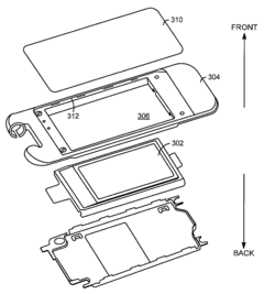
- An ESD shield with an ESD-shielding surface and orthogonally protruding tabs is integrated into the device's housing, providing protection for multiple sides by diverting ESD current through slots and tabs, which are hidden from view, thus maintaining a slim form factor and aesthetic appearance.
Safety Standards and Compliance Requirements
Material jetting electronics enclosures must comply with a comprehensive framework of safety standards to ensure proper protection against electrostatic discharge (ESD), electromagnetic interference (EMI), and fire hazards. The International Electrotechnical Commission (IEC) provides several critical standards, including IEC 61340 for ESD protection requirements and IEC 61000 for electromagnetic compatibility. These standards establish minimum performance criteria for materials used in electronics enclosures, particularly those manufactured through material jetting processes.
For ESD protection, ANSI/ESD S20.20 serves as the primary standard in North America, requiring electronics enclosures to maintain surface resistivity between 1 × 10^4 and 1 × 10^11 ohms to effectively dissipate static charges. Material jetted enclosures must undergo rigorous testing according to ANSI/ESD STM11.11 and STM11.12 to verify their compliance with these resistivity requirements across varying environmental conditions.
Electromagnetic shielding capabilities are governed by IEEE 299 and MIL-STD-461, which mandate specific attenuation levels across different frequency ranges. Material jetted enclosures typically need to demonstrate shielding effectiveness of at least 30dB in the 1-10 GHz range to meet commercial electronics requirements, with more stringent standards applying to military and aerospace applications requiring 60-80dB attenuation.
Flammability compliance represents another critical safety dimension, with UL 94 serving as the predominant standard. Material jetted enclosures for electronics applications must achieve at least a V-0 rating, indicating self-extinguishing properties within 10 seconds after flame removal with no burning drips. The IEC 60695 series provides complementary fire hazard testing methodologies, including glow-wire testing and needle-flame testing protocols specifically relevant to electronics enclosures.
Regional variations in compliance requirements present significant challenges for global manufacturers. The European Union enforces additional requirements through the RoHS Directive (2011/65/EU) and REACH regulations, restricting hazardous substances in electronic equipment. Similarly, Japan's METI standards and China's CCC certification impose region-specific compliance hurdles that material jetted enclosures must overcome.
Testing methodologies for material jetted enclosures require specialized approaches due to their unique manufacturing process. ASTM D257 for volume and surface resistivity measurements must be adapted to account for the layer-by-layer construction and potential anisotropic electrical properties. Similarly, UL 746A for polymeric materials requires modifications to address the distinctive microstructure and potential inclusion of functional additives in material jetted components.
Material Sustainability and Environmental Impact Assessment
The sustainability aspects of material jetting for electronics enclosures represent a critical dimension in evaluating this technology's viability for long-term industrial adoption. Current material jetting processes predominantly utilize photopolymers and thermoplastics that present significant environmental challenges throughout their lifecycle. These materials often derive from petroleum-based sources, contributing to resource depletion and carbon emissions during raw material extraction and processing phases.
Manufacturing energy consumption presents another sustainability concern. Material jetting systems require substantial electrical power for operation, particularly for maintaining precise temperature controls and powering UV curing mechanisms essential for ESD-safe and flame-retardant formulations. This energy intensity translates to considerable carbon footprints when scaled to industrial production volumes.
Waste generation during production constitutes a notable environmental impact factor. Support structures necessary for complex electronics enclosure geometries typically become post-processing waste. Additionally, failed prints and material purging during system transitions generate substantial material waste that often cannot be effectively recycled due to the cross-linked nature of photopolymers used in ESD applications.
End-of-life considerations reveal further challenges. Electronics enclosures with integrated ESD and EMI shielding properties frequently incorporate multiple materials and additives that complicate recycling processes. The composite nature of these specialized materials, particularly those containing metallic fillers for shielding or flame retardants, significantly impedes conventional recycling streams and biodegradability.
Recent advancements show promising developments in bio-based alternatives for material jetting applications. Research into cellulose-derived resins and plant-based monomers demonstrates potential for reducing petroleum dependency while maintaining critical ESD performance parameters. However, these sustainable alternatives currently struggle to match the flame retardancy and EMI shielding capabilities of conventional materials without environmentally problematic additives.
Life Cycle Assessment (LCA) studies comparing material jetted electronics enclosures against traditional manufacturing methods reveal mixed results. While additive manufacturing reduces material waste through design optimization and on-demand production, the environmental impact of specialized materials and energy-intensive processing can offset these advantages. Comprehensive cradle-to-grave analyses indicate that sustainability benefits are highly application-specific and dependent on production volumes, use duration, and end-of-life management strategies.
Unlock deeper insights with Patsnap Eureka Quick Research — get a full tech report to explore trends and direct your research. Try now!
Generate Your Research Report Instantly with AI Agent
Supercharge your innovation with Patsnap Eureka AI Agent Platform!