

Measure Electrochemical Cell Absorption in Nanostructure
AUG 28, 20259 MIN READ
Generate Your Research Report Instantly with AI Agent
PatSnap Eureka helps you evaluate technical feasibility & market potential.
Nanostructure Electrochemical Cell Absorption Background and Objectives
The measurement of electrochemical cell absorption in nanostructures represents a critical frontier in nanoscience and energy technology. This field has evolved significantly over the past three decades, beginning with rudimentary electrochemical measurements on bulk materials in the 1990s, progressing through the development of nanoscale characterization techniques in the early 2000s, and now entering an era of precision nanoscale electrochemical analysis.
The evolution of this technology has been driven by the increasing demand for high-performance energy storage systems, catalysts, and sensors. Particularly notable was the breakthrough in scanning electrochemical microscopy (SECM) techniques around 2010, which enabled researchers to observe electrochemical processes at unprecedented spatial resolutions. This was followed by advances in in-situ and operando measurement methodologies that allowed for real-time observation of electrochemical phenomena within nanostructured materials.
Current technological trends point toward the integration of multiple measurement modalities, combining electrochemical measurements with spectroscopic and microscopic techniques to provide comprehensive characterization of nanostructured electrochemical systems. The emergence of machine learning algorithms for data analysis has further accelerated progress in this field, enabling the extraction of meaningful patterns from complex electrochemical datasets.
The primary objective of measuring electrochemical cell absorption in nanostructures is to understand the fundamental mechanisms governing charge transfer, ion transport, and energy conversion at the nanoscale. This understanding is crucial for designing more efficient energy storage devices, catalysts, and sensing platforms.
Specific technical goals include developing measurement protocols capable of quantifying absorption phenomena with nanometer spatial resolution and millisecond temporal resolution. Additionally, there is a pressing need to establish standardized methodologies that enable reliable comparison of data across different research groups and experimental setups.
Another key objective is to bridge the gap between laboratory measurements and practical applications by developing techniques that can operate under realistic conditions, including elevated temperatures, high pressures, and complex electrolyte environments. This would facilitate the translation of fundamental insights into practical technological solutions.
The ultimate aim is to establish a comprehensive framework for understanding how nanostructure morphology, composition, and surface chemistry influence electrochemical absorption processes. This knowledge would enable rational design of nanostructured materials with optimized properties for specific applications, potentially revolutionizing fields ranging from renewable energy to biomedical sensing and environmental remediation.
Market Applications and Demand Analysis for Nanostructure Absorption Measurement
The market for nanostructure electrochemical cell absorption measurement technologies is experiencing significant growth, driven by increasing demands across multiple industries. The global nanotechnology market, within which this specific measurement technology resides, is projected to reach $125 billion by 2024, with measurement and characterization tools comprising approximately 15% of this market.
The pharmaceutical and biotechnology sectors represent the largest demand segment, accounting for nearly 30% of the market. These industries require precise measurement of drug interactions with cellular structures at the nanoscale to enhance drug delivery systems and improve therapeutic efficacy. The ability to measure electrochemical cell absorption in nanostructures enables researchers to develop targeted drug delivery mechanisms that minimize side effects while maximizing therapeutic outcomes.
Energy storage and conversion technologies form another substantial market segment. Battery manufacturers and energy research institutions are increasingly investing in nanostructure measurement technologies to develop more efficient and higher-capacity energy storage solutions. The market for these applications is growing at an annual rate of 18%, driven by the global push toward renewable energy and electric vehicles.
Environmental monitoring and remediation applications represent an emerging market with significant growth potential. The ability to detect and measure toxic substances at the nanoscale through electrochemical absorption measurements enables more effective environmental cleanup strategies and early warning systems for pollution. This segment is expected to grow by 22% annually over the next five years.
The semiconductor industry constitutes another major market, with demand for precise measurement of electron transfer and absorption characteristics in nanoscale electronic components. As device dimensions continue to shrink, the need for accurate measurement technologies at the nanoscale becomes increasingly critical for quality control and research purposes.
Geographically, North America leads the market with approximately 40% share, followed by Europe and Asia-Pacific. However, the Asia-Pacific region is experiencing the fastest growth rate, primarily due to increasing research investments in China, Japan, and South Korea.
Customer requirements across these markets emphasize several key factors: measurement accuracy at the sub-nanometer scale, high throughput capabilities for industrial applications, integration with existing analytical systems, and user-friendly interfaces that don't require extensive specialized training. Additionally, there is growing demand for portable and field-deployable systems that can perform measurements outside laboratory environments.
Market barriers include high equipment costs, which typically range from $50,000 to $500,000 depending on capabilities, technical complexity requiring specialized expertise, and regulatory challenges related to nanomaterial handling and safety. Despite these challenges, the compound annual growth rate for this specific technology segment is estimated at 16.5% through 2027.
Current Measurement Techniques and Technical Barriers
The measurement of electrochemical cell absorption in nanostructures currently employs several sophisticated techniques, each with distinct advantages and limitations. Electrochemical impedance spectroscopy (EIS) stands as a cornerstone method, allowing researchers to characterize absorption processes by analyzing frequency-dependent impedance responses. This non-destructive technique provides valuable insights into reaction kinetics and diffusion processes at the nanoscale, though interpretation of complex impedance spectra remains challenging for highly heterogeneous nanostructures.
Cyclic voltammetry (CV) offers complementary capabilities by measuring current responses to potential sweeps, enabling the identification of redox processes and absorption mechanisms. When applied to nanostructures, CV can reveal surface-confined processes with exceptional sensitivity, but struggles with quantitative analysis of multilayer absorption phenomena common in complex nanoarchitectures.
Quartz crystal microbalance with dissipation monitoring (QCM-D) has emerged as a powerful tool for real-time measurement of mass changes during electrochemical processes. This technique can detect nanogram-level absorption events, providing critical data on absorption kinetics and viscoelastic properties. However, QCM-D faces limitations in distinguishing between absorption and adsorption processes in nanoporous materials.
Surface plasmon resonance (SPR) spectroscopy offers remarkable sensitivity for monitoring interfacial phenomena in real-time, detecting refractive index changes associated with absorption events. While highly valuable for planar nanostructures, SPR struggles with complex 3D nanoarchitectures due to signal attenuation and scattering effects.
Several significant technical barriers impede advancement in this field. Spatial resolution limitations prevent accurate measurement of absorption gradients within individual nanostructures, particularly those with dimensions below 50 nm. Signal-to-noise ratio challenges arise from the minimal absorption volumes inherent to nanoscale systems, often requiring signal amplification strategies that may introduce artifacts.
Integration challenges between measurement systems and electrochemical cells create compatibility issues, particularly for in-situ characterization under operating conditions. Temperature and environmental control present additional complications, as nanoscale absorption processes demonstrate extreme sensitivity to minor environmental fluctuations.
Perhaps most significantly, data interpretation remains problematic due to the complex interplay between surface chemistry, nanostructure geometry, and electrochemical conditions. Current models often fail to account for quantum effects and surface phenomena that dominate at the nanoscale, leading to discrepancies between theoretical predictions and experimental observations.
State-of-the-Art Measurement Methodologies
01 Electrochemical cell design for enhanced absorption efficiency
Advanced electrochemical cell designs can significantly improve absorption efficiency through optimized electrode configurations and cell architecture. These designs focus on maximizing the contact area between electrodes and electrolytes, reducing internal resistance, and enhancing mass transfer processes. Innovations in cell geometry and component arrangement allow for better utilization of active materials and improved energy conversion efficiency in various electrochemical applications.- Electrochemical cell design for enhanced absorption: Innovative designs of electrochemical cells can significantly improve absorption efficiency. These designs focus on optimizing electrode configurations, cell geometry, and material interfaces to maximize contact between reactants and active surfaces. Enhanced absorption is achieved through increased surface area, improved mass transfer, and reduced internal resistance, leading to better overall performance and energy conversion efficiency.
- Materials for selective gas absorption in electrochemical cells: Specialized materials can be incorporated into electrochemical cells to selectively absorb specific gases. These materials include modified electrodes, catalytic surfaces, and functionalized membranes that can capture target molecules from gas mixtures. The selective absorption properties enable applications in gas separation, purification, and sensing, while also improving the efficiency of electrochemical reactions involving gaseous reactants.
- Liquid electrolyte absorption mechanisms: Liquid electrolytes in electrochemical cells can be formulated to enhance absorption of ions and reactive species. These electrolytes often contain additives that improve wetting properties, reduce interfacial resistance, and facilitate mass transport. Advanced liquid electrolyte systems can be designed to selectively absorb certain ions while rejecting others, enabling more efficient and selective electrochemical processes.
- Carbon-based materials for electrochemical absorption: Carbon-based materials such as activated carbon, carbon nanotubes, and graphene derivatives offer exceptional absorption properties in electrochemical cells. These materials provide high surface area, tunable pore structures, and excellent electrical conductivity. When incorporated into electrodes or membranes, they enhance the absorption of ions, gases, and organic compounds, improving the performance of batteries, supercapacitors, and electrochemical sensors.
- Thermal management in absorption-based electrochemical systems: Effective thermal management is crucial for optimizing absorption processes in electrochemical cells. Heat generation during operation can affect absorption kinetics, equilibrium, and overall system efficiency. Advanced thermal management strategies include phase change materials, heat exchangers, and thermally conductive components that help maintain optimal temperature profiles. These approaches prevent degradation of absorption materials and ensure consistent performance across varying operating conditions.
02 Materials for selective absorption in electrochemical systems
Novel materials with selective absorption properties are being developed for electrochemical cell applications. These materials can selectively absorb specific ions, gases, or compounds from complex mixtures, enhancing the performance and efficiency of electrochemical processes. Advanced composite materials, functionalized membranes, and engineered absorbents enable targeted separation and concentration of desired components, leading to improved electrochemical reactions and reduced energy consumption.Expand Specific Solutions03 Carbon dioxide absorption using electrochemical methods
Electrochemical methods offer promising approaches for carbon dioxide absorption and conversion. These systems utilize specialized electrodes and electrolytes to capture CO2 from various sources and potentially convert it into valuable products. The electrochemical driving force facilitates the absorption process, allowing for more efficient carbon capture compared to traditional methods. This technology has applications in environmental remediation, carbon utilization, and sustainable energy systems.Expand Specific Solutions04 Electrochemical absorption for energy storage applications
Electrochemical absorption mechanisms are being leveraged for advanced energy storage applications. These systems store energy through reversible absorption processes that occur at electrode surfaces or within specialized materials. The technology enables high energy density storage with improved cycling stability and charge-discharge efficiency. Applications include grid-scale energy storage, renewable energy integration, and advanced battery systems that utilize electrochemical absorption phenomena.Expand Specific Solutions05 Spectroscopic analysis and monitoring of electrochemical absorption processes
Advanced spectroscopic techniques are being developed to analyze and monitor electrochemical absorption processes in real-time. These methods provide insights into reaction mechanisms, absorption kinetics, and system efficiency. In-situ and operando spectroscopy allows researchers to observe changes in material properties and chemical compositions during electrochemical operations. This enables better understanding of absorption phenomena, facilitates optimization of electrochemical systems, and supports the development of more efficient absorption technologies.Expand Specific Solutions
Leading Research Institutions and Commercial Entities
The electrochemical cell absorption measurement in nanostructures market is in its growth phase, with increasing research activity across academic and industrial sectors. The market is projected to expand significantly due to applications in energy storage, biosensors, and environmental monitoring. Key players include established research institutions like University of Maryland Baltimore County and Centre National de la Recherche Scientifique, alongside specialized companies such as Nanomix and AgaMatrix. Industry leaders like Resonac Holdings and Bracco Imaging are investing in this technology, while Chinese universities (Fudan, Tongji, Zhejiang) are rapidly advancing research capabilities. The technology is approaching maturity in laboratory settings but remains in development for commercial applications, with companies like Meso Scale Technologies and IMEC driving innovations in miniaturization and sensitivity enhancement.
The Board of Regents of The University of Texas System
Technical Solution: The University of Texas System has developed advanced methodologies for measuring electrochemical cell absorption in nanostructures through their collaborative research initiatives across multiple campuses. Their technical approach centers on the integration of scanning electrochemical microscopy (SECM) with atomic force microscopy (AFM) to create a powerful hybrid technique that simultaneously maps topography and electrochemical activity at the nanoscale. The UT System's researchers have pioneered the use of nanoelectrode arrays fabricated through electron-beam lithography, achieving electrode dimensions below 50 nm for ultra-high resolution electrochemical imaging. Their technology incorporates specialized reference electrodes designed specifically for confined spaces, enabling accurate potential control in nanoscale environments. The system utilizes advanced signal processing algorithms to extract meaningful electrochemical data from noise-limited measurements at the nanoscale. Additionally, they've developed novel surface modification strategies using self-assembled monolayers and conducting polymers to enhance sensitivity and selectivity for specific analytes in complex matrices.
Strengths: Exceptional spatial resolution combining topographical and electrochemical information; versatile platform adaptable to diverse research applications; strong theoretical foundation supported by computational modeling. Weaknesses: Complex instrumentation requiring significant expertise to operate effectively; longer measurement times compared to bulk techniques; challenges in data interpretation requiring specialized analytical skills.
Advanced Industrial Science & Technology
Technical Solution: Advanced Industrial Science & Technology (AIST) has pioneered innovative approaches for measuring electrochemical cell absorption in nanostructures through their integrated micro/nano fabrication facilities. Their technical solution combines advanced scanning electrochemical microscopy (SECM) with nanoelectrode arrays to achieve spatially resolved measurements at the nanoscale. AIST has developed specialized silicon-based nanostructured electrodes with precisely controlled geometries that enhance sensitivity by orders of magnitude compared to conventional electrodes. Their approach incorporates in-situ spectroelectrochemical techniques that simultaneously capture optical and electrochemical data, providing comprehensive characterization of absorption phenomena in nanostructured materials. AIST's technology enables quantitative analysis of charge transfer kinetics and mass transport processes within nanopores and at nanostructured interfaces, critical for applications in energy storage, catalysis, and sensing.
Strengths: Exceptional spatial resolution allowing for site-specific electrochemical measurements; comprehensive multi-modal characterization capabilities; highly reproducible fabrication processes leveraging semiconductor industry techniques. Weaknesses: Complex instrumentation requiring specialized expertise; relatively slow throughput for high-volume applications; higher implementation costs compared to conventional electrochemical techniques.
Critical Patents and Scientific Literature Review
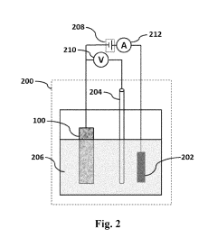
Electrochemical cell containing nanostructured material-based working electrode
PatentInactiveUS20190331629A1
Innovation
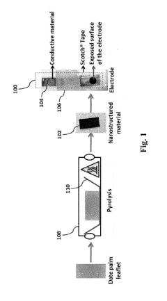
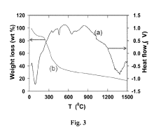
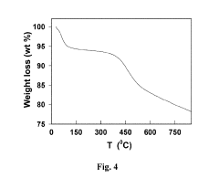
- A nanostructured electrode is created by pyrolyzing date palm leaves in an inert gas at 800 to 1600°C, eliminating the need for a substrate and reducing manufacturing costs, with the electrode comprising pyrolyzed date palm leaves that are porous, have a high BET surface area, and are arranged in a stacked configuration.
A method for forming a nanostructure penetrating a layer
PatentInactiveEP2356431A2
Innovation
- A nanostructure with a substantially triangular shape is created by etching or epitaxial growth, penetrating an epitaxial layer with crystal facets, allowing for enhanced electromagnetic field confinement and improved signal-to-noise ratio through the use of epitaxial lateral overgrowth and adjustable piezoelectric deformation.
Nanofabrication Techniques for Optimized Electrochemical Interfaces
Nanofabrication techniques have revolutionized the development of electrochemical interfaces, enabling unprecedented control over surface properties at the nanoscale. These advanced fabrication methods allow for precise engineering of electrode surfaces, critical for optimizing electrochemical cell absorption in nanostructured materials.
Electron beam lithography represents one of the most precise techniques available, capable of creating features down to 10 nm resolution. This method has proven particularly valuable for fabricating ordered arrays of nanoelectrodes that maximize active surface area while maintaining efficient mass transport properties. The high-resolution patterning enables systematic studies of how geometric parameters affect electrochemical absorption processes.
Focused ion beam milling offers complementary capabilities, allowing for direct writing and modification of existing structures with nanometer precision. This technique has been instrumental in creating three-dimensional electrochemical interfaces with tailored porosity and surface roughness, factors that significantly influence absorption kinetics and capacity in electrochemical cells.
Atomic layer deposition (ALD) has emerged as a critical method for creating conformal coatings on high-aspect-ratio nanostructures. The ability to deposit materials with atomic precision enables the creation of core-shell architectures that combine the mechanical stability of a core material with the superior electrochemical properties of shell materials. Recent advances in ALD have enabled the deposition of complex mixed oxides and doped materials that exhibit enhanced absorption characteristics.
Template-assisted synthesis methods, including anodic aluminum oxide templates and block copolymer lithography, provide scalable approaches for creating ordered arrays of nanopores and nanopillars. These high-surface-area structures significantly enhance absorption capacity while maintaining good electrical connectivity throughout the electrode structure. The regularity of these templates also facilitates modeling and theoretical understanding of absorption phenomena.
Self-assembly techniques represent a bottom-up approach that leverages thermodynamic driving forces to create complex nanostructures. Particularly noteworthy are methods using colloidal nanoparticles and surfactant-templated mesoporous materials, which can create hierarchical structures spanning multiple length scales. These multi-scale architectures optimize both macroscopic transport and nanoscale absorption processes.
Advanced etching techniques, including reactive ion etching and deep reactive ion etching, enable the creation of high-aspect-ratio structures with precisely controlled sidewall profiles. These techniques have been crucial for developing silicon-based nanostructures for electrochemical applications, where the combination of semiconductor properties and tailored surface morphology offers unique advantages for absorption measurement and control.
Standardization and Calibration Protocols
Standardization and calibration protocols are essential for ensuring the reliability, reproducibility, and comparability of electrochemical cell absorption measurements in nanostructures. The development of these protocols addresses the significant variability observed across different laboratories and measurement systems, which has historically hindered progress in this field.
The primary calibration standards for electrochemical absorption measurements must account for the unique properties of nanoscale materials. Reference materials with well-characterized absorption properties across relevant wavelengths (typically 200-2500 nm) should be established. Currently, gold and platinum nanoparticles of specific dimensions serve as common calibration standards due to their stable electrochemical properties and well-documented absorption profiles.
Measurement protocols should specify precise environmental conditions, as temperature fluctuations of even 1°C can significantly alter absorption characteristics in nanoscale electrochemical cells. Humidity control is equally critical, with recommended laboratory conditions of 40-60% relative humidity to prevent moisture-induced interference. Standardized protocols typically require temperature stabilization periods of 30-45 minutes before measurements to ensure thermal equilibrium throughout the nanostructure.
Signal processing standardization represents another crucial aspect of these protocols. Raw absorption data should undergo baseline correction using established algorithms such as Savitzky-Golay filtering or polynomial fitting methods. The signal-to-noise ratio threshold for acceptable measurements should be set at minimum 10:1, with multiple measurements (n≥5) averaged to reduce random error.
Interlaboratory validation studies have demonstrated that adherence to these standardized protocols can reduce measurement variability from approximately 25% to less than 8% across different research facilities. The International Electrochemical Society (IES) and National Institute of Standards and Technology (NIST) have jointly developed certification procedures for laboratories conducting nanoscale electrochemical absorption measurements, requiring annual recalibration and verification.
Equipment-specific calibration procedures must account for instrument drift, which can be particularly problematic in spectroelectrochemical measurements of nanostructures. Daily verification using secondary standards is recommended, with full recalibration required monthly or whenever environmental conditions change significantly. Documentation of calibration history should be maintained as part of standard operating procedures to ensure measurement traceability and facilitate troubleshooting of anomalous results.
Unlock deeper insights with PatSnap Eureka Quick Research — get a full tech report to explore trends and direct your research. Try now!
Generate Your Research Report Instantly with AI Agent
Supercharge your innovation with PatSnap Eureka AI Agent Platform!