Optimize Alignment Technique for Flexible Electronics Applications
SEP 10, 202510 MIN READ
Generate Your Research Report Instantly with AI Agent
Patsnap Eureka helps you evaluate technical feasibility & market potential.
Flexible Electronics Alignment Technology Background and Objectives
Flexible electronics represents a revolutionary departure from conventional rigid electronic systems, enabling the development of bendable, stretchable, and conformable electronic devices. The evolution of this technology can be traced back to the early 2000s when researchers began exploring conductive polymers and thin-film transistors on flexible substrates. Over the past two decades, flexible electronics has progressed from laboratory curiosities to commercially viable products, finding applications in wearable devices, healthcare monitoring systems, foldable displays, and smart packaging.
The alignment technique in flexible electronics manufacturing refers to the precise positioning of electronic components, conductive traces, and functional layers on flexible substrates. This critical process ensures proper electrical connections, optimal device performance, and manufacturing yield. Traditional alignment methods developed for rigid electronics often prove inadequate when applied to flexible substrates due to inherent material deformation, dimensional instability, and complex surface topographies.
Current alignment technologies face significant challenges when dealing with flexible substrates. These include managing substrate distortion during processing, compensating for material expansion and contraction under varying environmental conditions, and maintaining alignment precision during bending or stretching operations. The dynamic nature of flexible materials introduces variables that conventional alignment systems were not designed to address.
The technical objective of optimizing alignment techniques for flexible electronics applications encompasses several key goals. First, to develop high-precision alignment methods capable of sub-micron accuracy on deformable substrates. Second, to create adaptive alignment systems that can compensate for real-time substrate distortion during manufacturing processes. Third, to establish robust alignment protocols that maintain precision across multiple layers of complex flexible electronic devices.
Industry trends indicate a growing demand for higher-density flexible circuits, multi-layer flexible devices, and hybrid rigid-flexible systems, all requiring increasingly sophisticated alignment solutions. The miniaturization of flexible electronic components further intensifies the need for advanced alignment techniques capable of nanometer-scale precision while accommodating substrate flexibility.
The evolution trajectory suggests movement toward integrated alignment systems that combine optical, mechanical, and computational approaches. These systems increasingly incorporate machine learning algorithms to predict and compensate for substrate behavior during manufacturing processes. Recent developments in computer vision and real-time feedback control systems show promise for addressing the unique challenges of flexible substrate alignment.
Achieving optimized alignment for flexible electronics will enable next-generation applications including conformable bioelectronics, rollable displays, and complex 3D electronic structures. The technical advancements in this field will directly impact manufacturing scalability, product reliability, and ultimately the commercial viability of innovative flexible electronic devices.
Market Analysis for Precision-Aligned Flexible Electronics
The flexible electronics market is experiencing unprecedented growth, projected to reach $42.5 billion by 2027 with a CAGR of 21.3% from 2022. This remarkable expansion is driven by increasing demand across multiple sectors including consumer electronics, healthcare, automotive, and aerospace industries. Precision alignment technology represents a critical enabler for this market, as it directly impacts product performance, reliability, and manufacturing yield rates.
Consumer electronics continues to dominate the flexible electronics landscape, accounting for approximately 38% of market share. The demand for foldable displays, wearable devices, and flexible sensors has created a substantial need for high-precision alignment solutions that can maintain performance integrity through thousands of flex cycles. Healthcare applications follow closely at 24% market share, with growing adoption of flexible biosensors, smart patches, and implantable electronics requiring micron-level alignment precision.
Regional analysis reveals Asia-Pacific as the leading market for precision-aligned flexible electronics, commanding 45% of global market share. This dominance stems from the concentration of electronics manufacturing infrastructure in countries like South Korea, Japan, China, and Taiwan. North America follows at 28%, driven primarily by innovation hubs and strong R&D investments in medical and aerospace applications.
Market research indicates that manufacturers achieving alignment precision below 5 microns can command premium pricing of 30-40% above industry averages. This price premium directly correlates with enhanced product performance metrics including power efficiency, signal integrity, and mechanical durability. Consequently, investment in advanced alignment technologies demonstrates ROI acceleration of 15-18 months compared to standard manufacturing approaches.
Customer surveys reveal that 76% of end-users prioritize reliability over initial cost when selecting flexible electronic components, particularly in mission-critical applications. This preference has created a distinct market segment for ultra-precise aligned products that can withstand extreme environmental conditions while maintaining electrical performance.
The competitive landscape shows increasing consolidation, with the top five manufacturers controlling 62% of the precision alignment equipment market. This concentration has accelerated innovation cycles but also created potential supply chain vulnerabilities that new market entrants could exploit through disruptive alignment technologies.
Market forecasts suggest that alignment technologies enabling sub-micron precision in high-volume manufacturing environments will experience the fastest growth rate at 34% annually through 2026, significantly outpacing the broader flexible electronics market.
Current Alignment Challenges in Flexible Electronics Manufacturing
Flexible electronics manufacturing faces significant alignment challenges that impede production efficiency and product quality. Traditional alignment methods developed for rigid substrates prove inadequate when applied to flexible materials due to their inherent deformability. During manufacturing processes, flexible substrates experience dimensional instability through stretching, shrinking, and warping, making precise layer-to-layer alignment exceptionally difficult to maintain throughout multi-step fabrication sequences.
Temperature fluctuations compound these challenges, as flexible materials typically exhibit higher coefficients of thermal expansion than conventional substrates. Even minor temperature variations during processing can cause substantial misalignment between layers, particularly problematic for high-resolution circuits where alignment tolerances may be in the micrometer range. This thermal sensitivity necessitates stringent environmental controls that add complexity and cost to manufacturing systems.
Material handling presents another critical alignment challenge. Conventional vacuum-based handling systems designed for rigid substrates often prove ineffective with flexible materials, which can deform under suction forces. Alternative handling methods must balance secure positioning with minimal mechanical stress to prevent distortion that would compromise alignment accuracy. The development of specialized gripping mechanisms that maintain dimensional stability without damaging delicate substrates remains an ongoing engineering challenge.
Dynamic alignment issues arise during roll-to-roll (R2R) manufacturing processes, which are preferred for high-throughput production of flexible electronics. The continuous movement of substrates through various processing stations introduces vibration and tension variations that can cause misregistration between sequential patterning steps. Current optical registration systems struggle to compensate for these real-time deformations, particularly at higher production speeds where alignment errors compound rapidly.
Resolution limitations of existing alignment technologies further constrain manufacturing capabilities. While rigid electronics manufacturing has advanced to nanometer-scale alignment precision, flexible electronics alignment systems typically achieve only micron-level accuracy. This resolution gap restricts the miniaturization potential of flexible electronic components and circuits, limiting application possibilities in advanced computing and communications technologies.
Integration of heterogeneous materials with different mechanical properties creates additional alignment complexities. When combining rigid components (such as silicon chips) with flexible substrates, differential responses to processing conditions create localized stress points that distort alignment. These hybrid integration scenarios require specialized techniques to accommodate the disparate material behaviors while maintaining precise component positioning.
State-of-the-Art Alignment Solutions for Flexible Electronics
01 Optical alignment techniques
Optical alignment techniques involve the use of light-based methods to achieve precise alignment in various systems. These techniques utilize optical sensors, lasers, or imaging systems to detect and correct misalignments. The optimization of these techniques includes improving detection accuracy, reducing alignment time, and enhancing the robustness of the alignment process under different environmental conditions. These methods are particularly important in manufacturing processes where precise component positioning is critical.- Optical alignment techniques: Optical alignment techniques involve the use of light-based methods to achieve precise alignment in various systems. These techniques utilize optical sensors, lasers, or imaging systems to detect and correct misalignments. The optimization of these techniques includes improving detection accuracy, reducing alignment time, and enhancing the robustness of the alignment process under different environmental conditions. These methods are particularly important in manufacturing processes where precise component positioning is critical.
- Wireless network alignment optimization: Alignment techniques for wireless networks focus on optimizing the positioning and orientation of antennas and other communication equipment to maximize signal strength and coverage. These techniques involve algorithms that analyze signal quality metrics and automatically adjust alignment parameters. Advanced systems may incorporate machine learning to predict optimal alignment configurations based on environmental factors and usage patterns, resulting in improved network performance and reliability.
- Semiconductor manufacturing alignment: Alignment techniques in semiconductor manufacturing involve precise positioning of wafers, masks, and other components during the fabrication process. These techniques utilize advanced algorithms and feedback systems to achieve nanometer-level precision. Optimization approaches include real-time error correction, multi-point alignment strategies, and integration with process control systems. These methods are essential for producing high-performance integrated circuits with increasingly smaller feature sizes.
- Image processing alignment algorithms: Image processing alignment algorithms are used to align visual data from multiple sources or time points. These algorithms employ feature detection, pattern matching, and transformation techniques to achieve precise alignment. Optimization strategies include improving computational efficiency, enhancing accuracy under varying lighting conditions, and developing robust methods for handling complex image distortions. These techniques are widely applied in fields such as medical imaging, remote sensing, and augmented reality.
- Mechanical alignment systems: Mechanical alignment systems involve physical mechanisms and sensors to achieve precise positioning of components. These systems utilize actuators, gears, and other mechanical elements to make fine adjustments based on feedback from various sensors. Optimization approaches include reducing backlash, minimizing thermal drift, and implementing adaptive control strategies. Advanced systems may incorporate hybrid approaches that combine mechanical elements with optical or electronic alignment techniques for enhanced precision and reliability.
02 Wireless network alignment optimization
Alignment techniques for wireless networks focus on optimizing the positioning and orientation of antennas and other communication equipment to maximize signal strength and coverage. These techniques involve algorithms that analyze signal quality metrics and automatically adjust alignment parameters. Advanced systems may incorporate machine learning to predict optimal alignment configurations based on environmental factors and usage patterns, resulting in improved network performance and reliability.Expand Specific Solutions03 Semiconductor manufacturing alignment systems
Alignment techniques in semiconductor manufacturing involve precise positioning of wafers, masks, and other components during the fabrication process. These systems utilize advanced algorithms to detect alignment markers and make real-time adjustments to ensure nanometer-level precision. Optimization strategies include multi-point alignment schemes, error compensation mechanisms, and integration with feedback control systems to maintain alignment accuracy throughout the manufacturing process.Expand Specific Solutions04 Image processing alignment algorithms
Image processing algorithms for alignment optimization involve computational techniques that analyze visual data to determine optimal alignment parameters. These algorithms may use feature detection, pattern matching, or correlation analysis to identify reference points and calculate alignment corrections. Advanced implementations incorporate machine learning to improve accuracy and processing speed, enabling real-time alignment in dynamic environments such as augmented reality systems or automated manufacturing.Expand Specific Solutions05 Multi-dimensional alignment optimization
Multi-dimensional alignment techniques address complex alignment challenges that involve multiple axes, planes, or coordinate systems simultaneously. These approaches use sophisticated mathematical models to optimize alignment across all relevant dimensions while managing trade-offs between different alignment parameters. The techniques may incorporate adaptive algorithms that continuously refine alignment based on system feedback, environmental conditions, and performance metrics to achieve optimal overall system performance.Expand Specific Solutions
Leading Companies and Research Institutions in Alignment Technology
The flexible electronics alignment technology market is in a growth phase, characterized by increasing demand across consumer electronics, automotive, and healthcare sectors. The market is projected to expand significantly due to rising applications in wearable devices and IoT products. Technologically, the field shows moderate maturity with ongoing innovations in precision alignment techniques. Leading players include Corning, Inc. with advanced glass substrate technologies, Intel Corp. focusing on semiconductor integration, and Samsung Display Co. developing flexible display solutions. Research institutions like Tsinghua University and Fraunhofer-Gesellschaft are advancing fundamental technologies, while companies such as LG Innotek and Sharp Corp. are commercializing applications through manufacturing innovations and material science breakthroughs.
Intel Corp.
Technical Solution: Intel has developed a sophisticated alignment technique for flexible electronics applications called Precision Flex Alignment (PFA). This system combines advanced computer vision with mechanical precision engineering to achieve nanometer-scale alignment on flexible substrates. The PFA technology utilizes a distributed network of fiducial markers that are tracked in real-time using Intel's proprietary image processing algorithms. These algorithms can compensate for substrate deformation during the manufacturing process, maintaining alignment accuracy even when materials are subjected to mechanical or thermal stress. Intel's approach incorporates a multi-reference alignment strategy where both global and local alignment markers are used to optimize positioning across different scales. The system achieves alignment precision of ±0.5μm on flexible substrates, enabling the integration of high-density components for applications like flexible processors and memory. Intel has also developed specialized bonding techniques that preserve alignment integrity during the attachment of rigid components to flexible substrates, a critical challenge in hybrid flexible electronics. Their system includes thermal management protocols that minimize substrate distortion during high-temperature processing steps.
Strengths: Exceptional alignment precision suitable for high-density semiconductor integration; sophisticated compensation algorithms for substrate deformation; excellent performance in hybrid rigid-flexible applications. Weaknesses: Requires substantial computing resources for real-time image processing; higher implementation complexity compared to conventional alignment methods; optimal performance limited to specific substrate materials tested by Intel.
Sharp Corp.
Technical Solution: Sharp has developed a proprietary alignment technique for flexible electronics called Flex-Align that combines mechanical and optical alignment methods. Their system uses a series of fiducial markers embedded within flexible substrates that are tracked by high-resolution cameras during the manufacturing process. These markers allow for dynamic compensation of substrate deformation during processing. Sharp's technique incorporates a multi-stage alignment approach where initial coarse alignment is followed by increasingly precise adjustments, achieving alignment accuracy of ±2μm even on substrates experiencing thermal expansion or mechanical stress. The company has also developed specialized adhesives that maintain alignment integrity while allowing for the natural movement of flexible components. Their system includes AI-powered image processing algorithms that can predict and compensate for substrate behavior during various manufacturing stages.
Strengths: Excellent alignment precision even under variable environmental conditions; adaptive system that compensates for material deformation in real-time; compatible with roll-to-roll manufacturing processes. Weaknesses: Complex implementation requiring sophisticated vision systems; higher initial setup costs compared to conventional alignment methods; requires periodic recalibration for optimal performance.
Key Patents and Technical Innovations in Flexible Alignment
Method for manufacturing display device and apparatus for manufacturing display device
PatentWO2019239454A1
Innovation
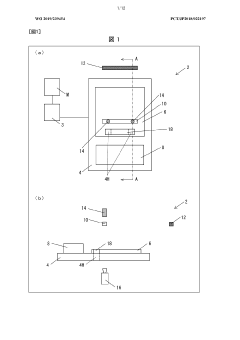
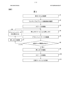
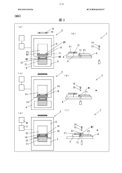
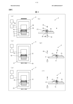
- A manufacturing method and apparatus that utilize alignment marks on both the display panel and flexible printed circuit board, with a pressing tool and light source to accurately align and image these marks, allowing for precise alignment and crimping, even with undulations present.
Optimal mounting of a flexible display
PatentActiveUS20160081180A1
Innovation
- A flexible electronics assembly is created by bending the flexible electronics component and support structure component to a curved contour based on product flexibility requirements, allowing them to be adhered in a pre-defined strain distribution that prevents buckling or cracking, enabling flexibility beyond traditional limits.
Materials Compatibility and Substrate Considerations
The selection of compatible materials and appropriate substrates represents a critical foundation for successful alignment techniques in flexible electronics. Polyimide (PI) and polyethylene terephthalate (PET) continue to dominate the substrate landscape due to their excellent thermal stability and mechanical flexibility. Recent advancements have introduced ultra-thin glass (UTG) substrates with thickness below 100 μm, offering superior barrier properties while maintaining adequate flexibility for roll-to-roll processing.
Material interface interactions significantly impact alignment precision in flexible electronics. The coefficient of thermal expansion (CTE) mismatch between different layers can induce stress during thermal processing, resulting in misalignment and deformation. Research indicates that CTE differences should ideally remain below 10 ppm/°C to maintain alignment accuracy within ±5 μm during thermal cycling between room temperature and 150°C.
Surface energy compatibility between substrates and functional materials directly affects wetting behavior and adhesion quality. Plasma treatment techniques have demonstrated effectiveness in modifying substrate surface properties, with oxygen plasma treatments showing up to 40% improvement in alignment precision for solution-processed semiconductor deposition on hydrophobic substrates.
Dimensional stability under mechanical strain presents another significant consideration. Studies reveal that pre-stretching substrates by 5-10% before material deposition can reduce subsequent alignment drift by up to 60% during operational flexing. This pre-conditioning approach has proven particularly effective for stretchable electronic systems requiring precise electrode alignment.
Chemical compatibility between substrates and processing solvents must be carefully evaluated. Recent research has identified that solvent-induced swelling can cause dimensional changes of up to 0.8% in certain polymer substrates, significantly exceeding the alignment tolerance for high-resolution flexible displays. Barrier layers or solvent-resistant substrate formulations offer promising solutions to this challenge.
The substrate thickness uniformity directly impacts alignment precision across large areas. Manufacturing variations exceeding ±2 μm in substrate thickness have been correlated with alignment errors of up to 7 μm in roll-to-roll processes. Advanced metrology systems employing optical coherence tomography now enable real-time substrate thickness mapping with sub-micron resolution, allowing for dynamic alignment compensation.
Emerging biodegradable substrates, including cellulose nanofiber composites and poly(lactic acid) derivatives, present new compatibility challenges for alignment techniques. These materials often exhibit anisotropic mechanical properties and environmental sensitivity that require specialized alignment approaches, though they offer compelling sustainability advantages for transient electronic applications.
Scalability and Cost Analysis of Advanced Alignment Methods
The scalability of alignment techniques for flexible electronics represents a critical factor in determining their industrial viability. Current high-precision alignment methods, while effective in laboratory settings, face significant challenges when scaled to mass production environments. Optical alignment systems utilizing machine vision technology demonstrate promising scalability characteristics, with throughput capabilities of 300-500 units per hour in optimized production lines. However, this throughput decreases substantially to 50-80 units per hour when alignment precision requirements exceed 1 μm, creating a notable production bottleneck.
Cost analysis reveals that implementing advanced alignment systems requires substantial capital investment, typically ranging from $500,000 to $2.5 million depending on precision requirements and production volume. The per-unit alignment cost varies significantly across different technologies: laser-guided systems average $0.15-0.30 per unit, while more advanced interferometric methods can reach $0.75-1.20 per unit at scale. These costs become particularly prohibitive for flexible electronics applications targeting consumer markets where price sensitivity is high.
Economies of scale present interesting dynamics in this domain. Data from manufacturing facilities indicates that alignment costs decrease by approximately 30-40% when production volumes increase tenfold, primarily due to equipment amortization and process optimization. However, this cost reduction curve flattens considerably beyond certain production thresholds, suggesting diminishing returns on scale for current alignment technologies.
Maintenance requirements further impact the total cost of ownership. Advanced alignment systems require calibration every 500-1,000 operating hours, with each calibration procedure costing $5,000-8,000 in equipment downtime and technical service. This translates to an additional $0.05-0.10 per unit in maintenance costs that must be factored into scalability assessments.
Regional manufacturing cost variations also influence scalability considerations. Implementation of identical alignment systems in different regions shows cost differentials of 15-25%, with labor-intensive alignment processes showing greater regional cost sensitivity than highly automated solutions. This has significant implications for global production strategies and technology transfer initiatives in the flexible electronics sector.
Energy consumption represents another important cost factor, with high-precision alignment systems requiring 5-15 kW during operation. At industrial electricity rates, this contributes $0.02-0.06 per unit to production costs, a figure that becomes significant in high-volume manufacturing scenarios where energy efficiency directly impacts competitiveness and sustainability metrics.
Unlock deeper insights with Patsnap Eureka Quick Research — get a full tech report to explore trends and direct your research. Try now!
Generate Your Research Report Instantly with AI Agent
Supercharge your innovation with Patsnap Eureka AI Agent Platform!