Optimizing Cost-per-Lumen in Mini LED Manufacturing
SEP 15, 20259 MIN READ
Generate Your Research Report Instantly with AI Agent
Patsnap Eureka helps you evaluate technical feasibility & market potential.
Mini LED Technology Background and Objectives
Mini LED technology represents a significant advancement in display technology, bridging the gap between traditional LED backlighting and the more advanced Micro LED displays. Emerging in the mid-2010s, Mini LEDs are characterized by their size ranging from 100 to 200 micrometers, substantially smaller than conventional LEDs but larger than Micro LEDs. This technology has evolved from the continuous pursuit of enhanced display performance, particularly in terms of contrast ratio, brightness, and energy efficiency.
The evolution of Mini LED technology has been driven by the limitations of traditional LCD displays, which often struggle with achieving deep blacks and high contrast ratios. By incorporating thousands of tiny LEDs as backlighting units, Mini LED displays can achieve more precise local dimming, resulting in improved contrast and color accuracy. This advancement has positioned Mini LED as a viable alternative to OLED technology, especially in scenarios requiring high brightness and durability.
The global display market has witnessed a significant shift towards Mini LED adoption across various applications, including televisions, monitors, laptops, and automotive displays. Major electronics manufacturers have increasingly integrated this technology into their premium product lines, signaling a growing market confidence in its capabilities and future potential.
The primary technical objective in Mini LED manufacturing is optimizing the cost-per-lumen ratio, which represents the economic efficiency of light output. This metric is crucial as it directly impacts the commercial viability of Mini LED displays in competitive consumer electronics markets. Current manufacturing processes face challenges related to yield rates, chip transfer efficiency, and production scalability, all of which contribute to higher costs per unit of light output.
Reducing the cost-per-lumen involves addressing several interconnected technical challenges: improving the efficiency of LED chips themselves, enhancing the manufacturing processes to increase yield rates, developing more cost-effective packaging solutions, and optimizing the optical design to maximize light extraction and utilization. These objectives require advancements in materials science, precision engineering, and production automation.
The trajectory of Mini LED technology development indicates a clear trend toward higher integration density, improved energy efficiency, and reduced manufacturing costs. Industry projections suggest that continued research and development efforts will likely result in significant cost reductions over the next five years, potentially expanding the technology's market penetration beyond premium segments.
As display technologies continue to evolve, Mini LED stands at a critical juncture where technical innovation must align with economic feasibility. The ultimate goal is to establish Mini LED as a mainstream display technology that offers superior visual performance while maintaining competitive pricing against alternative technologies such as OLED and conventional LCD displays.
Market Demand Analysis for Mini LED Applications
The Mini LED market is experiencing robust growth driven by increasing demand for high-quality display technologies across multiple sectors. Current market analysis indicates that the global Mini LED market is projected to reach $5.9 billion by 2025, growing at a CAGR of 86.6% from 2020. This exceptional growth trajectory is primarily fueled by the technology's superior performance characteristics compared to traditional LED and OLED alternatives.
Consumer electronics represents the largest application segment, with premium televisions and high-end monitors leading adoption. Major manufacturers including Samsung, LG, and TCL have already launched Mini LED backlit products, reporting significant sales increases in their premium display categories. The automotive sector follows as the second-largest market, where Mini LED technology is being integrated into advanced dashboard displays, infotainment systems, and ambient lighting solutions.
Market research reveals that consumers are increasingly willing to pay premium prices for displays offering enhanced brightness, better contrast ratios, and improved energy efficiency. This consumer preference creates a favorable environment for Mini LED technology, which delivers these benefits while maintaining competitive pricing compared to OLED alternatives.
Regional analysis shows Asia-Pacific dominating the market with approximately 45% share, driven by the concentration of display manufacturing infrastructure in countries like Taiwan, China, and South Korea. North America follows with 30% market share, characterized by high consumer spending power and early technology adoption.
The cost-per-lumen metric is particularly critical in this expanding market. Current industry benchmarks indicate that Mini LED solutions average $0.05-0.08 per lumen, representing a significant improvement over previous generations but still higher than traditional LED technologies. Market research indicates that achieving a cost-per-lumen threshold of $0.03 would trigger mass market adoption across mid-range consumer products.
Supply chain analysis reveals growing pressure on manufacturers to optimize production costs while maintaining quality standards. Component suppliers report increasing orders for Mini LED chips, with epistar, San'an Optoelectronics, and Nichia Corporation expanding production capacity to meet projected demand.
Market forecasts suggest that as manufacturing processes mature and economies of scale improve, the cost-per-lumen for Mini LED technology will decrease by approximately 15% annually over the next three years. This cost reduction is essential to expand market penetration beyond premium segments and compete effectively with emerging display technologies.
Technical Challenges in Mini LED Manufacturing
Mini LED manufacturing faces several significant technical challenges that impact the optimization of cost-per-lumen metrics. The primary challenge lies in the mass transfer process, where thousands of tiny LED chips must be precisely placed onto substrates. Current pick-and-place technologies struggle with throughput limitations when handling chips smaller than 100 micrometers, creating a bottleneck in production efficiency.
Yield management represents another critical challenge, as defects in Mini LED chips significantly impact overall panel performance. The industry currently experiences yield rates between 70-85%, substantially lower than mature LCD manufacturing processes that achieve over 95%. Each defective chip not only represents direct material waste but also requires costly rework or results in downgraded final products.
Thermal management poses substantial engineering difficulties as Mini LEDs operate at high current densities. Without proper thermal dissipation, these devices experience accelerated degradation and color shift. Current thermal interface materials and heat sink designs add considerable cost while not fully resolving heat concentration issues in ultra-thin display applications.
Driving circuit complexity increases exponentially with Mini LED implementations. Unlike conventional LED backlights with dozens of control zones, Mini LED displays require thousands of independently controlled zones to achieve their superior contrast ratios. This necessitates sophisticated local dimming algorithms and high-density circuit designs that significantly impact manufacturing costs and yield rates.
Chip miniaturization presents fundamental physical challenges. As manufacturers push toward smaller chip dimensions to increase pixel density and reduce costs, quantum efficiency tends to decrease due to increased surface-to-volume ratios and edge effects. Current epitaxial growth and chip fabrication processes struggle to maintain consistent performance at dimensions below 50 micrometers.
Optical efficiency optimization remains problematic as light extraction from Mini LEDs and subsequent color conversion through quantum dot or phosphor layers introduces significant losses. Current designs typically achieve only 40-60% optical efficiency from chip to final emitted light, representing substantial energy waste and reduced luminous efficacy.
Testing and binning processes become increasingly complex and time-consuming with Mini LED technology. Each panel may contain tens of thousands of chips that must be individually tested for brightness and color consistency, requiring sophisticated automated optical inspection systems that add significant capital equipment costs to the manufacturing process.
Current Cost Reduction Approaches in Mini LED Production
01 Manufacturing cost reduction techniques for Mini LED displays
Various manufacturing techniques have been developed to reduce the cost-per-lumen of Mini LED displays. These include optimized production processes, improved assembly methods, and innovative substrate materials that allow for more efficient light emission. By streamlining the manufacturing process and reducing material waste, manufacturers can significantly lower the cost while maintaining or improving luminous output, thereby enhancing the cost-per-lumen ratio.- Manufacturing cost reduction techniques for Mini LED displays: Various manufacturing techniques have been developed to reduce the cost-per-lumen of Mini LED displays. These include optimized production processes, improved assembly methods, and innovative substrate materials that allow for more efficient light emission. By streamlining the manufacturing process and reducing material waste, manufacturers can significantly lower the cost while maintaining or improving luminous output, thereby enhancing the cost-per-lumen ratio.
- Thermal management solutions for Mini LED efficiency: Effective thermal management is crucial for maintaining Mini LED efficiency and longevity, which directly impacts cost-per-lumen metrics. Advanced heat dissipation structures, thermal interface materials, and cooling systems help prevent performance degradation due to heat buildup. These solutions enable Mini LEDs to operate at optimal temperatures, maximizing light output while minimizing power consumption, thereby improving the cost-effectiveness of the lighting solution over its operational lifetime.
- Circuit design optimization for power efficiency: Innovative circuit designs for Mini LED applications focus on improving power efficiency to enhance the cost-per-lumen ratio. These designs include advanced driving circuits, voltage regulation systems, and current distribution networks that minimize energy loss. By optimizing the electrical components that power Mini LEDs, manufacturers can achieve higher luminous efficacy, reducing operational costs and improving the overall value proposition of Mini LED technology.
- Optical enhancement technologies for increased light output: Various optical enhancement technologies have been developed to increase the light output of Mini LEDs without proportionally increasing costs. These include specialized lens designs, reflective materials, light guide structures, and phosphor configurations that improve light extraction and distribution. By maximizing the usable light from each Mini LED element, these technologies effectively reduce the cost-per-lumen by getting more illumination from the same number of LED components.
- Integration of Mini LEDs in display backlight systems: The integration of Mini LEDs in display backlight systems presents unique opportunities for cost-per-lumen optimization. Techniques include local dimming architectures, zone-based illumination control, and hybrid backlight systems that combine Mini LEDs with other technologies. These approaches allow for precise control of brightness in specific display areas, reducing power consumption while maintaining high luminance where needed, thereby improving the overall efficiency and cost-effectiveness of the display system.
02 Thermal management solutions for Mini LED efficiency
Effective thermal management is crucial for maintaining Mini LED efficiency and longevity, which directly impacts cost-per-lumen metrics. Advanced heat dissipation designs, including specialized heat sinks, thermal interface materials, and cooling structures, help prevent performance degradation due to heat buildup. These solutions enable Mini LEDs to operate at optimal temperatures, maximizing light output while extending operational lifespan, thus improving the overall cost-per-lumen value over the product lifecycle.Expand Specific Solutions03 Optical design improvements for enhanced light extraction
Innovations in optical design have significantly improved light extraction efficiency in Mini LED systems. These include advanced lens configurations, reflective materials, and light guide structures that maximize the usable light output from each LED. By increasing the percentage of generated light that actually reaches the intended target, these designs effectively lower the cost-per-lumen by getting more usable illumination from the same power input and LED components.Expand Specific Solutions04 Power efficiency enhancements in Mini LED driver circuits
Advancements in driver circuit design have substantially improved the power efficiency of Mini LED systems. These innovations include optimized current regulation, dynamic power management, and intelligent dimming controls that reduce energy consumption while maintaining brightness levels. By decreasing the power required to achieve the same luminous output, these driver technologies effectively lower the operational cost component of the cost-per-lumen metric, making Mini LED solutions more economically viable for various applications.Expand Specific Solutions05 Material innovations for improved Mini LED performance
Novel materials and substrate technologies have been developed to enhance Mini LED performance and reduce costs. These include advanced semiconductor compounds, improved phosphor materials, and innovative electrode designs that increase quantum efficiency and light output. By improving the fundamental light-generating capabilities of each Mini LED element, these material innovations allow manufacturers to achieve higher lumens per watt, directly improving the cost-per-lumen ratio and making Mini LED technology more competitive in the lighting and display markets.Expand Specific Solutions
Key Industry Players and Competitive Landscape
The Mini LED manufacturing market is currently in a growth phase, characterized by increasing adoption in high-end displays and backlighting applications. The global market size is expanding rapidly, projected to reach significant scale as manufacturers seek to bridge traditional LED and emerging MicroLED technologies. From a technical maturity perspective, companies like BOE Technology, APT Electronics, and TCL's China Star Optoelectronics are leading innovation in cost-per-lumen optimization through advanced manufacturing processes. Taiwanese players including Lextar Electronics and Entire Technology contribute specialized expertise in optical materials and packaging efficiency. The competitive landscape features both established display manufacturers and specialized LED producers working to overcome production yield challenges, reduce chip size while maintaining luminance, and develop more efficient phosphor conversion techniques to drive down the cost-per-lumen metric.
BOE Technology Group Co., Ltd.
Technical Solution: BOE has developed an advanced Mini LED manufacturing process that integrates chip-scale packaging (CSP) technology with mass transfer techniques. Their solution employs a proprietary "active matrix" driving method that allows for precise control of thousands of Mini LED zones. BOE's cost optimization strategy focuses on improving yield rates through automated optical inspection systems that can detect defects at early production stages. They've implemented a multi-chip transfer process that can place up to 1,000 Mini LED chips simultaneously, significantly reducing assembly time and labor costs. Additionally, BOE utilizes phosphor-converted blue LEDs rather than RGB combinations to reduce manufacturing complexity while maintaining color performance.
Strengths: Industry-leading mass transfer technology enables higher throughput and lower per-unit costs. Vertical integration from chip production to display assembly provides better supply chain control. Weaknesses: Higher initial capital investment required for proprietary equipment, potentially limiting flexibility to adapt to rapid technology changes.
Wuhan China Star Optoelectronics Technology Co., Ltd.
Technical Solution: Wuhan China Star (CSOT) has developed a comprehensive Mini LED manufacturing solution called "Ultra-Efficiency Transfer" that addresses cost-per-lumen optimization through multiple approaches. Their technology employs a parallel transfer process capable of handling up to 3,000 chips simultaneously, dramatically reducing assembly time and associated labor costs. CSOT utilizes a proprietary epitaxial structure with enhanced quantum wells that improves internal quantum efficiency by approximately 22% compared to standard designs. Their manufacturing process incorporates an automated defect detection system that uses machine learning algorithms to identify potential failure points before final assembly, significantly improving yield rates. Additionally, CSOT has implemented a novel current spreading layer design that enables more uniform current distribution across the chip surface, resulting in better light output uniformity and reduced hot spots that can lead to premature failure.
Strengths: Highly automated production lines reduce labor costs and human error. Advanced epitaxial designs provide superior efficiency, reducing power consumption and heat generation. Weaknesses: Relatively new to Mini LED mass production compared to some competitors, still optimizing processes for maximum yield.
Core Patents and Innovations in Mini LED Manufacturing
Light-emitting device, backlight plate and display panel
PatentPendingCN118712309A
Innovation
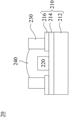
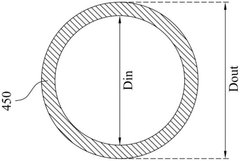
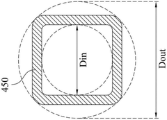
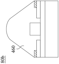
- A light-emitting device is designed, which includes a substrate, a conductive layer, a first reflective layer, a light-emitting element, a second reflective layer and an encapsulation layer. By accurately controlling the difference between the outer diameter and the inner diameter of the second reflective layer (0.05mm to 0.6 mm) and the height relationship of the packaging layer, optimize the packaging structure to reduce light loss and improve stability.
Light emitting diode chip and method of manufacturing the same, and display device
PatentPendingUS20240339575A1
Innovation
- A light emitting diode chip design featuring a base substrate with multiple light emitting structures connected in series, including a current spreading layer and via holes in the insulation layer, which reduces current density and enhances optical performance by optimizing the light emitting area and electrical connections.
Supply Chain Optimization Strategies
Supply chain optimization represents a critical factor in reducing the cost-per-lumen metric in Mini LED manufacturing. Effective supply chain management can significantly impact overall production costs while maintaining quality standards essential for competitive positioning in the display technology market.
Strategic sourcing of key components presents the first optimization opportunity. By establishing long-term partnerships with multiple qualified suppliers of critical materials such as LED chips, substrates, and phosphor materials, manufacturers can negotiate volume-based pricing while ensuring supply continuity. Implementing vendor-managed inventory systems with these partners further reduces carrying costs and minimizes production disruptions.
Vertical integration strategies merit serious consideration for Mini LED manufacturers seeking cost advantages. Companies that control multiple stages of the production process—from chip fabrication to packaging and module assembly—can eliminate markup costs between supply chain tiers. This approach also facilitates tighter quality control and enables more responsive design iterations, though it requires significant capital investment.
Just-in-time manufacturing principles, when properly implemented, can substantially reduce inventory holding costs without compromising production schedules. This approach requires sophisticated demand forecasting capabilities and close coordination with suppliers. Advanced analytics tools that incorporate market signals and historical data can improve forecast accuracy, allowing for leaner inventory management while maintaining production continuity.
Regional manufacturing clusters offer another optimization pathway. Establishing production facilities in proximity to both suppliers and key markets reduces transportation costs and lead times. Several Asian manufacturing hubs have developed specialized Mini LED supply ecosystems that provide advantages in terms of skilled labor availability, component access, and logistics efficiency.
Automation investments across the supply chain yield compounding benefits for cost-per-lumen metrics. Automated material handling, inspection systems, and packaging processes not only reduce labor costs but also improve yield rates through greater consistency. The initial capital expenditure for these systems typically delivers positive ROI within 18-36 months through operational savings.
Collaborative planning with downstream partners represents an often-overlooked optimization strategy. By sharing production forecasts and technology roadmaps with display module manufacturers and OEMs, Mini LED producers can better align capacity planning with market demand, reducing both overproduction risks and expediting costs associated with unexpected demand surges.
Environmental Impact and Sustainability Considerations
The environmental impact of Mini LED manufacturing processes is becoming increasingly significant as production scales up to meet growing market demand. Current manufacturing methods involve energy-intensive processes including epitaxial growth, lithography, and packaging, all of which contribute substantially to carbon emissions. Research indicates that the production of a single Mini LED display panel can generate approximately 35-50 kg of CO2 equivalent, with the most energy-intensive phase being the epitaxial growth of LED chips, accounting for nearly 40% of the total environmental footprint.
Material efficiency presents both challenges and opportunities in optimizing cost-per-lumen. The rare earth elements required for phosphor conversion in Mini LEDs, particularly europium and yttrium, face supply constraints and extraction-related environmental degradation. Implementing closed-loop recycling systems for these materials could reduce raw material costs by 15-20% while simultaneously decreasing environmental impact. Additionally, gallium nitride substrate utilization currently achieves only 70-75% efficiency, with significant material waste during wafer processing.
Water consumption in Mini LED manufacturing is another critical sustainability concern, with estimates suggesting that producing a single 6-inch wafer requires 2,000-3,000 liters of ultra-pure water. Advanced water recycling systems have demonstrated potential to reduce consumption by up to 60%, directly impacting operational costs and environmental footprint.
Energy efficiency improvements offer dual benefits for cost reduction and environmental sustainability. Transitioning to more efficient epitaxial growth processes could reduce energy consumption by 25-30%, translating to approximately $0.05-0.07 cost reduction per thousand lumens. Several manufacturers have begun implementing renewable energy sources in production facilities, with industry leaders targeting 50-70% renewable energy usage by 2025.
Waste management strategies are evolving to address the estimated 30-40% yield loss in current Mini LED manufacturing. Advanced recycling technologies now enable recovery of up to 85% of gallium from production waste, significantly offsetting raw material costs. The implementation of comprehensive waste reduction programs has demonstrated potential to improve cost-per-lumen metrics by 7-10% while reducing landfill waste.
Regulatory compliance is increasingly shaping manufacturing strategies, with RoHS and REACH regulations restricting hazardous substances commonly used in LED production. Forward-thinking manufacturers are proactively developing alternatives to restricted chemicals, not only ensuring compliance but also creating competitive advantages through environmentally differentiated products that command premium pricing in environmentally conscious markets.
Unlock deeper insights with Patsnap Eureka Quick Research — get a full tech report to explore trends and direct your research. Try now!
Generate Your Research Report Instantly with AI Agent
Supercharge your innovation with Patsnap Eureka AI Agent Platform!