PNP Transistor Basics: Understanding Its Operation and Structure
JUL 28, 20259 MIN READ
Generate Your Research Report Instantly with AI Agent
Patsnap Eureka helps you evaluate technical feasibility & market potential.
PNP Transistor Evolution
The evolution of PNP transistors represents a significant milestone in the history of semiconductor technology. Initially developed in the early 1950s, PNP transistors emerged as an alternative to the more common NPN transistors, offering unique advantages in certain circuit designs.
The journey of PNP transistors began with the invention of the point-contact transistor by William Shockley, John Bardeen, and Walter Brattain at Bell Labs in 1947. This breakthrough laid the foundation for both NPN and PNP transistor types. However, the first practical bipolar junction transistors were predominantly NPN, due to the easier manufacturing process using N-type semiconductor materials.
As semiconductor technology advanced, the development of PNP transistors gained momentum. The key challenge was creating a reliable P-type semiconductor material with suitable electrical properties. This was overcome through improvements in doping techniques and material science, allowing for the creation of high-quality P-type regions within semiconductor crystals.
The 1960s saw significant progress in PNP transistor technology. Manufacturers refined production processes, leading to more consistent and reliable PNP devices. This period also marked the beginning of integrated circuit technology, where both NPN and PNP transistors played crucial roles in creating complex electronic systems on a single chip.
Throughout the 1970s and 1980s, PNP transistors continued to evolve alongside their NPN counterparts. Improvements in semiconductor fabrication techniques led to smaller, faster, and more efficient PNP transistors. This era also saw the development of specialized PNP transistors for high-power applications and high-frequency operations.
The advent of complementary metal-oxide-semiconductor (CMOS) technology in the late 20th century brought a new dimension to PNP transistor evolution. CMOS circuits, which utilize both PMOS (analogous to PNP) and NMOS (analogous to NPN) transistors, became the dominant technology in digital electronics. This shift drove further refinements in PNP transistor design and manufacturing.
In recent years, the evolution of PNP transistors has focused on addressing the challenges of miniaturization and power efficiency. Advanced fabrication techniques have enabled the creation of PNP transistors with nanometer-scale features, pushing the boundaries of performance and integration density. Additionally, research into novel materials and structures continues to enhance the capabilities of PNP transistors, particularly in areas such as high-temperature electronics and power management systems.
Market Applications
PNP transistors have found widespread applications across various market sectors due to their unique characteristics and versatility. In the consumer electronics industry, these transistors play a crucial role in the development of audio amplifiers, power supplies, and voltage regulators. Their ability to handle high currents and voltages makes them ideal for use in portable devices, such as smartphones and tablets, where efficient power management is essential.
The automotive sector has also embraced PNP transistors, incorporating them into engine control units, lighting systems, and battery management systems. These components contribute to improved fuel efficiency, enhanced safety features, and overall vehicle performance. As the automotive industry continues to shift towards electric and hybrid vehicles, the demand for PNP transistors in power management and control systems is expected to grow significantly.
In the industrial automation sector, PNP transistors are utilized in motor control circuits, sensors, and programmable logic controllers (PLCs). Their reliability and robustness make them suitable for harsh industrial environments, where they can withstand high temperatures and electromagnetic interference. The increasing adoption of Industry 4.0 technologies and smart manufacturing processes is driving the demand for PNP transistors in this sector.
The telecommunications industry relies heavily on PNP transistors for signal amplification and switching applications in mobile base stations, routers, and other network infrastructure equipment. As 5G networks continue to expand globally, the demand for high-performance PNP transistors is expected to rise, particularly in applications requiring low noise and high linearity.
In the medical device market, PNP transistors are used in various diagnostic and therapeutic equipment, such as patient monitoring systems, imaging devices, and implantable medical devices. Their low power consumption and high reliability make them suitable for battery-operated medical devices and equipment that requires precise control and monitoring.
The aerospace and defense sector also utilizes PNP transistors in avionics systems, radar equipment, and communication devices. These transistors are valued for their ability to operate in extreme conditions and their resistance to radiation, making them suitable for use in satellites and other space-based applications.
As the Internet of Things (IoT) continues to expand, PNP transistors are finding new applications in smart home devices, wearable technology, and industrial sensors. Their low power consumption and small form factor make them ideal for use in battery-powered IoT devices that require long operational lifetimes and reliable performance.
Current Challenges
Despite the widespread use and fundamental importance of PNP transistors in electronic circuits, several challenges persist in their operation and structure. One of the primary issues is the inherent speed limitation compared to their NPN counterparts. PNP transistors typically exhibit slower switching speeds due to the lower mobility of holes as charge carriers, which can restrict their application in high-frequency circuits.
Another significant challenge lies in the power handling capabilities of PNP transistors. They generally have lower current gain and power dissipation capacity than NPN transistors, limiting their use in high-power applications. This constraint often necessitates more complex circuit designs or the use of alternative components in power-intensive scenarios.
The manufacturing process for PNP transistors also presents challenges. The diffusion of P-type dopants is more difficult to control precisely than N-type dopants, leading to potential variations in device characteristics and performance. This can result in inconsistencies across batches and impact the overall reliability of circuits incorporating PNP transistors.
Temperature sensitivity is another area of concern for PNP transistors. Their performance can be significantly affected by temperature fluctuations, with changes in ambient temperature potentially altering key parameters such as current gain and leakage current. This sensitivity necessitates careful consideration in circuit design, especially for applications in environments with wide temperature ranges.
The base-width modulation effect, also known as the Early effect, poses challenges in maintaining consistent performance across different operating conditions. This phenomenon can lead to variations in the transistor's output resistance and current gain, complicating circuit design and potentially affecting signal integrity in analog applications.
Noise performance is another area where PNP transistors face challenges. They tend to exhibit higher noise levels compared to NPN transistors, particularly at low frequencies. This characteristic can be problematic in sensitive analog circuits or low-noise applications, requiring additional design considerations or noise reduction techniques.
Lastly, the integration of PNP transistors in modern semiconductor processes, especially in complementary bipolar and BiCMOS technologies, presents ongoing challenges. Achieving optimal performance while maintaining process compatibility and cost-effectiveness remains a focus area for semiconductor manufacturers and circuit designers alike.
Operating Principles
01 PNP transistor structure and fabrication
This category focuses on the physical structure and manufacturing processes of PNP transistors. It includes innovations in transistor design, such as improved emitter, base, and collector configurations, as well as novel fabrication techniques to enhance performance and reduce size.- PNP transistor structure and fabrication: This category focuses on the physical structure and manufacturing processes of PNP transistors. It includes innovations in transistor design, layer composition, and fabrication techniques to improve performance and efficiency.
- PNP transistor applications in circuits: This point covers the various applications of PNP transistors in electronic circuits. It includes their use in amplifiers, switches, logic gates, and other circuit configurations to achieve specific functions or performance characteristics.
- PNP transistor packaging and integration: This category deals with the packaging and integration of PNP transistors into larger electronic systems. It includes innovations in chip design, mounting techniques, and integration with other components to improve overall device performance and reliability.
- PNP transistor performance optimization: This point focuses on techniques and methods to optimize the performance of PNP transistors. It includes innovations in reducing power consumption, improving switching speed, enhancing thermal stability, and increasing overall efficiency.
- PNP transistor in specialized applications: This category covers the use of PNP transistors in specialized or niche applications. It includes their implementation in specific industries, unique circuit designs, or novel uses that leverage the particular characteristics of PNP transistors.
02 PNP transistor in integrated circuits
This point covers the integration of PNP transistors into larger circuit designs. It includes applications in various integrated circuit types, such as amplifiers, logic gates, and memory devices, as well as techniques for optimizing PNP transistor performance within these complex systems.Expand Specific Solutions03 PNP transistor biasing and current control
This category deals with methods and circuits for biasing PNP transistors and controlling their current flow. It includes innovations in current mirrors, voltage references, and other biasing techniques to improve transistor stability and performance across various operating conditions.Expand Specific Solutions04 PNP transistor in power applications
This point focuses on the use of PNP transistors in power management and high-current applications. It covers innovations in transistor design and circuit configurations to handle increased power loads, improve efficiency, and enhance thermal management in power-intensive scenarios.Expand Specific Solutions05 PNP transistor modeling and simulation
This category encompasses methods and tools for modeling and simulating PNP transistor behavior. It includes advancements in computer-aided design (CAD) tools, mathematical models, and simulation techniques to accurately predict and optimize PNP transistor performance in various circuit designs.Expand Specific Solutions
Key Manufacturers
The PNP transistor market is in a mature stage, with a well-established global presence and steady growth. The market size is substantial, driven by widespread applications in consumer electronics, automotive, and industrial sectors. Technologically, PNP transistors are well-developed, with ongoing incremental improvements rather than disruptive innovations. Key players like IBM, Infineon Technologies, and Sony Group Corp. continue to refine and optimize PNP transistor designs, focusing on enhancing performance, reducing power consumption, and miniaturization. Companies such as SANYO Semiconductor and Sharp Corp. are also significant contributors, leveraging their expertise in semiconductor manufacturing to maintain competitive positions in this mature market.
International Business Machines Corp.
Technical Solution: IBM has made significant contributions to PNP transistor technology, particularly in the field of silicon-germanium (SiGe) heterojunction bipolar transistors (HBTs). Their approach involves using a graded germanium profile in the base region to enhance carrier transport and improve high-frequency performance[1]. IBM's PNP transistors feature a self-aligned emitter-base structure with a heavily doped extrinsic base region, reducing base resistance and improving switching speed[2]. The company has also developed advanced isolation techniques, such as deep trench isolation, to minimize parasitic capacitances and improve overall transistor performance[3].
Strengths: Superior high-frequency performance, reduced base resistance, and improved isolation. Weaknesses: Potentially higher manufacturing costs due to complex SiGe processes and the need for specialized fabrication equipment.
Infineon Technologies AG
Technical Solution: Infineon has developed innovative PNP transistor designs for power applications, focusing on high-voltage and high-current capabilities. Their approach includes the use of advanced vertical PNP structures with optimized doping profiles to enhance breakdown voltage and current handling[4]. Infineon's PNP transistors often incorporate unique collector designs, such as buried layers and epitaxial growth techniques, to reduce on-resistance and improve thermal performance[5]. The company has also implemented advanced packaging solutions, including chip-scale packages and copper clip technology, to enhance power density and thermal management in their PNP transistor products[6].
Strengths: Excellent power handling capabilities, low on-resistance, and superior thermal performance. Weaknesses: Potentially higher cost for high-power applications and limited suitability for low-power, high-frequency scenarios.
Structural Innovations
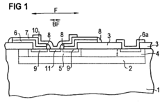
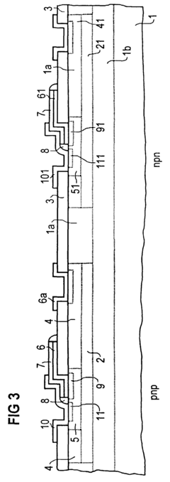
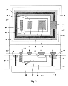
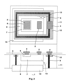
Vertical pnp transistor
PatentInactiveEP0855747A1
Innovation
- A vertical pnp transistor is produced with a self-aligned arrangement of emitter and base contacts using spacer insulation, where the emitter contact is formed from a p-doped polysilicon layer and the base contact is formed by outdiffusion into the substrate, allowing for simultaneous production with vertical npn transistors without significantly increasing process complexity.


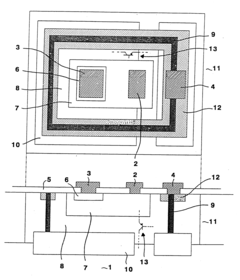
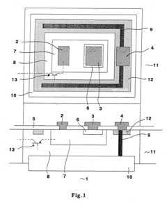
Transistor
PatentInactiveUS6734522B2
Innovation
- Incorporating a parasitic PNP transistor in the transistor structure, which operates during deep saturation to draw out excess minority carriers from the base and epitaxial region, thereby reducing the minority carrier lifetime and storage time.
Fabrication Techniques
The fabrication of PNP transistors involves several sophisticated techniques that have evolved over time to meet the demands of modern electronics. The process typically begins with the selection of a suitable semiconductor substrate, usually silicon, which serves as the foundation for the transistor structure.
One of the primary fabrication methods is epitaxial growth, where a thin layer of semiconductor material is deposited onto the substrate. This layer is carefully controlled to achieve the desired doping profile for the collector region of the PNP transistor. The epitaxial process allows for precise control over the thickness and composition of the semiconductor layers, which is crucial for optimizing transistor performance.
Following the epitaxial growth, photolithography techniques are employed to define the specific regions of the transistor. This process involves coating the wafer with a light-sensitive material called photoresist, exposing it to ultraviolet light through a mask, and then developing the pattern. The resulting pattern serves as a template for subsequent processing steps.
Ion implantation is another critical technique used in PNP transistor fabrication. This method allows for precise control over the doping of specific regions within the semiconductor. For a PNP transistor, boron ions are typically implanted to create the p-type emitter and collector regions, while phosphorus or arsenic ions may be used for the n-type base region.
Thermal diffusion is often used in conjunction with ion implantation to further distribute the dopants and activate them within the crystal lattice. This process involves heating the wafer to high temperatures, allowing the implanted ions to diffuse into the surrounding semiconductor material and occupy substitutional lattice sites.
Oxidation and etching processes play crucial roles in defining the transistor structure. Thermal oxidation is used to grow insulating layers of silicon dioxide, which serve as masks for subsequent etching steps or as part of the device's insulation. Various etching techniques, including wet chemical etching and plasma etching, are employed to selectively remove material and create the desired transistor geometry.
Metallization is the final major step in PNP transistor fabrication. This involves depositing metal layers to form the electrical contacts for the emitter, base, and collector regions. Typically, aluminum or copper is used, and the process may include multiple metal layers separated by insulating dielectrics to create complex interconnect structures.
Advanced packaging techniques are then applied to protect the fabricated transistors and integrate them into larger electronic systems. These may include wire bonding, flip-chip bonding, or more advanced 3D integration methods, depending on the specific application requirements.
Throughout the fabrication process, stringent quality control measures are implemented to ensure consistency and reliability. This includes in-line monitoring, parametric testing, and final electrical characterization of the completed PNP transistors.
Performance Metrics
Performance metrics are crucial for evaluating the effectiveness and efficiency of PNP transistors in various applications. These metrics provide quantitative measures of transistor behavior and capabilities, enabling engineers to select the most suitable components for specific circuit designs.
One of the primary performance metrics for PNP transistors is current gain, also known as beta (β) or hFE. This parameter represents the ratio of collector current to base current and indicates the transistor's amplification capability. Typical values for current gain in PNP transistors range from 20 to 300, with higher values indicating better amplification performance.
Another essential metric is the cutoff frequency (fT), which defines the highest frequency at which the transistor can effectively amplify signals. This parameter is particularly important in high-frequency applications, such as radio frequency (RF) circuits. PNP transistors generally have lower cutoff frequencies compared to their NPN counterparts, with typical values ranging from a few MHz to several hundred MHz.
Power dissipation is a critical performance metric that determines the maximum amount of power a transistor can handle without damage. This parameter is influenced by factors such as junction temperature, ambient temperature, and thermal resistance. PNP transistors typically have power dissipation ratings ranging from a few milliwatts to several watts, depending on their size and packaging.
Switching speed is another crucial metric, particularly in digital applications. It is characterized by parameters such as rise time, fall time, and propagation delay. PNP transistors generally exhibit slower switching speeds compared to NPN transistors due to the slower mobility of holes as charge carriers. Typical switching times for PNP transistors range from nanoseconds to microseconds, depending on the specific device and operating conditions.
Noise figure is an important performance metric for transistors used in low-noise amplifier applications. It quantifies the amount of noise added by the transistor to the input signal. PNP transistors typically have higher noise figures compared to NPN transistors, with values ranging from 1 to 10 dB, depending on the frequency and operating conditions.
Breakdown voltage is a critical parameter that defines the maximum voltage a transistor can withstand before entering avalanche breakdown. This metric is essential for determining the safe operating range of the transistor in high-voltage applications. PNP transistors are available with breakdown voltages ranging from a few volts to several hundred volts, depending on their design and intended use.
Finally, leakage current is an important performance metric that measures the small current flowing through the transistor when it is supposed to be in the off state. Lower leakage currents are desirable for improved efficiency and reduced power consumption. PNP transistors typically exhibit leakage currents in the range of nanoamperes to microamperes, depending on the device characteristics and operating temperature.
Unlock deeper insights with Patsnap Eureka Quick Research — get a full tech report to explore trends and direct your research. Try now!
Generate Your Research Report Instantly with AI Agent
Supercharge your innovation with Patsnap Eureka AI Agent Platform!