PNP Transistor Selection for RF Applications: Key Considerations
JUL 28, 20259 MIN READ
Generate Your Research Report Instantly with AI Agent
Patsnap Eureka helps you evaluate technical feasibility & market potential.
RF PNP Transistor Background and Objectives
PNP transistors have played a crucial role in radio frequency (RF) applications since their inception in the 1950s. These devices, characterized by their ability to amplify and switch high-frequency signals, have undergone significant evolution over the decades. The development of PNP transistors for RF applications has been driven by the ever-increasing demand for higher frequency operation, improved power efficiency, and enhanced linearity in wireless communication systems.
The primary objective in selecting PNP transistors for RF applications is to optimize performance across a range of critical parameters. These include high-frequency response, noise figure, power gain, linearity, and thermal stability. As the RF spectrum becomes increasingly crowded and new wireless technologies emerge, the need for PNP transistors capable of operating at higher frequencies while maintaining excellent signal integrity has become paramount.
Historically, the use of PNP transistors in RF circuits was limited due to their inherently slower switching speeds compared to NPN transistors. However, advancements in semiconductor manufacturing processes, particularly in silicon-germanium (SiGe) and III-V compound semiconductors, have significantly improved the high-frequency capabilities of PNP devices. This has expanded their applicability in RF front-end modules, mixers, and power amplifiers.
The evolution of RF PNP transistors has been closely tied to the progression of wireless communication standards. From early analog cellular systems to today's 5G networks, each generation has demanded transistors with improved performance characteristics. This has led to a continuous push for innovations in device structure, material composition, and fabrication techniques.
Key technological milestones in RF PNP transistor development include the introduction of heterojunction bipolar transistors (HBTs), which offer superior high-frequency performance and noise characteristics compared to conventional bipolar junction transistors (BJTs). Additionally, the development of advanced packaging techniques, such as flip-chip and wafer-level packaging, has enabled better integration of RF PNP transistors into compact, high-performance modules.
Looking ahead, the objectives for RF PNP transistor selection are focused on meeting the challenges posed by emerging wireless technologies, including 6G and beyond. These future systems will require transistors capable of operating at millimeter-wave and terahertz frequencies while maintaining high linearity and power efficiency. Furthermore, there is a growing emphasis on developing RF PNP transistors that can support multi-band operation and dynamic spectrum access, enabling more flexible and efficient use of the RF spectrum.
Market Analysis for RF PNP Transistors
The RF PNP transistor market has experienced steady growth in recent years, driven by the increasing demand for high-frequency applications in various industries. The global market for RF PNP transistors is expected to continue its upward trajectory, with a compound annual growth rate (CAGR) projected to be in the mid-single digits over the next five years.
The primary drivers of this market growth include the rapid expansion of 5G networks, the proliferation of Internet of Things (IoT) devices, and the growing adoption of wireless technologies in automotive and industrial sectors. As these industries continue to evolve, the need for high-performance RF components, including PNP transistors, is becoming increasingly critical.
In the telecommunications sector, the ongoing rollout of 5G infrastructure is creating a significant demand for RF PNP transistors. These components are essential for the development of base stations, small cells, and other network equipment that require efficient high-frequency signal processing. The automotive industry is another key market, with the integration of advanced driver assistance systems (ADAS) and in-vehicle connectivity solutions driving the need for robust RF components.
The consumer electronics segment remains a substantial market for RF PNP transistors, with smartphones, tablets, and wearable devices incorporating increasingly sophisticated RF front-end modules. Additionally, the industrial IoT sector is emerging as a promising market, as factories and manufacturing facilities adopt wireless sensor networks and smart monitoring systems.
Geographically, Asia-Pacific dominates the RF PNP transistor market, accounting for the largest share of global revenue. This is primarily due to the strong presence of semiconductor manufacturing facilities and the rapid adoption of new technologies in countries like China, South Korea, and Taiwan. North America and Europe follow as significant markets, driven by their advanced telecommunications infrastructure and robust automotive and aerospace industries.
The competitive landscape of the RF PNP transistor market is characterized by a mix of large multinational corporations and specialized semiconductor manufacturers. Key players in this space are continuously investing in research and development to improve transistor performance, reduce power consumption, and enhance integration capabilities. These efforts are crucial in meeting the evolving requirements of 5G, IoT, and other emerging applications.
Despite the positive growth outlook, the RF PNP transistor market faces challenges such as price pressure, supply chain disruptions, and the need for continuous innovation to keep pace with rapidly changing technology standards. Manufacturers are addressing these challenges through strategic partnerships, vertical integration, and the development of advanced packaging technologies.
Current Challenges in RF PNP Transistor Technology
The field of RF PNP transistor technology faces several significant challenges that hinder its widespread adoption and optimal performance in high-frequency applications. One of the primary issues is the inherent speed limitations of PNP transistors compared to their NPN counterparts. This speed discrepancy is due to the slower mobility of holes, which are the majority carriers in PNP devices, compared to electrons in NPN transistors.
Another critical challenge is the difficulty in achieving high current gain (β) at radio frequencies. As the frequency increases, the current gain of PNP transistors tends to roll off more rapidly than in NPN devices, limiting their effectiveness in RF amplification stages. This phenomenon is particularly problematic in applications requiring high linearity and low distortion.
Thermal management presents a significant hurdle in RF PNP transistor design. The higher resistance of P-type material leads to increased power dissipation, making it challenging to maintain stable operation at high frequencies and power levels. This thermal issue can result in performance degradation and reduced reliability in RF circuits.
Parasitic capacitances pose another substantial challenge in RF PNP transistor technology. The base-collector capacitance, in particular, can significantly impact high-frequency performance by creating unwanted feedback and limiting the maximum usable frequency of the device. Minimizing these parasitic effects while maintaining other desirable characteristics is a delicate balancing act for designers.
The manufacturing process for high-performance RF PNP transistors is also more complex and costly compared to NPN devices. Achieving the necessary doping profiles and junction characteristics for optimal RF performance requires precise control over fabrication parameters, which can lead to lower yields and higher production costs.
Noise figure optimization remains a persistent challenge in RF PNP transistor design. The inherent noise characteristics of PNP devices are generally inferior to those of NPN transistors, making it difficult to achieve the low noise figures required in sensitive RF front-end applications, such as low-noise amplifiers for receivers.
Lastly, the limited availability of comprehensive modeling and simulation tools specifically tailored for RF PNP transistors hinders accurate prediction of device behavior in complex RF circuits. This gap in design resources can lead to longer development cycles and increased reliance on empirical testing, which is both time-consuming and costly.
Existing RF PNP Transistor Selection Criteria
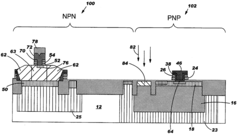
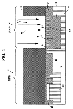
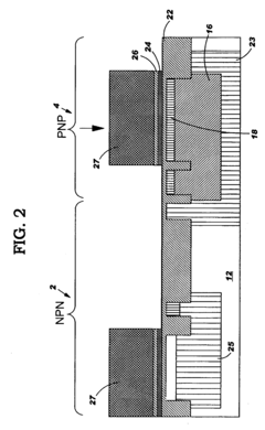
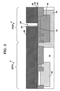
01 Structure and fabrication of PNP transistors
PNP transistors are semiconductor devices with specific structures and fabrication methods. They typically consist of a p-type emitter, n-type base, and p-type collector. The manufacturing process involves various steps such as doping, etching, and layering to create the desired transistor characteristics.- Structure and fabrication of PNP transistors: PNP transistors are semiconductor devices with specific structural designs and fabrication processes. These include methods for creating the emitter, base, and collector regions, as well as techniques for optimizing the device's performance through doping profiles and layer thicknesses.
- Applications of PNP transistors in integrated circuits: PNP transistors are widely used in various integrated circuit designs, including amplifiers, switches, and logic gates. They play crucial roles in analog and digital circuits, often complementing NPN transistors to create complementary designs for improved performance and power efficiency.
- PNP transistor characteristics and performance optimization: Improving the characteristics and performance of PNP transistors involves optimizing parameters such as current gain, frequency response, and noise characteristics. This includes techniques for reducing parasitic capacitances, improving thermal stability, and enhancing switching speeds.
- PNP transistors in power applications: PNP transistors are used in power applications, including voltage regulators, power supplies, and motor drivers. Designs focus on improving power handling capabilities, reducing power dissipation, and enhancing thermal management for high-current applications.
- Integration of PNP transistors with other semiconductor devices: PNP transistors are often integrated with other semiconductor devices to create complex circuits and systems. This includes their incorporation in BiCMOS processes, which combine bipolar and CMOS technologies, as well as their use in specialized analog and mixed-signal circuits.
02 Applications of PNP transistors in electronic circuits
PNP transistors are widely used in various electronic circuits for amplification, switching, and signal processing. They are often employed in complementary circuits with NPN transistors, power supplies, and analog circuits. Their unique characteristics make them suitable for specific applications in electronic design.Expand Specific Solutions03 Performance optimization of PNP transistors
Improving the performance of PNP transistors involves various techniques such as optimizing doping profiles, reducing parasitic capacitances, and enhancing current gain. These optimizations aim to improve switching speed, reduce power consumption, and increase overall efficiency of the transistor in electronic circuits.Expand Specific Solutions04 Integration of PNP transistors in semiconductor devices
PNP transistors are often integrated with other semiconductor components to create complex integrated circuits. This integration involves careful design considerations to ensure compatibility with other components, minimize interference, and optimize overall device performance. Various techniques are employed to achieve efficient integration in modern semiconductor devices.Expand Specific Solutions05 Testing and characterization of PNP transistors
Accurate testing and characterization of PNP transistors are crucial for quality control and performance evaluation. Various methods and equipment are used to measure parameters such as current gain, breakdown voltage, and leakage current. These tests ensure the reliability and consistency of PNP transistors in electronic applications.Expand Specific Solutions
Major RF PNP Transistor Manufacturers
The PNP transistor selection for RF applications market is in a mature stage, with established players and well-defined technologies. The global market size for RF transistors is estimated to be in the billions of dollars, driven by increasing demand in wireless communications, automotive, and consumer electronics sectors. Technologically, the field is advanced, with major companies like Infineon Technologies, NXP Semiconductors, and STMicroelectronics leading innovation. These firms, along with others such as Texas Instruments and Analog Devices, have developed high-performance PNP transistors optimized for RF applications, focusing on improved frequency response, low noise, and power efficiency. The competitive landscape is characterized by continuous R&D efforts to enhance transistor performance and meet evolving industry requirements.
Infineon Technologies AG
Technical Solution: Infineon has developed a range of PNP transistors optimized for RF applications, with a focus on power efficiency and linearity. Their BFP193W transistor, for instance, is designed for low-noise amplifiers and mixers in the 1-6 GHz range, offering a high fT of 8 GHz and a low noise figure of 0.8 dB at 1.8 GHz[3]. Infineon employs advanced SiGe:C (Silicon-Germanium with Carbon) technology in their RF transistors, which provides improved high-frequency characteristics and better temperature stability[4]. The company has also introduced innovative packaging solutions, such as TSFP (Thin Small Flat Package), to enhance RF performance and facilitate easier PCB integration.
Strengths: High linearity, excellent noise performance, advanced SiGe:C technology. Weaknesses: Potentially higher cost, may require specialized design considerations for optimal performance.
Texas Instruments Incorporated
Technical Solution: Texas Instruments (TI) has developed advanced PNP transistors for RF applications, focusing on high-frequency performance and low noise. Their BFT25A PNP transistor is designed for RF amplification up to 2 GHz, featuring a high transition frequency (fT) of 5 GHz and a low noise figure of 1.5 dB at 1 GHz[1]. TI's RF transistors incorporate SiGe technology, allowing for improved high-frequency response and reduced base resistance. The company has also implemented advanced packaging techniques, such as flip-chip technology, to minimize parasitic effects and improve thermal management in their RF transistors[2].
Strengths: High-frequency performance, low noise, advanced SiGe technology. Weaknesses: Potentially higher cost compared to standard silicon transistors, limited to specific frequency ranges.
Key Innovations in RF PNP Transistor Design
High performance vertical PNP transistor method
PatentInactiveUS20040248352A1
Innovation
- A method for fabricating high-performance vertical PNP transistors by incorporating an emitter region with silicon and germanium, sharing a single layer of silicon with the NPN transistor's base, and adding two additional masking steps to conventional CMOS and bipolar device fabrication processes, involving a SiGe low-temperature epitaxial layer and specific implantations to form the extrinsic and intrinsic bases.
High performance vertical PNP transistor and method
PatentInactiveUS20040099895A1
Innovation
- A method for fabricating high-performance vertical PNP transistors by incorporating an emitter region with silicon and germanium, sharing a single layer of silicon with the NPN transistor's base, and adding two additional masking steps to conventional CMOS and bipolar device fabrication processes, involving specific implantations and epitaxial layer growth to enhance PNP device performance.
RF PNP Transistor Performance Metrics
When selecting PNP transistors for RF applications, several key performance metrics must be considered to ensure optimal circuit operation. These metrics directly impact the transistor's ability to handle high-frequency signals and determine its suitability for specific RF applications.
One of the primary considerations is the transistor's transition frequency (fT), which represents the frequency at which the current gain drops to unity. A higher fT indicates better high-frequency performance, allowing the transistor to operate effectively at higher frequencies. For RF applications, transistors with fT values in the gigahertz range are typically preferred.
Another critical parameter is the maximum oscillation frequency (fmax), which defines the highest frequency at which the transistor can provide power gain. The fmax is often higher than fT and is particularly important for power amplifier designs. RF PNP transistors with higher fmax values offer superior performance in high-frequency oscillator and amplifier circuits.
Noise figure (NF) is a crucial metric for RF applications, especially in low-noise amplifiers (LNAs). It quantifies the amount of noise added by the transistor to the signal being amplified. Lower NF values are desirable, as they indicate better signal-to-noise ratio preservation. RF PNP transistors with low NF are essential for maintaining signal integrity in sensitive RF receiver circuits.
Power gain is another vital performance metric, particularly for RF power amplifiers. It measures the transistor's ability to amplify the input signal power. The power gain is often expressed in decibels (dB) and varies with frequency. RF PNP transistors with higher power gain at the desired operating frequency are preferred for efficient amplification.
Linearity is a critical factor in RF applications, as it affects the transistor's ability to accurately reproduce the input signal without distortion. Two important linearity metrics are the third-order intercept point (IP3) and the 1-dB compression point (P1dB). Higher IP3 and P1dB values indicate better linearity performance, which is crucial for maintaining signal fidelity in RF systems.
Input and output impedance matching are also essential considerations. RF PNP transistors should have well-defined input and output impedances that can be easily matched to the surrounding circuitry. This ensures efficient power transfer and minimizes signal reflections, which can degrade overall system performance.
Lastly, thermal characteristics and power handling capabilities are important for RF applications that involve high power levels. The maximum collector current (IC max) and power dissipation ratings determine the transistor's ability to handle high-power RF signals without degradation or failure. Proper thermal management and selection of transistors with adequate power ratings are crucial for reliable RF circuit operation.
Environmental Impact of RF PNP Transistors
The environmental impact of RF PNP transistors is an increasingly important consideration in the electronics industry. These devices, while essential for many radio frequency applications, can have significant ecological implications throughout their lifecycle.
Manufacturing processes for RF PNP transistors often involve the use of rare earth elements and potentially hazardous materials. The extraction and processing of these resources can lead to environmental degradation, including soil erosion, water pollution, and habitat destruction. Additionally, the production of these transistors requires substantial energy inputs, contributing to greenhouse gas emissions and climate change.
During their operational lifetime, RF PNP transistors consume energy and generate heat. While individual transistors have relatively low power requirements, the cumulative effect of millions of devices in use globally can be substantial. This energy consumption contributes to the overall carbon footprint of electronic systems and devices.
Electromagnetic radiation emitted by RF circuits utilizing PNP transistors is another environmental concern. While regulated within safe limits for human exposure, the long-term effects of increased electromagnetic fields on wildlife and ecosystems are not fully understood and require ongoing research.
The disposal and end-of-life management of RF PNP transistors present significant environmental challenges. These components often contain materials that are difficult to recycle or dispose of safely. Improper disposal can lead to the leaching of toxic substances into soil and water systems, posing risks to both human health and the environment.
However, advancements in transistor technology are addressing some of these environmental concerns. More efficient manufacturing processes are reducing energy consumption and waste. The development of more power-efficient RF PNP transistors is helping to minimize energy use during operation. Additionally, efforts to design transistors with more easily recyclable materials are gaining traction in the industry.
The electronics industry is also increasingly adopting circular economy principles, focusing on the reuse and recycling of components. This approach aims to reduce the environmental impact of RF PNP transistors by extending their useful life and improving end-of-life management.
Regulatory bodies worldwide are implementing stricter environmental standards for electronic components, including RF PNP transistors. These regulations are driving innovation in eco-friendly design and manufacturing processes, as well as encouraging more responsible disposal practices.
In conclusion, while RF PNP transistors play a crucial role in modern electronics, their environmental impact cannot be overlooked. Balancing technological advancement with environmental stewardship remains a key challenge for the industry. Continued research and innovation in sustainable materials, energy-efficient designs, and responsible manufacturing and disposal practices are essential for mitigating the environmental footprint of these critical components.
Unlock deeper insights with Patsnap Eureka Quick Research — get a full tech report to explore trends and direct your research. Try now!
Generate Your Research Report Instantly with AI Agent
Supercharge your innovation with Patsnap Eureka AI Agent Platform!