PNP Transistors: Strategies for Integration in Low-Power Modules
JUL 28, 20259 MIN READ
Generate Your Research Report Instantly with AI Agent
Patsnap Eureka helps you evaluate technical feasibility & market potential.
PNP Transistor Evolution and Integration Goals
PNP transistors have played a crucial role in the evolution of semiconductor technology since their inception in the mid-20th century. Initially developed as a complement to NPN transistors, PNP devices have undergone significant advancements to meet the growing demands of low-power applications. The primary goal in PNP transistor integration has been to enhance performance while reducing power consumption and minimizing device footprint.
The evolution of PNP transistors can be traced through several key milestones. Early germanium-based PNP transistors gave way to silicon-based devices, offering improved stability and reliability. The introduction of planar technology in the 1960s marked a significant leap, enabling more efficient manufacturing processes and better integration with other semiconductor components.
As the industry moved towards miniaturization, the development of bipolar junction transistors (BJTs) and their integration into integrated circuits (ICs) became a focal point. This shift necessitated innovations in PNP transistor design to address challenges such as current gain, frequency response, and thermal management within increasingly compact packages.
The emergence of complementary bipolar technology in the 1980s and 1990s further propelled PNP transistor development. This approach allowed for the creation of circuits that utilized both NPN and PNP transistors on the same substrate, leading to improved performance and reduced power consumption in analog and mixed-signal applications.
In recent years, the integration goals for PNP transistors have centered around their incorporation into low-power modules. This focus has driven research into novel materials, device structures, and fabrication techniques. Silicon-germanium (SiGe) heterojunction bipolar transistors (HBTs) have emerged as a promising technology, offering superior high-frequency performance and lower power consumption compared to traditional silicon BJTs.
The ongoing pursuit of Moore's Law has also influenced PNP transistor evolution, with efforts directed towards scaling devices to nanometer dimensions while maintaining or improving their electrical characteristics. This has led to the exploration of advanced process nodes and three-dimensional integration techniques to maximize device density and minimize parasitic effects.
Looking ahead, the integration goals for PNP transistors in low-power modules are multifaceted. Researchers and engineers are striving to further reduce power consumption through innovative circuit designs and improved device physics. Additionally, there is a strong emphasis on enhancing the compatibility of PNP transistors with complementary metal-oxide-semiconductor (CMOS) technology, enabling seamless integration in mixed-signal systems.
Low-Power Module Market Analysis
The low-power module market has experienced significant growth in recent years, driven by the increasing demand for energy-efficient electronic devices across various industries. This market segment is particularly crucial for portable and battery-powered devices, where power consumption is a critical factor in determining product performance and user experience.
The global low-power module market is expected to continue its upward trajectory, with a compound annual growth rate (CAGR) projected to remain strong over the next five years. This growth is primarily fueled by the rapid adoption of Internet of Things (IoT) devices, wearable technology, and the ongoing miniaturization of electronic components.
Key industries driving the demand for low-power modules include consumer electronics, healthcare, automotive, and industrial automation. In the consumer electronics sector, smartphones, tablets, and smart home devices are major contributors to market growth. The healthcare industry is increasingly incorporating low-power modules in medical wearables and remote patient monitoring systems. The automotive sector is adopting these modules for advanced driver assistance systems (ADAS) and in-vehicle infotainment systems.
The integration of PNP transistors in low-power modules plays a crucial role in meeting the market's demands for improved energy efficiency and reduced power consumption. PNP transistors offer advantages in certain circuit configurations, particularly in applications requiring high-side switching or complementary push-pull output stages.
Market trends indicate a growing preference for integrated solutions that combine multiple functions within a single module. This integration trend is driving the development of more sophisticated low-power modules that incorporate PNP transistors alongside other components, such as NPN transistors, resistors, and capacitors.
Geographically, Asia-Pacific dominates the low-power module market, with China, Japan, and South Korea being major contributors. The region's strong presence in consumer electronics manufacturing and its rapidly growing IoT ecosystem are key factors driving this dominance. North America and Europe follow, with significant market shares driven by their advanced automotive and healthcare industries.
The competitive landscape of the low-power module market is characterized by a mix of established semiconductor companies and innovative startups. Key players are focusing on research and development to improve the performance and efficiency of their low-power modules, with a particular emphasis on integrating advanced transistor technologies, including optimized PNP designs.
As the demand for more energy-efficient and compact electronic devices continues to rise, the low-power module market is expected to present significant opportunities for growth and innovation. The successful integration of PNP transistors in these modules will be a critical factor in meeting the evolving needs of various industries and applications.
PNP Integration Challenges in Low-Power Designs
The integration of PNP transistors in low-power modules presents several significant challenges that designers must address to achieve optimal performance and efficiency. One of the primary obstacles is the inherent slower switching speed of PNP transistors compared to their NPN counterparts. This speed limitation can impact the overall performance of low-power circuits, particularly in applications requiring high-frequency operation or rapid response times.
Another critical challenge lies in the management of power consumption. PNP transistors typically exhibit higher power dissipation than NPN transistors, which can be problematic in low-power designs where energy efficiency is paramount. This increased power consumption is often attributed to the larger base current required for PNP transistors to achieve the same collector current as NPN devices.
The issue of thermal management also becomes more complex when integrating PNP transistors. The higher power dissipation can lead to localized heating, potentially affecting the performance and reliability of nearby components. This thermal challenge is exacerbated in compact low-power modules where space for heat dissipation is limited.
Furthermore, the voltage drop across PNP transistors tends to be greater than that of NPN transistors, which can reduce the available voltage swing in low-voltage applications. This characteristic can constrain circuit design options and potentially impact signal integrity in analog circuits.
The physical layout and fabrication process for PNP transistors also present integration challenges. PNP structures often require more silicon area than NPN transistors for equivalent performance, which can increase overall chip size and cost. Additionally, the process of optimizing PNP transistor characteristics while maintaining compatibility with existing CMOS processes can be complex and may require specialized fabrication techniques.
Noise performance is another area of concern when integrating PNP transistors in low-power designs. These devices can exhibit higher noise levels, particularly at low frequencies, which can be problematic in sensitive analog circuits or in applications requiring high signal-to-noise ratios.
Lastly, the availability and variety of PNP transistors suitable for low-power applications may be more limited compared to NPN options. This can restrict design flexibility and may require engineers to make compromises in performance or functionality to accommodate the available PNP devices.
Addressing these challenges requires a multifaceted approach, combining innovative circuit design techniques, advanced fabrication processes, and careful consideration of device characteristics to successfully integrate PNP transistors in low-power modules while meeting performance, efficiency, and reliability requirements.
Current PNP Integration Techniques
01 PNP transistor structure and fabrication
This category covers the basic structure and fabrication methods of PNP transistors. It includes the design of emitter, base, and collector regions, as well as the processes used to create these structures on semiconductor substrates. Various techniques for doping, etching, and layer deposition are discussed to achieve optimal PNP transistor performance.- PNP transistor structure and fabrication: This category covers the basic structure and fabrication methods of PNP transistors. It includes the design of emitter, base, and collector regions, as well as the techniques used to create these structures on semiconductor substrates. The fabrication process may involve epitaxial growth, ion implantation, and various etching techniques to achieve the desired transistor characteristics.
- PNP transistor applications in integrated circuits: PNP transistors are widely used in various integrated circuit designs. This category explores their applications in analog and digital circuits, including amplifiers, current mirrors, and logic gates. It also covers the integration of PNP transistors with other semiconductor devices to create complex circuit functions on a single chip.
- PNP transistor performance optimization: This category focuses on techniques to improve the performance of PNP transistors. It includes methods to enhance parameters such as current gain, frequency response, and power handling capabilities. Optimization strategies may involve adjusting doping profiles, modifying device geometry, or incorporating advanced materials to achieve better transistor characteristics.
- PNP transistors in power electronics: PNP transistors play a crucial role in power electronics applications. This category covers their use in high-power circuits, switching regulators, and motor control systems. It includes design considerations for handling high voltages and currents, as well as thermal management techniques to ensure reliable operation in power-intensive environments.
- PNP transistor modeling and simulation: This category deals with the development of accurate models for PNP transistors and their implementation in circuit simulation tools. It covers various modeling approaches, including physics-based models and empirical models, to predict transistor behavior under different operating conditions. These models are essential for designing and optimizing circuits that incorporate PNP transistors.
02 PNP transistor applications in integrated circuits
PNP transistors are widely used in integrated circuits for various applications. This category explores their implementation in analog and digital circuits, including amplifiers, current mirrors, and logic gates. It also covers the integration of PNP transistors with other semiconductor devices to create complex circuit functions.Expand Specific Solutions03 PNP transistor performance optimization
This category focuses on techniques to improve PNP transistor performance. It includes methods for reducing parasitic capacitances, minimizing base resistance, and enhancing current gain. Advanced designs such as vertical and lateral PNP structures are explored to achieve better frequency response and power handling capabilities.Expand Specific Solutions04 PNP transistors in power electronics
PNP transistors play a crucial role in power electronics applications. This category covers their use in high-voltage and high-current circuits, including power supplies, motor drivers, and voltage regulators. It also discusses techniques for improving thermal management and breakdown voltage in power PNP transistors.Expand Specific Solutions05 PNP transistors in analog and mixed-signal circuits
This category explores the use of PNP transistors in analog and mixed-signal circuit designs. It covers their implementation in operational amplifiers, comparators, and data converters. The focus is on leveraging PNP transistor characteristics to achieve better linearity, noise performance, and temperature stability in these circuits.Expand Specific Solutions
Key Players in PNP Transistor Manufacturing
The integration of PNP transistors in low-power modules is currently in a mature development stage, with a competitive landscape shaped by established semiconductor manufacturers and research institutions. The market for these components is substantial, driven by the growing demand for energy-efficient electronics across various industries. Companies like Texas Instruments, Infineon Technologies, and STMicroelectronics are at the forefront, leveraging their extensive experience in semiconductor design and manufacturing to develop advanced PNP transistor solutions. Research institutions such as Fudan University and IHP GmbH are contributing to technological advancements, while emerging players like GlobalFoundries and SK hynix are also making significant strides in this field. The technology's maturity is evident in the widespread adoption of PNP transistors in low-power applications, with ongoing research focused on further miniaturization and efficiency improvements.
International Business Machines Corp.
Technical Solution: IBM has developed advanced PNP transistor integration strategies for low-power modules, focusing on silicon-on-insulator (SOI) technology. Their approach involves using ultra-thin body and buried oxide (UTBB) SOI structures to enhance PNP transistor performance while reducing power consumption. IBM's technique includes optimizing the base-emitter junction profile and implementing advanced doping methods to minimize parasitic capacitances[1]. They have also introduced a novel vertical PNP structure with a self-aligned emitter-base junction, which significantly improves the current gain and frequency response of the transistor[3]. Additionally, IBM has developed a complementary bipolar process that allows for the integration of high-performance PNP transistors alongside NPN devices on the same chip, enabling more efficient and compact low-power module designs[5].
Strengths: Superior PNP performance in SOI technology, reduced power consumption, and improved integration density. Weaknesses: Potentially higher manufacturing costs and complexity compared to traditional bulk CMOS processes.
Texas Instruments Incorporated
Technical Solution: Texas Instruments has pioneered innovative strategies for integrating PNP transistors in low-power modules, focusing on their BiCOM technology. Their approach combines bipolar and CMOS processes to create high-performance, low-power analog and mixed-signal circuits. TI's PNP integration strategy involves using a vertical PNP structure with optimized collector, base, and emitter regions to achieve high current gain and low parasitic capacitances[2]. They have also developed a unique shallow trench isolation (STI) technique that reduces collector-substrate capacitance, improving the transistor's frequency response[4]. Furthermore, TI has implemented advanced epitaxial growth methods to create ultra-thin, highly doped base regions, which enhance the PNP transistor's speed while maintaining low power consumption[6]. Their process also includes the integration of high-quality passive components, allowing for more compact and efficient low-power module designs.
Strengths: Excellent analog performance, low power consumption, and high integration capability. Weaknesses: May have limitations in very high-frequency applications compared to some specialized RF processes.
Innovative PNP Design Approaches
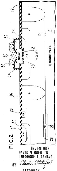
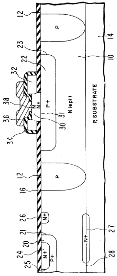
Integrated circuit with a high speed narrow base width vertical PNP transistor
PatentInactiveUS6809396B2
Innovation
- A semiconductor device is fabricated with both high-performance NPN and PNP vertical transistors on a monocrystalline silicon substrate, utilizing a heavily doped base layer, epitaxial layers, and buried layers to reduce parasitic capacitance and collector resistance, along with trench isolation and tailored doping profiles to achieve low manufacturing costs and high frequency response.
Complementary NPN/PNP structure for monolithic integrated circuits
PatentInactiveUS3611067A
Innovation
- A semiconductor substrate is divided into isolated areas with a double-diffused NPN transistor and a PNP transistor featuring a diffused emitter, an epitaxial base, and a Schottky-barrier collector-base junction, where the emitter of the PNP transistor is formed during the base diffusion of the NPN transistor, avoiding additional high-temperature processing steps and enabling a vertical structure for the PNP transistor with a frequency response of up to 50 MegaHertz.
Power Efficiency Optimization Strategies
Power efficiency optimization is a critical aspect of integrating PNP transistors into low-power modules. The primary goal is to minimize power consumption while maintaining or enhancing performance. One key strategy involves optimizing the transistor's operating point to reduce static power dissipation. This can be achieved through careful biasing techniques and the implementation of advanced circuit topologies that leverage the unique characteristics of PNP transistors.
Another important approach is the use of dynamic power management techniques. These methods involve selectively activating or deactivating portions of the circuit based on real-time performance requirements. By implementing intelligent power gating and clock gating mechanisms, designers can significantly reduce overall power consumption without compromising functionality.
The optimization of transistor sizing and layout also plays a crucial role in power efficiency. By carefully adjusting the dimensions of PNP transistors and optimizing their physical arrangement within the module, designers can minimize parasitic capacitances and resistances, leading to reduced power losses and improved switching speeds.
Advanced process technologies and materials can further enhance power efficiency. The use of silicon-on-insulator (SOI) substrates, for instance, can reduce parasitic capacitances and leakage currents, resulting in lower power consumption. Similarly, the incorporation of high-k dielectrics and metal gates can improve the transistor's electrostatic control, allowing for lower operating voltages and reduced power dissipation.
Thermal management strategies are equally important in optimizing power efficiency. Effective heat dissipation techniques, such as the use of advanced packaging materials and innovative cooling solutions, can help maintain optimal operating temperatures for PNP transistors, thereby reducing temperature-dependent leakage currents and improving overall efficiency.
The implementation of adaptive voltage scaling (AVS) and dynamic frequency scaling (DFS) techniques can further optimize power consumption. These methods allow for real-time adjustment of supply voltages and operating frequencies based on workload requirements, ensuring that the PNP transistors operate at the minimum necessary power levels while still meeting performance targets.
Lastly, the integration of power-aware design methodologies throughout the development process is essential. This includes the use of advanced simulation and modeling tools to accurately predict power consumption at various stages of design, as well as the implementation of power-optimized synthesis and place-and-route algorithms during the physical implementation phase.
Thermal Management Considerations
Thermal management is a critical consideration in the integration of PNP transistors into low-power modules. As these devices operate, they generate heat that must be effectively dissipated to maintain optimal performance and reliability. The compact nature of low-power modules presents unique challenges in managing thermal issues, requiring innovative approaches to heat dissipation.
One of the primary concerns in thermal management for PNP transistors is the impact of temperature on device characteristics. As temperature increases, parameters such as current gain, leakage current, and switching speed can be significantly affected. This can lead to reduced efficiency and potential reliability issues in the overall module. To address this, designers must carefully consider the thermal resistance of the transistor package and its interface with the surrounding components.
Heat spreading techniques play a crucial role in managing the thermal profile of PNP transistors in low-power modules. The use of thermally conductive materials, such as copper or aluminum, in the substrate or package design can help distribute heat more evenly across the module. This approach reduces hot spots and minimizes the risk of localized thermal stress on the transistors.
Advanced packaging technologies, such as flip-chip bonding or the use of thermal vias, can significantly improve heat dissipation from PNP transistors. These techniques provide more direct thermal paths from the transistor junction to the external environment, reducing overall thermal resistance. In some cases, the integration of miniature heat sinks or heat spreaders directly onto the transistor package can further enhance thermal performance.
The layout and placement of PNP transistors within the low-power module also play a critical role in thermal management. Strategic positioning of these devices, taking into account the thermal characteristics of neighboring components, can help optimize heat distribution across the module. This may involve creating thermal zones or implementing thermal isolation techniques to prevent heat from sensitive components from affecting the PNP transistors' performance.
Active cooling solutions, while less common in low-power modules, may be considered for applications with particularly stringent thermal requirements. Miniature fans or thermoelectric coolers could be integrated to provide localized cooling for PNP transistors in high-performance, low-power designs. However, the power consumption and space requirements of these active cooling solutions must be carefully balanced against the overall module design goals.
Thermal simulation and modeling tools are invaluable in optimizing the thermal management of PNP transistors in low-power modules. These tools allow designers to predict and analyze heat distribution, identify potential thermal bottlenecks, and evaluate the effectiveness of various cooling strategies before physical prototyping. This approach can significantly reduce development time and costs while ensuring optimal thermal performance in the final product.
Unlock deeper insights with Patsnap Eureka Quick Research — get a full tech report to explore trends and direct your research. Try now!
Generate Your Research Report Instantly with AI Agent
Supercharge your innovation with Patsnap Eureka AI Agent Platform!