

Reference Designs And BOM For UCIe Chiplet Interconnect
SEP 1, 20259 MIN READ
Generate Your Research Report Instantly with AI Agent
PatSnap Eureka helps you evaluate technical feasibility & market potential.
UCIe Chiplet Technology Background and Objectives
Universal Chiplet Interconnect Express (UCIe) represents a significant advancement in semiconductor integration technology, emerging as a response to the increasing challenges of traditional monolithic chip scaling. The evolution of semiconductor technology has historically followed Moore's Law, with transistor density doubling approximately every two years. However, as process nodes have shrunk below 5nm, physical limitations and exponentially rising manufacturing costs have necessitated alternative approaches to continue performance scaling.
Chiplet technology, the foundation of UCIe, addresses these challenges by disaggregating traditional monolithic designs into smaller, specialized silicon dies (chiplets) that can be manufactured using optimal process nodes for each function and then integrated into a single package. This approach enables continued performance scaling while managing costs and manufacturing complexity.
UCIe specifically emerged in 2022 as an open industry standard for chiplet interconnection, backed by major industry players including Intel, AMD, Arm, TSMC, Samsung, and Google. The standard aims to establish a universal die-to-die interconnect that enables chiplets from different vendors to work seamlessly together, fostering an open chiplet ecosystem.
The technical objectives of UCIe focus on providing high-bandwidth, low-latency, and energy-efficient communication between chiplets within a package. The standard defines both physical layer specifications and protocol stack implementations, supporting data rates from 16 GT/s to 32 GT/s per pin in its first iteration, with a roadmap for future enhancements.
UCIe addresses several critical technical goals: standardizing die-to-die interfaces to enable multi-vendor interoperability, optimizing power efficiency for inter-chiplet communication, establishing packaging requirements for reliable connections, and defining testing methodologies to ensure quality and performance.
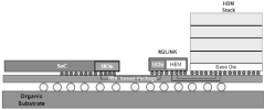
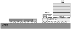
The standard encompasses two primary packaging technologies: standard packages with organic substrates and advanced packaging using silicon interposers. This flexibility allows manufacturers to choose appropriate integration methods based on performance requirements and cost considerations.
Reference designs and bill of materials (BOM) for UCIe implementations represent crucial resources for semiconductor companies looking to adopt this technology. These reference materials provide validated circuit designs, component specifications, and implementation guidelines that reduce development risks and accelerate time-to-market for UCIe-compliant products.
As the industry continues to face scaling challenges, UCIe technology aims to democratize chiplet-based design by enabling a modular approach to system-on-chip development, potentially reshaping the semiconductor industry's innovation model from vertical integration toward more collaborative and specialized development ecosystems.
Chiplet technology, the foundation of UCIe, addresses these challenges by disaggregating traditional monolithic designs into smaller, specialized silicon dies (chiplets) that can be manufactured using optimal process nodes for each function and then integrated into a single package. This approach enables continued performance scaling while managing costs and manufacturing complexity.
UCIe specifically emerged in 2022 as an open industry standard for chiplet interconnection, backed by major industry players including Intel, AMD, Arm, TSMC, Samsung, and Google. The standard aims to establish a universal die-to-die interconnect that enables chiplets from different vendors to work seamlessly together, fostering an open chiplet ecosystem.
The technical objectives of UCIe focus on providing high-bandwidth, low-latency, and energy-efficient communication between chiplets within a package. The standard defines both physical layer specifications and protocol stack implementations, supporting data rates from 16 GT/s to 32 GT/s per pin in its first iteration, with a roadmap for future enhancements.
UCIe addresses several critical technical goals: standardizing die-to-die interfaces to enable multi-vendor interoperability, optimizing power efficiency for inter-chiplet communication, establishing packaging requirements for reliable connections, and defining testing methodologies to ensure quality and performance.
The standard encompasses two primary packaging technologies: standard packages with organic substrates and advanced packaging using silicon interposers. This flexibility allows manufacturers to choose appropriate integration methods based on performance requirements and cost considerations.
Reference designs and bill of materials (BOM) for UCIe implementations represent crucial resources for semiconductor companies looking to adopt this technology. These reference materials provide validated circuit designs, component specifications, and implementation guidelines that reduce development risks and accelerate time-to-market for UCIe-compliant products.
As the industry continues to face scaling challenges, UCIe technology aims to democratize chiplet-based design by enabling a modular approach to system-on-chip development, potentially reshaping the semiconductor industry's innovation model from vertical integration toward more collaborative and specialized development ecosystems.
Market Demand Analysis for Chiplet-Based Solutions
The chiplet-based semiconductor market is experiencing unprecedented growth, driven by the increasing demand for high-performance computing solutions across various industries. Current market analyses indicate that the global chiplet market is projected to grow at a compound annual growth rate of 40% from 2023 to 2030, reaching significant market valuation by the end of the forecast period. This remarkable growth trajectory is primarily fueled by the escalating need for advanced computing capabilities in data centers, artificial intelligence applications, and high-performance computing environments.
The demand for UCIe (Universal Chiplet Interconnect Express) chiplet interconnect solutions is particularly strong in the data center segment, where the need for efficient, high-bandwidth, and low-latency communication between chiplets is critical. Enterprise customers are increasingly seeking modular chip designs that allow for more flexible and cost-effective scaling of computing resources, making chiplet-based architectures an attractive alternative to traditional monolithic designs.
Cloud service providers represent another significant market segment driving demand for chiplet solutions. These providers require scalable and energy-efficient computing platforms to support their rapidly expanding infrastructure. The ability to mix and match chiplets from different vendors and process nodes offers these providers greater flexibility in designing systems tailored to their specific workload requirements.
The artificial intelligence and machine learning sector is emerging as a key growth driver for chiplet-based solutions. As AI models continue to grow in size and complexity, the computational demands placed on hardware accelerators increase exponentially. Chiplet architectures enable the development of specialized AI processors that can deliver the necessary performance while maintaining reasonable power consumption and thermal characteristics.
Consumer electronics manufacturers are also showing interest in chiplet technology, particularly for high-end devices requiring substantial computing power. The ability to integrate heterogeneous components using chiplet architecture allows for more efficient use of silicon area and potentially lower manufacturing costs compared to monolithic designs.
From a geographical perspective, North America currently leads the market for chiplet-based solutions, followed by Asia-Pacific and Europe. However, the Asia-Pacific region is expected to witness the highest growth rate during the forecast period, driven by the presence of major semiconductor manufacturers and increasing investments in advanced semiconductor technologies.
The market demand for standardized reference designs and bill of materials (BOM) for UCIe chiplet interconnect is particularly strong, as these resources can significantly reduce development time and costs for companies looking to adopt chiplet-based architectures. Standardization efforts through the UCIe consortium are creating a more accessible ecosystem for chiplet integration, further accelerating market adoption across various industry segments.
UCIe Interconnect Technical Challenges and Standards
UCIe (Universal Chiplet Interconnect Express) represents a significant advancement in chiplet-based system design, addressing the growing need for high-performance, energy-efficient interconnects between chiplets. The standard faces several technical challenges that must be overcome to ensure widespread adoption and implementation.
One primary challenge is signal integrity across the die-to-die interface. As data rates increase to meet bandwidth demands, maintaining signal quality becomes increasingly difficult due to crosstalk, jitter, and impedance mismatches. The UCIe standard must address these issues while supporting data rates up to 32 GT/s in advanced implementations, requiring sophisticated equalization techniques and careful physical design considerations.
Power efficiency presents another significant hurdle. With computing systems increasingly constrained by power and thermal limitations, UCIe implementations must minimize energy consumption per bit transferred. This necessitates innovations in low-power circuit design, efficient clock distribution networks, and intelligent power management schemes that can adapt to varying workloads and communication patterns.
Physical integration challenges also exist, particularly regarding bump pitch and alignment tolerances. As chiplets become smaller and interconnect densities increase, manufacturing processes must achieve extremely precise alignment between dies. The standard must accommodate these manufacturing realities while still enabling high-yield, cost-effective production.
The UCIe standard addresses these challenges through a comprehensive specification that defines both physical and protocol layers. At the physical layer, it specifies electrical characteristics, signaling methods, and physical dimensions for die-to-die interfaces. The standard supports multiple packaging technologies, including both silicon interposer and organic substrate approaches, providing flexibility for different application requirements and cost targets.
At the protocol layer, UCIe defines transaction protocols that ensure reliable data transfer while supporting various traffic patterns common in modern computing systems. The standard incorporates advanced features such as flow control, error detection and correction, and quality of service mechanisms to ensure robust operation under diverse conditions.
Interoperability represents a cornerstone of the UCIe standard. By establishing clear compliance and testing methodologies, the standard enables chiplets from different vendors to work together seamlessly, fostering an ecosystem of specialized components that can be integrated into complex systems. This "mix-and-match" capability is crucial for the long-term success of chiplet-based design approaches.
The UCIe Consortium continues to evolve the standard to address emerging challenges and incorporate new technologies, ensuring that it remains relevant as computing requirements advance. Working groups focus on areas such as advanced packaging technologies, increased bandwidth capabilities, and enhanced security features to meet the demands of next-generation computing systems.
Current UCIe Reference Design Implementations
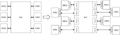
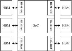
01 UCIe chiplet interconnect architecture and design
Universal Chiplet Interconnect Express (UCIe) architecture provides standardized die-to-die interconnect for chiplet-based designs. These reference designs include specifications for physical layer connections, protocols, and signal integrity considerations to ensure reliable high-speed communication between chiplets. The architecture supports various packaging technologies and enables modular chip design with improved performance and power efficiency.- UCIe chiplet interconnect architecture and design: The Universal Chiplet Interconnect Express (UCIe) architecture provides standardized die-to-die interconnects for chiplet-based designs. These reference designs include specifications for physical layer connections, protocols, and signal integrity considerations to ensure reliable high-speed communication between chiplets. The architecture supports various packaging technologies and enables modular chip design with improved performance and power efficiency.
- Thermal management solutions for UCIe implementations: Thermal management is critical in UCIe chiplet designs due to high power density and heat generation at interconnect points. Reference designs incorporate thermal interface materials, heat spreaders, and cooling solutions specifically optimized for multi-die packages. These solutions address hotspots at die interfaces and ensure reliable operation of high-bandwidth interconnects while maintaining signal integrity across temperature variations.
- Power delivery networks for UCIe chiplet systems: Power delivery networks for UCIe implementations require specialized designs to handle the unique requirements of chiplet-based systems. Reference designs include power distribution architectures that minimize voltage drops across interconnects, reduce power integrity issues, and support different power domains across multiple chiplets. These designs incorporate decoupling capacitor placement strategies and power grid optimizations to ensure stable operation of high-speed interfaces.
- Testing and validation methodologies for UCIe interconnects: Testing and validation methodologies for UCIe interconnects include specialized procedures for verifying signal integrity, interoperability, and compliance with the UCIe specification. Reference designs incorporate test structures, debug interfaces, and validation protocols to ensure proper functioning of die-to-die connections. These methodologies address challenges in testing high-speed interfaces across multiple chiplets and include recommendations for production testing and quality assurance.
- UCIe packaging technologies and materials: UCIe reference designs specify packaging technologies and bill of materials (BOM) for implementing chiplet-based systems. These include substrate materials, microbump specifications, underfill requirements, and assembly processes optimized for high-density interconnects. The packaging solutions address challenges in alignment precision, coefficient of thermal expansion matching, and reliability while supporting the high bandwidth and low latency requirements of UCIe interfaces.
02 Chiplet integration and packaging solutions
Integration and packaging solutions for UCIe chiplets involve advanced techniques for connecting multiple dies within a single package. These solutions address thermal management, power delivery, and mechanical stability challenges. Reference designs include specifications for interposer technologies, through-silicon vias (TSVs), and micro-bumps that facilitate high-density interconnections while maintaining signal integrity across chiplet boundaries.Expand Specific Solutions03 Power management and thermal solutions for UCIe implementations
Power management and thermal solutions are critical components of UCIe chiplet designs. Reference designs include specifications for power delivery networks, voltage regulation modules, and thermal interface materials. These solutions address the challenges of delivering stable power to multiple chiplets while managing heat dissipation to ensure reliable operation and prevent thermal throttling in high-performance computing applications.Expand Specific Solutions04 Testing and validation methodologies for UCIe chiplet designs
Testing and validation methodologies for UCIe chiplet designs include procedures for verifying electrical performance, signal integrity, and protocol compliance. Reference designs specify test points, measurement techniques, and acceptance criteria for validating chiplet interconnects. These methodologies ensure interoperability between chiplets from different vendors and help identify potential issues before final assembly, reducing development time and manufacturing costs.Expand Specific Solutions05 Bill of Materials (BOM) components for UCIe implementations
Bill of Materials components for UCIe implementations include specialized connectors, passive components, and supporting ICs required for chiplet-based designs. Reference designs specify recommended components such as high-speed connectors, decoupling capacitors, termination resistors, and clock generation circuits. These components are selected to meet the electrical requirements of the UCIe specification while optimizing for cost, availability, and reliability in volume production.Expand Specific Solutions
Key Industry Players in Chiplet Ecosystem
The UCIe chiplet interconnect technology is currently in an early growth phase, with market adoption accelerating as major semiconductor players recognize its potential to address scaling challenges. The global chiplet market is projected to expand significantly, driven by demands for heterogeneous integration and improved performance efficiency. From a technical maturity perspective, industry leaders including Intel, AMD (formerly Xilinx), TSMC, and Qualcomm are making substantial investments in UCIe reference designs and BOM standardization. While Intel has established early leadership through its foundational work on the UCIe standard, companies like Samsung, Apple, and Huawei are rapidly developing competitive solutions. The ecosystem is evolving from proprietary implementations toward standardized approaches, with semiconductor manufacturers and packaging specialists collaborating to address interoperability challenges.
Intel Corp.
Technical Solution: Intel is a founding member of the UCIe consortium and has been at the forefront of chiplet technology development. Their reference design for UCIe implementation focuses on a disaggregated approach using their EMIB (Embedded Multi-die Interconnect Bridge) and Foveros packaging technologies. Intel's UCIe reference design includes a comprehensive BOM featuring their P-Tile and E-Tile chiplets that support both die-to-die and package-to-package connections. The design incorporates advanced PHY layers operating at 16-32 GT/s with power efficiency of <1 pJ/bit. Intel has developed specialized UCIe adapters that bridge between different protocols and their reference implementation includes validation tools for signal integrity testing and compliance verification. Their UCIe solution supports both standard and advanced protocols with built-in security features for authenticated die-to-die communications.
Strengths: Industry-leading packaging technologies (EMIB and Foveros) that complement UCIe implementation; extensive ecosystem support; comprehensive validation tools. Weaknesses: Proprietary elements may limit interoperability with other vendors' chiplets; higher implementation costs compared to some competitors.
QUALCOMM, Inc.
Technical Solution: Qualcomm has developed UCIe reference designs specifically optimized for mobile and edge computing applications. Their implementation focuses on ultra-low power consumption while maintaining high bandwidth connections between heterogeneous chiplets. Qualcomm's UCIe BOM includes specialized PHY layers designed for <0.5 pJ/bit energy efficiency at 16 GT/s, making it particularly suitable for battery-powered devices. Their reference design incorporates adaptive power management that can dynamically adjust link speeds based on workload requirements. Qualcomm has also developed a modular approach to UCIe implementation that allows system designers to select specific components based on application needs. Their design includes specialized test fixtures and validation methodologies for ensuring compliance with the UCIe 1.0 specification while optimizing for mobile form factors and thermal constraints.
Strengths: Industry-leading power efficiency optimized for mobile applications; flexible implementation options; strong expertise in heterogeneous integration. Weaknesses: Less focus on high-performance computing applications; more limited ecosystem compared to Intel.
Critical IP and Technical Specifications for UCIe
Semiconductor device based on UCIe interface
PatentActiveCN117222234A
Innovation
- Using semiconductor devices based on the UCIe interface, the SoC is decoupled from the HBM through joint dies, and the rewiring layer and organic substrate are used for interconnection, avoiding the silicon interposer, realizing the decoupling of the SoC and HBM memory, and through the on-chip bus Perform data exchange.
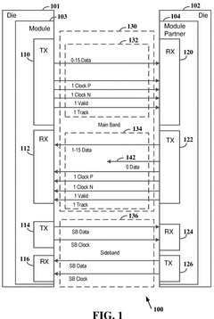
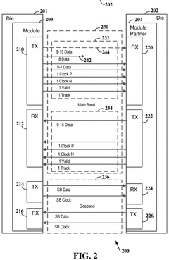
Variable link width in two directions for main band chip module connection
PatentWO2024226177A1
Innovation
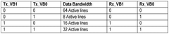
- Implementing a variable link width mechanism in both directions of the main band connection, allowing for dynamic adjustment of the number of active data lanes based on requirements through a sideband communication protocol, enabling independent configuration of transmit and receive data lines to optimize power usage and data rates.

Supply Chain Considerations for UCIe Components
The UCIe (Universal Chiplet Interconnect Express) ecosystem requires a robust and reliable supply chain to ensure successful implementation of chiplet-based designs. The supply chain for UCIe components presents unique challenges and opportunities that must be carefully considered by manufacturers and system integrators.
Component sourcing for UCIe implementations involves multiple specialized suppliers across the semiconductor industry. Key components include die-to-die PHY interfaces, package substrates with high-density routing capabilities, and advanced packaging materials. The relatively new nature of the UCIe standard means that supplier qualification processes must be particularly rigorous, with emphasis on manufacturing consistency and quality control.
Geographical distribution of UCIe component suppliers presents strategic considerations. Currently, advanced packaging capabilities are concentrated in East Asia, particularly Taiwan, Japan, and South Korea, while design expertise is more distributed globally. This geographic concentration creates potential supply chain vulnerabilities that organizations should address through diversification strategies and alternative sourcing plans.
Lead times for specialized UCIe components can significantly impact product development schedules. Advanced substrate materials and custom silicon interposers often require 16-24 weeks lead time under normal conditions, which can extend further during industry-wide capacity constraints. Organizations implementing UCIe technology should incorporate these extended timelines into project planning and maintain safety stock for critical components.
Quality assurance presents unique challenges in the UCIe supply chain. The multi-vendor nature of chiplet-based designs requires comprehensive testing protocols at multiple integration points. Establishing standardized testing methodologies across the supply chain is essential for ensuring interoperability between components from different vendors.
Inventory management strategies must evolve to accommodate the modular nature of chiplet designs. While chiplets potentially allow for more efficient inventory management through component reuse across product lines, they also introduce complexity in tracking compatibility between different chiplet generations and variants.
Cost structures in the UCIe supply chain differ significantly from traditional monolithic designs. While individual chiplets may cost less to manufacture than large monolithic dies, the additional packaging, testing, and integration steps can offset these savings. Organizations should develop comprehensive total cost of ownership models that account for all aspects of the supply chain, including potential economies of scale as the ecosystem matures.
Thermal Management Strategies for Chiplet Designs
Thermal management has emerged as a critical challenge in chiplet-based designs using UCIe (Universal Chiplet Interconnect Express) technology. As chiplet integration density increases, the heat generated within compact packages creates significant thermal constraints that can affect performance, reliability, and longevity of semiconductor devices. Current UCIe reference designs must incorporate sophisticated thermal solutions to address these challenges.
The primary thermal management approaches in UCIe chiplet designs include both passive and active cooling strategies. Passive solutions involve thermal interface materials (TIMs) with high thermal conductivity placed between chiplets and heat spreaders. Advanced TIMs such as indium-based solders and phase-change materials show superior performance compared to traditional thermal greases, with thermal conductivity values reaching 86 W/m·K for some metallic TIMs.
Active cooling solutions for UCIe implementations typically incorporate integrated liquid cooling channels, microfluidic cooling systems, and vapor chambers. Recent developments in two-phase cooling technologies have demonstrated heat flux dissipation capabilities exceeding 500 W/cm² in laboratory settings, which is particularly relevant for high-performance computing applications utilizing multiple chiplets.
Thermal modeling and simulation play essential roles in UCIe reference designs. Computational fluid dynamics (CFD) and finite element analysis (FEA) tools enable designers to predict hotspots and optimize thermal pathways before physical prototyping. These simulation approaches have become increasingly accurate, with error margins below 5% when compared to physical measurements in controlled environments.
The bill of materials (BOM) for UCIe thermal solutions typically includes specialized components such as copper heat spreaders, diamond-filled thermal compounds, and vapor chamber assemblies. The cost impact of these thermal management components can represent 8-15% of the total package cost, depending on the application requirements and performance targets.
Emerging technologies for chiplet thermal management include embedded cooling solutions where microchannels are etched directly into silicon substrates, allowing coolant to flow in close proximity to heat sources. Additionally, graphene-based thermal interface materials are showing promise with theoretical thermal conductivity exceeding 5000 W/m·K, though commercial implementations currently achieve approximately 1800 W/m·K.
Industry standards for thermal testing and validation of UCIe implementations are still evolving. Current reference designs typically specify thermal performance under various workloads, with maximum junction temperatures not exceeding 105°C for consumer applications and 85°C for enterprise solutions. These specifications ensure reliable operation while maintaining optimal electrical performance of the high-speed UCIe links operating at 16-32 GT/s.
Unlock deeper insights with PatSnap Eureka Quick Research — get a full tech report to explore trends and direct your research. Try now!
Generate Your Research Report Instantly with AI Agent
Supercharge your innovation with PatSnap Eureka AI Agent Platform!