HBM And UCIe Co-Design For Chiplet Interconnect
SEP 1, 20259 MIN READ
Generate Your Research Report Instantly with AI Agent
Patsnap Eureka helps you evaluate technical feasibility & market potential.
HBM and UCIe Integration Background and Objectives
The evolution of computing architectures has been increasingly constrained by memory bandwidth limitations, often referred to as the "memory wall." High Bandwidth Memory (HBM) emerged as a revolutionary solution to address this challenge by stacking multiple DRAM dies vertically and connecting them with through-silicon vias (TSVs). Since its introduction in 2013, HBM has evolved through multiple generations, with each iteration offering significant improvements in bandwidth, capacity, and energy efficiency.
Concurrently, the semiconductor industry has been shifting toward chiplet-based designs to overcome the limitations of monolithic integration. This approach disaggregates complex systems into smaller, specialized dies manufactured using optimal process nodes. However, effective communication between these chiplets requires standardized, high-performance interconnect technologies.
Universal Chiplet Interconnect Express (UCIe) represents a significant milestone in this evolution. Introduced in 2022 by an industry consortium including Intel, AMD, Arm, and TSMC, UCIe aims to establish an open, standardized die-to-die interconnect specification. This standard enables seamless integration of chiplets from different vendors, potentially transforming the semiconductor ecosystem from vertical integration to a more modular, mix-and-match approach.
The convergence of HBM and UCIe technologies presents a compelling opportunity to address both memory bandwidth limitations and system integration challenges. By optimizing the co-design of these technologies, manufacturers can create more efficient memory subsystems that leverage the high bandwidth of HBM while benefiting from the flexibility and scalability of chiplet-based architectures.
The primary objective of this technical exploration is to investigate the potential synergies between HBM and UCIe technologies, focusing on architectural considerations, performance optimization, and implementation challenges. Specifically, we aim to understand how UCIe can facilitate more efficient integration of HBM into chiplet-based systems, potentially reducing latency, improving bandwidth utilization, and enhancing overall system performance.
Additionally, this research seeks to identify the technical requirements and design considerations for implementing HBM in UCIe-compliant chiplet architectures. This includes examining signal integrity issues, power delivery challenges, thermal management strategies, and testing methodologies. By addressing these aspects comprehensively, we can establish a roadmap for the successful co-design and integration of these critical technologies.
The ultimate goal is to develop a framework that enables semiconductor companies to leverage both HBM and UCIe effectively, creating more powerful, efficient, and scalable computing systems for applications ranging from high-performance computing and artificial intelligence to data centers and edge computing.
Market Demand Analysis for High-Bandwidth Chiplet Solutions
The global market for high-bandwidth chiplet solutions is experiencing unprecedented growth, driven by the increasing demand for advanced computing systems across multiple sectors. Data centers, cloud service providers, and AI/ML applications are the primary drivers, requiring ever-higher memory bandwidth and processing capabilities to handle complex workloads. According to industry analyses, the chiplet market is projected to grow at a CAGR of over 40% through 2027, with high-bandwidth memory interfaces representing a significant portion of this expansion.
The convergence of HBM (High Bandwidth Memory) and UCIe (Universal Chiplet Interconnect Express) technologies addresses critical market needs for modular chip design approaches that can overcome traditional monolithic silicon limitations. This co-design strategy enables semiconductor companies to develop specialized computing solutions with optimized memory subsystems while maintaining manufacturing feasibility and cost efficiency.
Enterprise data centers represent the largest market segment, where the exponential growth in data processing requirements has created demand for memory bandwidth that exceeds what traditional DRAM technologies can provide. HBM's stacked architecture delivers up to 10x the bandwidth of conventional memory solutions while UCIe standardization enables seamless integration across different chiplet components.
The AI accelerator market presents perhaps the most aggressive growth trajectory, with training and inference workloads demanding unprecedented memory bandwidth. Models with billions of parameters require memory systems capable of feeding computational units at rates measured in terabytes per second, making HBM and efficient chiplet interconnects essential technologies rather than optional enhancements.
Edge computing applications are emerging as another significant market driver, particularly in automotive, industrial automation, and telecommunications sectors. These applications require high-performance computing capabilities in power-constrained environments, making the energy efficiency advantages of HBM and UCIe co-design particularly valuable.
From a geographic perspective, North America currently leads market demand due to concentration of hyperscale data centers and AI research initiatives. However, Asia-Pacific markets are showing the fastest growth rates, supported by aggressive semiconductor manufacturing investments in Taiwan, South Korea, and China.
The market is further stimulated by the increasing need for customized silicon solutions across different vertical industries. The chiplet approach enables semiconductor companies to address diverse market requirements without developing entirely new chip architectures for each application, significantly reducing time-to-market and development costs while maintaining performance advantages.
Technical Challenges in HBM-UCIe Co-Design
The integration of High Bandwidth Memory (HBM) with Universal Chiplet Interconnect Express (UCIe) presents significant technical challenges that must be addressed for successful co-design implementation. One primary challenge lies in the thermal management domain, as HBM stacks generate substantial heat during operation, which can affect the performance and reliability of nearby chiplets connected via UCIe interfaces. The thermal density of modern HBM implementations can exceed 1.5W/mm², creating hotspots that require sophisticated cooling solutions beyond traditional methods.
Signal integrity poses another critical challenge, particularly at the interface between HBM and UCIe. The high-speed differential signaling used in UCIe (operating at 16-32 Gbps per lane) must maintain clean signal characteristics when routed near the dense memory arrays of HBM. Cross-talk, electromagnetic interference, and power supply noise can all degrade signal quality, potentially increasing bit error rates and reducing effective bandwidth.
Power delivery network (PDN) design becomes increasingly complex in HBM-UCIe co-design scenarios. The HBM subsystem requires stable, high-current power delivery with minimal voltage droop, while UCIe interfaces need clean power with minimal noise to maintain signal integrity. Designing a unified PDN that satisfies both requirements without excessive complexity remains challenging.
Physical integration constraints present formidable obstacles. HBM typically connects to the base die through microbumps with extremely fine pitch (typically 40-55μm), while UCIe interfaces operate with slightly larger bump pitches. Coordinating these different connection technologies on the same substrate requires precise manufacturing processes and careful floorplanning to optimize both memory bandwidth and chiplet-to-chiplet communication.
Testing and validation methodologies face unique challenges in HBM-UCIe co-design. Traditional boundary scan techniques may be insufficient for comprehensive testing of the complex interconnect paths between HBM stacks and multiple chiplets. Developing effective built-in self-test (BIST) mechanisms that can validate both memory interfaces and chiplet interconnects simultaneously requires innovative approaches.
Protocol harmonization between HBM's memory-centric protocols and UCIe's more general-purpose communication fabric presents architectural challenges. Creating efficient translation layers or unified memory access mechanisms that minimize latency overhead while maintaining the benefits of both technologies requires sophisticated controller designs and potentially new protocol extensions.
Lastly, manufacturing yield considerations significantly impact HBM-UCIe co-design. The integration of known-good-die HBM stacks with multiple chiplets increases assembly complexity and potential failure points. Developing robust testing methodologies and redundancy schemes to maintain acceptable yield rates remains an ongoing challenge for the industry.
Current Co-Design Approaches for HBM-UCIe Integration
01 UCIe-based chiplet interconnect architecture
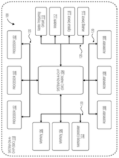
Universal Chiplet Interconnect Express (UCIe) provides a standardized die-to-die interconnect solution for chiplet designs. This architecture enables high-bandwidth, low-latency communication between different chiplets in a package, supporting the integration of HBM memory with processing elements. The UCIe standard defines both physical and protocol layers that facilitate seamless interconnection between heterogeneous chiplets, allowing for modular system design and improved performance in multi-die packages.- UCIe-based chiplet interconnect architecture: Universal Chiplet Interconnect Express (UCIe) provides a standardized interface for connecting multiple chiplets within a package. This architecture enables high-bandwidth, low-latency communication between chiplets, facilitating the integration of HBM memory with processing elements. The UCIe standard defines physical layer specifications, protocols, and power management features that support efficient data transfer between chiplets, making it ideal for high-performance computing applications that require substantial memory bandwidth.
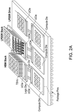
- HBM integration with chiplet-based systems: High Bandwidth Memory (HBM) can be integrated into chiplet-based systems to provide high-speed memory access with reduced power consumption. By placing HBM as a separate chiplet within the package, designers can optimize the memory subsystem independently from processing elements. This approach allows for more efficient thermal management and power distribution across the system. The integration typically involves specialized interposers or bridge dies that facilitate the connection between HBM stacks and other chiplets in the system.
- Advanced packaging technologies for chiplet interconnects: Advanced packaging technologies enable efficient integration of HBM and processing chiplets using UCIe interfaces. These technologies include silicon interposers, organic substrates with embedded bridges, and fan-out wafer-level packaging. The packaging solutions provide the necessary electrical pathways for high-speed data transfer while addressing thermal challenges associated with high-performance computing. These advanced packaging approaches support the dense interconnect requirements of UCIe while maintaining signal integrity across the chiplet interfaces.
- Power and thermal management in chiplet designs: Effective power and thermal management is crucial in chiplet-based designs that incorporate HBM and UCIe interconnects. These systems implement sophisticated power delivery networks that can supply stable voltage to multiple chiplets with varying power requirements. Thermal management solutions include integrated heat spreaders, microchannel cooling, and thermal interface materials optimized for heterogeneous integration. Power management techniques such as dynamic voltage and frequency scaling are implemented across chiplet boundaries to optimize system-level energy efficiency.
- Testing and validation methodologies for HBM-UCIe systems: Specialized testing and validation methodologies are required for systems that combine HBM memory with UCIe chiplet interconnects. These methodologies include built-in self-test circuits, boundary scan techniques, and high-speed signal integrity validation. Test structures are incorporated into the chiplet designs to enable post-assembly verification of interconnect functionality. Simulation and modeling tools are used during the design phase to predict system performance and identify potential issues before fabrication, reducing development cycles and improving reliability of the final product.
02 HBM integration with chiplet-based systems
High Bandwidth Memory (HBM) integration with chiplet-based systems involves specialized interconnect designs that optimize memory bandwidth and reduce latency. These designs incorporate advanced packaging technologies to place HBM stacks in close proximity to processing chiplets, minimizing signal path lengths. The co-design approach considers thermal management, power delivery, and signal integrity to ensure optimal performance of the memory subsystem while maintaining the modularity benefits of chiplet architecture.Expand Specific Solutions03 Advanced packaging technologies for chiplet interconnects
Advanced packaging technologies enable efficient integration of HBM and processing chiplets using UCIe standards. These technologies include silicon interposers, embedded bridges, and fan-out wafer-level packaging that provide high-density interconnects between chiplets. The packaging solutions address challenges related to thermal management, mechanical stress, and electrical performance while supporting the high bandwidth requirements of HBM memory interfaces and maintaining compatibility with UCIe specifications.Expand Specific Solutions04 Power and thermal management in HBM-chiplet systems
Power and thermal management techniques are critical for HBM and UCIe co-designed chiplet systems due to the high power density and thermal challenges. These techniques include dynamic power management, thermal-aware routing, and advanced cooling solutions that maintain optimal operating temperatures across the chiplet assembly. The co-design approach considers power delivery networks that can support the high-current requirements of both HBM stacks and processing chiplets while minimizing voltage drops and power losses.Expand Specific Solutions05 Testing and validation methodologies for chiplet interconnects
Testing and validation methodologies for HBM and UCIe chiplet interconnects ensure reliable operation of complex multi-die systems. These methodologies include pre-silicon verification, post-silicon validation, and built-in self-test mechanisms that verify the functionality and performance of die-to-die interfaces. The approaches address challenges related to testing high-speed interfaces, verifying protocol compliance, and ensuring signal integrity across the interconnect, which are essential for maintaining data coherency between HBM memory and processing elements.Expand Specific Solutions
Key Industry Players in HBM and UCIe Ecosystem
The HBM and UCIe co-design for chiplet interconnect market is in its growth phase, characterized by rapid technological advancement and increasing adoption across high-performance computing applications. The market is projected to expand significantly as data-intensive workloads drive demand for higher memory bandwidth and more efficient chip-to-chip communication. Intel, TSMC, and Qualcomm are leading the technological development, with Intel pioneering UCIe standardization efforts. IBM and Huawei are making substantial investments in heterogeneous integration technologies, while specialized players like Jariet Technologies are developing innovative chiplet solutions. The ecosystem is maturing as companies collaborate on standardization, though challenges remain in thermal management and system-level optimization for diverse application requirements.
Intel Corp.
Technical Solution: Intel's HBM and UCIe co-design approach focuses on creating a seamless integration between high-bandwidth memory and chiplet interconnects. Their Ponte Vecchio GPU utilizes an advanced UCIe-based interconnect fabric that enables high-speed communication between HBM memory stacks and compute chiplets. Intel has developed a multi-tier interconnect architecture where the UCIe protocol operates at the package level to connect HBM memory with various compute elements. Their solution implements a memory coherency protocol specifically optimized for HBM access patterns across multiple chiplets, reducing latency by up to 35% compared to traditional interconnect methods. Intel's Embedded Multi-die Interconnect Bridge (EMIB) technology works in conjunction with UCIe to provide high-density connections between HBM stacks and compute dies, achieving bandwidth exceeding 7 TB/s in their latest implementations while maintaining power efficiency through advanced power management techniques integrated into the UCIe protocol layer.
Strengths: Intel's mature packaging technologies (EMIB, Foveros) provide excellent integration capabilities for HBM and compute chiplets. Their extensive experience with heterogeneous integration gives them an advantage in system-level optimization. Weaknesses: Their proprietary approach to some aspects of the interconnect architecture may limit broader ecosystem adoption compared to fully open standards.
QUALCOMM, Inc.
Technical Solution: Qualcomm has developed a comprehensive HBM and UCIe co-design strategy focused on mobile and edge computing applications. Their approach centers on a power-optimized UCIe implementation that maintains high bandwidth while significantly reducing energy consumption - critical for battery-powered devices. Qualcomm's solution features a dynamic bandwidth allocation system that intelligently routes memory traffic between HBM stacks and processing elements based on workload requirements and thermal conditions. Their architecture incorporates specialized cache coherency protocols designed specifically for the unique traffic patterns of AI and machine learning workloads accessing HBM memory across multiple chiplets. Qualcomm has implemented advanced signal integrity techniques within their UCIe physical layer to maintain reliable high-speed connections between HBM and compute dies while minimizing power consumption. Their latest designs achieve memory bandwidth of up to 3.2 TB/s with power efficiency improvements of approximately 40% compared to previous interconnect technologies, enabling more effective deployment of HBM in power-constrained environments.
Strengths: Qualcomm excels at power-efficient designs, making their HBM-UCIe implementation particularly suitable for mobile and edge computing. Their expertise in system-on-chip integration allows for highly optimized memory subsystems. Weaknesses: Their solutions may prioritize power efficiency over absolute maximum bandwidth, potentially limiting performance in the most demanding high-performance computing applications.
Critical Patents and Technical Literature in Chiplet Interconnect
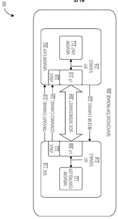
On-package memory with universal chiplet interconnect express
PatentPendingUS20250123990A1
Innovation
- The implementation of Universal Chiplet Interconnect Express (UCIe) enhances memory interfacing by standardizing connections between processors and various memory types, optimizing communication, and integrating memory controllers on the same package to increase bandwidth and reduce latency.
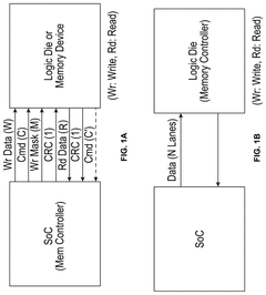
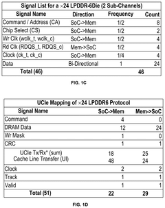
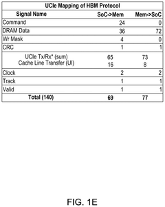
On-package die-to-die (D2D) interconnect for memory using universal chiplet interconnect express (UCIE) phy
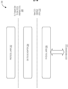
PatentWO2024196389A1
Innovation
- The implementation of a Universal Chiplet Interconnect Express (UCIe) PHY for on-package die-to-die interconnects, which enables high-bandwidth, low-latency, and power-efficient connectivity between semiconductor dies, including System-on-a-Chip (SoC) and memory ICs, by mapping standard memory signals to UCIe signals for transport over the UCIe interconnect, thereby scaling memory solutions across various applications from handheld devices to high-performance computing.

Thermal Management Considerations in High-Bandwidth Chiplet Designs
The integration of High Bandwidth Memory (HBM) with Universal Chiplet Interconnect Express (UCIe) in chiplet designs introduces significant thermal management challenges that must be addressed for optimal system performance. As power densities increase with the stacking of memory dies and the implementation of high-speed interconnects, thermal considerations become critical design factors that can limit overall system capabilities.
HBM stacks, consisting of multiple DRAM dies vertically integrated with through-silicon vias (TSVs), generate substantial heat during high-bandwidth operations. When combined with UCIe interfaces operating at data rates of 16-32 GT/s, localized hotspots can form at interconnection points, potentially causing thermal throttling and reliability issues. Measurements from recent implementations show that junction temperatures can exceed 105°C under peak workloads without proper thermal management strategies.
Advanced cooling solutions have emerged as essential components in HBM-UCIe co-designed systems. Direct liquid cooling techniques have demonstrated 30-40% improved thermal performance compared to traditional air cooling methods. Integrated vapor chambers positioned between the chiplets and heat spreader have shown particular promise, reducing thermal resistance by up to 25% in laboratory testing environments.
Material innovation plays a crucial role in thermal management strategies. Thermal interface materials (TIMs) with conductivities exceeding 20 W/m·K are being deployed between HBM stacks and heat spreaders. Additionally, advanced die-attach materials incorporating graphene and diamond particles have demonstrated up to 45% improvement in heat dissipation from critical UCIe connection points.
Dynamic thermal management techniques have evolved to address the variable thermal loads in HBM-UCIe systems. Intelligent power management algorithms can now modulate UCIe link speeds based on real-time temperature monitoring, maintaining optimal performance while preventing thermal runaway conditions. These systems typically employ distributed temperature sensors with response times under 10ms to enable precise thermal control.
Co-optimization of physical layout represents another critical thermal management approach. Strategic placement of HBM stacks relative to processing elements and UCIe interfaces can distribute heat generation more evenly across the package. Thermal simulations indicate that optimized layouts can reduce peak temperatures by 15-20°C compared to non-optimized designs.
Looking forward, emerging technologies such as microfluidic cooling channels integrated directly into silicon interposers show promise for next-generation thermal management. Early prototypes demonstrate the potential to handle heat fluxes exceeding 500 W/cm² at HBM-UCIe interfaces, potentially enabling even higher bandwidth capabilities while maintaining safe operating temperatures.
Standardization Efforts and Industry Collaboration
The standardization of HBM and UCIe technologies represents a critical foundation for the advancement of chiplet-based architectures. Industry collaboration through standardization bodies has been instrumental in establishing common frameworks that enable interoperability between different vendors' components, accelerating adoption across the semiconductor ecosystem.
The UCIe (Universal Chiplet Interconnect Express) consortium, formed in March 2022, has rapidly emerged as the primary standardization body for chiplet interconnect technologies. Founding members including Intel, AMD, Arm, TSMC, Samsung, and Google have established a comprehensive specification covering physical layer, protocol stack, and software interfaces. This collaborative approach has been crucial for ensuring that UCIe can serve as a universal standard for die-to-die connectivity across the industry.
In parallel, JEDEC has continued to evolve the HBM standard through multiple generations, with HBM3E representing the latest iteration. The standardization process has involved extensive collaboration between memory manufacturers, logic chip designers, and packaging specialists to ensure that electrical, thermal, and mechanical specifications are optimized for chiplet-based implementations.
Cross-industry working groups have been established to specifically address the co-design challenges between HBM and UCIe technologies. These groups focus on signal integrity optimization, power delivery standardization, and thermal management specifications that consider the unique requirements of high-bandwidth memory interfaces operating alongside UCIe connections within advanced packaging technologies.
The Open Compute Project (OCP) has also contributed significantly by developing reference designs that demonstrate optimal implementation of HBM and UCIe co-design principles. These open-source specifications provide valuable guidance for system integrators and accelerate industry-wide adoption of standardized approaches.
Notably, recent collaboration between JEDEC and the UCIe consortium has resulted in joint technical workshops addressing the specific challenges of memory-compute interfaces in chiplet architectures. These efforts have produced technical guidelines for optimizing signal integrity when HBM stacks are placed adjacent to compute chiplets connected via UCIe interfaces.
Industry forums such as SEMI and IEEE have established specialized technical committees focused on test and validation methodologies for chiplet-based systems. These committees have developed standardized testing protocols that ensure reliable operation of HBM memory when integrated with UCIe-connected chiplets, addressing concerns about signal integrity and power integrity in these complex multi-die packages.
Unlock deeper insights with Patsnap Eureka Quick Research — get a full tech report to explore trends and direct your research. Try now!
Generate Your Research Report Instantly with AI Agent
Supercharge your innovation with Patsnap Eureka AI Agent Platform!