

UCIe Chiplet Interconnect Power Integrity And Decoupling Solutions
SEP 1, 20259 MIN READ
Generate Your Research Report Instantly with AI Agent
Patsnap Eureka helps you evaluate technical feasibility & market potential.
UCIe Chiplet Interconnect Background and Objectives
Universal Chiplet Interconnect Express (UCIe) represents a significant advancement in semiconductor integration technology, emerging as a response to the growing challenges in traditional monolithic chip design. The evolution of semiconductor technology has historically followed Moore's Law, with transistor density doubling approximately every two years. However, as process nodes have shrunk below 7nm, the industry has encountered physical limitations and exponentially increasing costs, necessitating alternative approaches to continue performance scaling.
Chiplet architecture has emerged as a promising solution, allowing complex systems to be built from smaller, specialized silicon dies interconnected on a package substrate. This modular approach enables mixing of process nodes, reduces manufacturing costs, and improves yield rates compared to large monolithic designs. The development of chiplet technology can be traced back to early multi-chip module approaches, but has gained significant momentum in the past decade with implementations from AMD, Intel, and other major semiconductor companies.
UCIe specifically addresses the critical need for standardization in chiplet interconnect technology. Prior to UCIe, chiplet implementations were largely proprietary, creating ecosystem fragmentation and limiting interoperability between components from different vendors. Announced in March 2022 by a consortium of industry leaders including Intel, AMD, Arm, TSMC, and Samsung, UCIe aims to establish an open, universal interconnect standard for chiplet-based designs.
The primary objective of UCIe is to enable a robust chiplet ecosystem where dies from different vendors can seamlessly work together within a single package. This standard defines both the physical layer specifications and protocols for die-to-die communication, supporting both standard and advanced packaging technologies. UCIe accommodates different interconnect topologies and provides specifications for both the physical and protocol layers of chiplet communication.
Power integrity and decoupling solutions represent critical challenges within the UCIe framework. As data rates increase (targeting up to 32 GT/s in initial specifications), power delivery network (PDN) design becomes increasingly complex. The standard must address issues of power supply noise, ground bounce, and signal integrity across die boundaries while maintaining compatibility with various packaging technologies and thermal solutions.
The technical goals for UCIe power integrity solutions include minimizing power consumption while maximizing data transfer rates, ensuring signal integrity across different chiplet configurations, and maintaining backward compatibility with existing packaging technologies. Additionally, the standard aims to support future scaling of bandwidth demands while providing a clear migration path for implementation across various process nodes and packaging technologies.
Market Demand Analysis for Chiplet Integration
The chiplet integration market is experiencing unprecedented growth, driven by the semiconductor industry's shift from monolithic designs to disaggregated architectures. This transition is primarily fueled by the slowing of Moore's Law and the increasing costs associated with advanced process nodes. According to recent industry analyses, the global chiplet market is projected to grow at a CAGR of 40% from 2023 to 2028, reaching significant market valuation as heterogeneous integration becomes mainstream.
Power integrity and decoupling solutions for UCIe (Universal Chiplet Interconnect Express) represent a critical segment within this expanding market. As chiplet designs become more complex, with multiple dies from different process nodes integrated onto a single package, managing power delivery and signal integrity becomes increasingly challenging. Industry surveys indicate that over 65% of system designers identify power integrity as a primary concern in chiplet-based designs.
The demand for UCIe power integrity solutions is particularly strong in high-performance computing, data centers, and AI accelerator markets. These sectors require increasingly powerful systems while maintaining energy efficiency. The data center market alone is expected to consume nearly half of all chiplet-based solutions by 2025, with power integrity being a key specification requirement for these implementations.
Telecommunications and networking equipment manufacturers represent another significant market segment, as they transition to chiplet-based designs for next-generation infrastructure. These applications demand robust power integrity solutions to ensure reliable operation under varying workloads and environmental conditions.
Consumer electronics manufacturers are also showing increased interest in chiplet technology, particularly for premium mobile devices and AR/VR equipment where performance per watt is crucial. This market segment is expected to grow substantially as chiplet integration costs decrease and standardization efforts mature.
Geographically, North America and East Asia dominate the market demand, with major semiconductor companies and system integrators heavily investing in chiplet technology. Europe is showing accelerated adoption rates, particularly in automotive and industrial applications where reliability requirements are stringent.
The market is further stimulated by industry consortiums and standardization efforts around UCIe, which has gained support from major players including Intel, AMD, Arm, TSMC, and Samsung. This collaborative approach is reducing barriers to adoption and creating a more unified ecosystem for chiplet integration.
Customer requirements are increasingly focused on solutions that address both the electrical and thermal aspects of power integrity, as power density in advanced packages continues to rise. This has created market opportunities for specialized design tools, advanced packaging materials, and novel decoupling technologies specifically optimized for chiplet architectures.
Power Integrity Challenges in UCIe Implementation
Power integrity has emerged as a critical challenge in UCIe (Universal Chiplet Interconnect Express) implementation, particularly as chiplet-based designs push the boundaries of high-speed communication while maintaining strict power constraints. The primary challenge stems from the inherent nature of UCIe's high-speed interfaces, which operate at data rates exceeding 16 Gbps, creating significant power distribution network (PDN) design complexities.
Signal integrity and power integrity are tightly coupled in UCIe implementations. As signals transition at high frequencies, they generate substantial simultaneous switching noise (SSN) that can propagate through the power delivery network, causing voltage fluctuations that compromise signal quality. This challenge is exacerbated in multi-chiplet designs where power must be distributed across multiple die with varying power requirements.
The physical implementation of UCIe introduces unique power integrity challenges. The fine-pitch microbumps and through-silicon vias (TSVs) used for chiplet interconnection create impedance discontinuities and current crowding effects that can lead to localized heating and voltage drops. These effects become more pronounced as UCIe implementations push toward higher bandwidth densities and lower power envelopes.
Decoupling capacitor placement presents another significant challenge. The limited space available between chiplets and the need to minimize parasitic inductance requires innovative approaches to decoupling capacitor integration. Traditional decoupling strategies often prove insufficient for the fast transient currents characteristic of UCIe interfaces.
Power delivery to the die-to-die (D2D) interfaces is particularly challenging due to the high current densities required. The UCIe standard's support for both standard and advanced packages creates varying thermal and electrical constraints that must be addressed through careful power integrity analysis and design.
Electromagnetic interference (EMI) and crosstalk between power and signal lines represent additional challenges. The dense routing required for UCIe implementations increases the likelihood of coupling effects that can degrade both power and signal integrity, particularly in the retimer and PHY circuits that are critical to UCIe operation.
Thermal management intersects with power integrity challenges, as hotspots can create localized resistance changes that affect voltage distribution. The heterogeneous integration of chiplets with different power densities and thermal characteristics compounds this challenge, requiring holistic thermal-electrical co-design approaches.
As UCIe adoption grows, these power integrity challenges will require increasingly sophisticated solutions that balance performance, power efficiency, and manufacturability while maintaining compatibility with the evolving UCIe standard specifications.
Current Power Integrity and Decoupling Solutions
01 Power integrity solutions for UCIe chiplet interconnects
Various power integrity solutions are implemented in UCIe chiplet interconnects to ensure stable power delivery across multiple dies. These solutions include specialized power distribution networks, decoupling capacitors, and voltage regulation techniques that minimize power fluctuations at the interconnect boundaries. Advanced power management circuits monitor and adjust power delivery in real-time to maintain signal integrity across the high-speed interconnects between chiplets.- Power integrity solutions for UCIe chiplet interconnects: Various power integrity solutions are implemented in UCIe chiplet interconnects to ensure stable power delivery across multiple dies. These solutions include specialized power distribution networks, decoupling capacitors, and voltage regulation techniques that minimize power fluctuations during high-speed data transfer between chiplets. Advanced power integrity management systems monitor and adjust power delivery in real-time to maintain signal integrity across the interconnect interfaces.
- Thermal management for UCIe chiplet power integrity: Thermal management techniques are crucial for maintaining power integrity in UCIe chiplet interconnects. These include integrated thermal sensors, advanced cooling solutions, and thermal-aware power management algorithms that prevent thermal hotspots from affecting signal integrity. By effectively managing heat distribution across chiplets, these solutions ensure consistent electrical performance of the interconnects even under varying computational loads.
- Signal and power integrity co-design for UCIe implementations: Co-design methodologies that simultaneously address signal and power integrity are essential for UCIe chiplet interconnects. These approaches include integrated modeling of power delivery networks alongside signal paths, impedance matching techniques, and simultaneous switching noise mitigation. Advanced electromagnetic simulation tools help designers optimize both power and signal integrity parameters to ensure reliable high-speed communication between chiplets while maintaining clean power delivery.
- Power integrity testing and validation for UCIe interfaces: Specialized testing and validation methodologies are developed for verifying power integrity in UCIe chiplet interconnects. These include on-die measurement circuits, built-in self-test mechanisms, and comprehensive validation frameworks that characterize power delivery under various operating conditions. Advanced test equipment and protocols help identify potential power integrity issues before they affect system performance, ensuring robust operation of multi-chiplet systems.
- Advanced packaging solutions for UCIe power integrity: Innovative packaging technologies are employed to enhance power integrity in UCIe chiplet interconnects. These include advanced substrate designs with embedded power planes, through-silicon vias (TSVs) for efficient power delivery, and novel interposer technologies that optimize power distribution. These packaging solutions minimize power delivery network impedance and reduce voltage drops across chiplet interfaces, ensuring stable operation of high-performance multi-chiplet systems.
02 Signal integrity and noise reduction in UCIe implementations
Signal integrity is maintained in UCIe chiplet interconnects through various noise reduction techniques. These include electromagnetic interference (EMI) shielding, ground plane optimization, and specialized routing methodologies that minimize crosstalk between adjacent interconnect channels. Advanced equalization techniques compensate for signal degradation across the interconnect, while impedance matching ensures optimal signal transfer between chiplets with different power domains.Expand Specific Solutions03 Thermal management for UCIe power integrity
Thermal management solutions are critical for maintaining power integrity in UCIe chiplet interconnects. These include integrated thermal sensors, dynamic thermal management systems, and specialized materials with enhanced thermal conductivity. Advanced cooling solutions such as microchannel liquid cooling and phase-change materials help dissipate heat from high-density interconnect regions. Thermal-aware power management algorithms adjust power delivery based on temperature conditions to prevent thermal-induced signal degradation.Expand Specific Solutions04 Power delivery network design for UCIe chiplets
Specialized power delivery network (PDN) designs for UCIe chiplet interconnects include multi-layer power distribution, integrated voltage regulators, and optimized power grid architectures. These designs incorporate strategically placed power and ground planes to minimize impedance and ensure uniform power distribution across the interconnect. Advanced PDN modeling techniques simulate power delivery under various operating conditions to identify and mitigate potential integrity issues before fabrication.Expand Specific Solutions05 Testing and validation methodologies for UCIe power integrity
Comprehensive testing and validation methodologies ensure power integrity in UCIe chiplet interconnects. These include specialized test structures, on-die measurement circuits, and advanced simulation techniques that model power delivery across multiple chiplets. Automated test equipment performs power integrity measurements under various operating conditions, while built-in self-test (BIST) circuits continuously monitor power integrity during operation. Post-silicon validation techniques identify and characterize power integrity issues in manufactured chiplets.Expand Specific Solutions
Key Industry Players in UCIe Ecosystem
The UCIe Chiplet Interconnect Power Integrity and Decoupling Solutions market is currently in its growth phase, with increasing adoption across high-performance computing applications. The market is projected to expand significantly as chiplet architecture becomes more prevalent in addressing semiconductor scaling challenges. Intel leads the technological development as a founding member of the UCIe consortium, with TSMC, GlobalFoundries, and Samsung Electronics providing critical manufacturing capabilities. Qualcomm and IBM contribute significant IP in interconnect technologies, while research institutions like Industrial Technology Research Institute and Institute of Microelectronics of Chinese Academy of Sciences advance fundamental research. The technology is approaching maturity for early applications but continues to evolve as power integrity challenges become more complex with increasing chiplet integration densities.
Intel Corp.
Technical Solution: Intel's UCIe chiplet interconnect power integrity solution focuses on advanced power delivery network (PDN) design and decoupling strategies. Their approach includes multi-layer embedded capacitance in the substrate, strategically placed microbumps for power distribution, and optimized C4 bump layouts to minimize power delivery impedance[1]. Intel implements a hierarchical decoupling strategy with on-die decoupling capacitors (ODCs), package decoupling capacitors, and board-level capacitors to address different frequency bands of power noise[2]. Their PDN design incorporates sophisticated modeling techniques that account for simultaneous switching noise and resonance effects across the entire chiplet ecosystem. Intel has also developed specialized EDA tools for power integrity simulation that can model the complex interactions between multiple chiplets in a UCIe implementation[3]. Their solution includes adaptive voltage regulation techniques that respond to workload changes across different chiplets to maintain signal integrity while optimizing power consumption.
Strengths: Industry-leading expertise in chiplet integration with proven implementation in products like Ponte Vecchio; comprehensive PDN modeling capabilities across multiple domains; established manufacturing infrastructure. Weaknesses: Proprietary approaches may limit ecosystem adoption; higher implementation costs compared to some competitors; power management solutions may be optimized primarily for x86 architectures.
International Business Machines Corp.
Technical Solution: IBM's UCIe chiplet interconnect power integrity solution leverages their extensive experience in high-performance computing systems. Their approach centers on a holistic power distribution architecture that integrates advanced 2.5D and 3D packaging technologies with sophisticated power management techniques[1]. IBM implements distributed point-of-load voltage regulators positioned strategically near high-power chiplets to minimize IR drop and improve transient response[2]. Their decoupling solution incorporates multi-layer ceramic capacitors (MLCCs) embedded within the package substrate, combined with thin-film capacitors integrated directly into the interposer structure. IBM's power integrity design includes advanced electromagnetic simulation models that account for mutual inductance effects between adjacent chiplets and power/ground planes[3]. They've developed specialized silicon-proven power integrity verification methodologies that address the unique challenges of heterogeneous integration, including thermal-aware power modeling that accounts for hotspot formation at chiplet interfaces and its impact on signal integrity across UCIe links.
Strengths: Deep expertise in high-performance computing systems; advanced packaging technologies with proven power delivery solutions; comprehensive simulation and modeling capabilities. Weaknesses: Solutions may be optimized primarily for enterprise/HPC applications rather than broader markets; potentially higher implementation costs; more complex integration requirements compared to some competitors.
Critical Patents and Research in UCIe Power Management
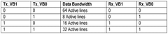
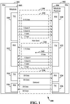
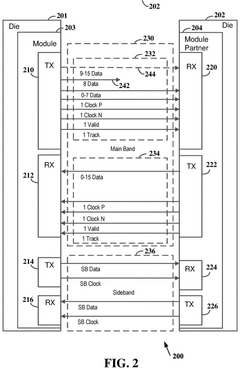
Variable link width in two directions for main band chip module connection
PatentWO2024226177A1
Innovation
- Implementing a variable link width mechanism in both directions of the main band connection, allowing for dynamic adjustment of the number of active data lanes based on requirements through a sideband communication protocol, enabling independent configuration of transmit and receive data lines to optimize power usage and data rates.

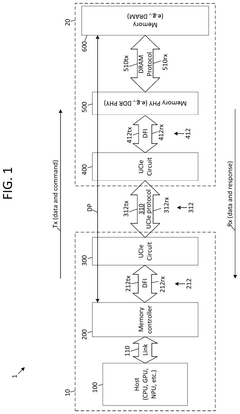
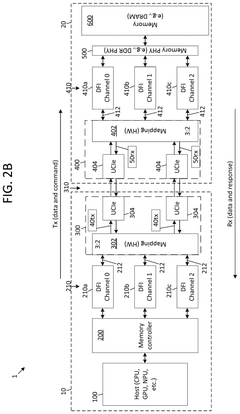
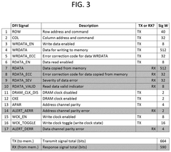
SYSTEMS AND METHODS FOR TRANSMITTING AND RECEIVING DOUBLE DATA RATE (DDR) PHYSICAL (PHY) INTERFACE (DFI) SIGNALS USING UNIVERSAL CHIPLET INTERCONNECT EXPRESS (UCIe)
PatentPendingUS20250258786A1
Innovation
- The use of a universal chiplet interconnect express (UCIe) interface for die-to-die communication, which converts DDR PHY interface signals to UCIe signals based on specific mappings, reducing power consumption and enhancing scalability by integrating fewer UCIe modules compared to traditional DDR PHY methods.

Thermal Management Considerations for UCIe Implementations
Thermal management represents a critical consideration in UCIe (Universal Chiplet Interconnect Express) implementations, particularly when addressing power integrity and decoupling solutions. As chiplet architectures continue to evolve with higher integration densities and increased power requirements, thermal challenges have emerged as significant limiting factors for system performance and reliability.
The thermal characteristics of UCIe implementations are directly influenced by the power distribution network design and decoupling capacitor placement. High-frequency switching activities across chiplet interfaces generate localized hotspots that can compromise signal integrity if not properly managed. These thermal gradients may induce mechanical stress at interconnect boundaries, potentially leading to reliability concerns such as solder joint fatigue or delamination.
Current UCIe specifications define thermal design power (TDP) guidelines, but practical implementations require more sophisticated approaches. Advanced thermal simulation models that incorporate both electrical and thermal co-simulation have become essential tools for predicting temperature profiles across chiplet interfaces. These models must account for the unique thermal resistance characteristics of microbump arrays and the thermal conductivity limitations of organic substrate materials.
Cooling solutions for UCIe implementations have evolved beyond traditional approaches. Direct liquid cooling technologies targeting the chiplet interface regions have demonstrated superior thermal performance compared to conventional heat sink solutions. Some leading implementations utilize integrated microfluidic channels within the package substrate to extract heat directly from high-power density regions near the die-to-die interfaces.
Thermal-aware floor planning has emerged as a critical design methodology for UCIe implementations. Strategic placement of high-power components and thermal management structures can significantly improve heat dissipation pathways. The industry has observed up to 30% improvement in thermal performance through optimized component placement that considers both electrical and thermal constraints simultaneously.
Material innovation plays a crucial role in addressing thermal challenges. Advanced thermal interface materials (TIMs) with enhanced thermal conductivity properties are being developed specifically for chiplet applications. These materials must maintain performance while accommodating the mechanical stress induced by thermal cycling between heterogeneous components with different coefficients of thermal expansion.
Looking forward, emerging technologies such as embedded cooling and phase-change materials show promise for next-generation UCIe implementations. These approaches aim to manage thermal challenges while maintaining the electrical performance advantages that make chiplet architectures attractive for high-performance computing applications.
Manufacturing and Testing Standards for UCIe Chiplets
The manufacturing and testing standards for UCIe chiplets represent a critical framework ensuring interoperability and reliability across multi-vendor chiplet ecosystems. These standards encompass rigorous specifications for fabrication processes, quality control measures, and validation methodologies specifically designed to address power integrity challenges in UCIe implementations.
Manufacturing standards for UCIe chiplets mandate precise specifications for bump pitch, die thickness, and substrate materials that directly impact power delivery network (PDN) performance. Current standards specify bump pitches ranging from 25-55μm, with strict tolerances of ±2μm to ensure consistent power distribution across the interconnect. These manufacturing guidelines also define requirements for RDL (Redistribution Layer) geometries and metallization processes that are essential for maintaining low-impedance power delivery paths.
Testing protocols for UCIe chiplets incorporate specialized methodologies for evaluating power integrity across the die-to-die interfaces. These include Time Domain Reflectometry (TDR) measurements to characterize impedance profiles, and Vector Network Analyzer (VNA) testing to assess S-parameters across the frequency spectrum relevant to UCIe operations (typically 0-20GHz). The standards define pass/fail criteria for power supply noise, with maximum allowable ripple typically constrained to less than 3% of nominal supply voltage.
Decoupling capacitor integration receives particular attention in UCIe manufacturing standards, with specifications for both on-die and package-level decoupling solutions. The standards define minimum capacitance densities (typically 10-30nF/mm²) and maximum ESR/ESL values to ensure adequate transient response. Manufacturing processes must accommodate these components while maintaining strict co-planarity requirements across the chiplet interface.
Quality assurance protocols for UCIe implementations include specialized tests for power integrity under various operating conditions. These encompass thermal cycling (-40°C to +125°C), voltage margining (±10% of nominal), and accelerated life testing to verify long-term reliability of power delivery networks. The standards also define methodologies for in-situ power integrity monitoring during high-speed data transmission, with requirements for built-in self-test (BIST) capabilities.
Compliance testing frameworks ensure that manufactured chiplets meet UCIe power integrity specifications before integration into multi-die packages. These frameworks include standardized test fixtures, reference PDN designs, and measurement procedures that enable consistent evaluation across different manufacturing facilities. The standards also define certification processes that vendors must complete to ensure their chiplets will function reliably when integrated with components from other manufacturers in heterogeneous systems.
Unlock deeper insights with Patsnap Eureka Quick Research — get a full tech report to explore trends and direct your research. Try now!
Generate Your Research Report Instantly with AI Agent
Supercharge your innovation with Patsnap Eureka AI Agent Platform!