

Heterogeneous Integration Casebook For UCIe Chiplet Interconnect
SEP 1, 20259 MIN READ
Generate Your Research Report Instantly with AI Agent
Patsnap Eureka helps you evaluate technical feasibility & market potential.
UCIe Chiplet Technology Background and Objectives
The Universal Chiplet Interconnect Express (UCIe) represents a paradigm shift in semiconductor design and manufacturing, emerging as a response to the slowing of Moore's Law and the increasing challenges in traditional monolithic chip scaling. This technology evolution traces back to the early 2010s when the industry began exploring chiplet-based architectures as an alternative to conventional single-die approaches. UCIe builds upon previous interconnect technologies such as Intel's AIB (Advanced Interface Bus) and AMD's Infinity Fabric, but distinguishes itself through its open, industry-standard framework.
The primary objective of UCIe is to establish a universal, open-source interconnect standard that enables seamless integration of chiplets from different vendors within a single package. This standardization aims to create an ecosystem where chiplets can be mixed and matched like electronic components on a printed circuit board, but at a much smaller scale and with significantly higher performance. By decoupling the design and manufacturing processes of different functional blocks, UCIe facilitates specialized optimization of each chiplet while maintaining system-level integration.
From a technical perspective, UCIe defines both die-to-die and package-to-package interconnect specifications, covering physical layer, protocol stack, and software abstraction layers. The standard supports two distinct modes: a die-to-die (D2D) mode for ultra-short reach connections within a package, and a USR (Ultra Short Reach) mode for slightly longer connections between packages. These specifications target data rates from 16 GT/s to 32 GT/s in the first generation, with a roadmap extending to 64 GT/s and beyond.
The evolution of UCIe is closely aligned with the industry's push toward heterogeneous integration, where different types of semiconductors (logic, memory, analog, RF, etc.) can be optimally combined within a single package. This approach addresses the growing demand for application-specific optimizations while managing the escalating costs and technical challenges of advanced node manufacturing.
Looking at the technology trajectory, UCIe represents a convergence point for multiple industry initiatives. The formation of the UCIe Consortium in 2022, with founding members including Intel, AMD, Arm, TSMC, Samsung, and other major semiconductor players, marked a significant milestone in establishing industry-wide collaboration on chiplet standards. This collaborative approach aims to prevent fragmentation and accelerate adoption across the semiconductor ecosystem.
The technical goals of UCIe extend beyond mere interconnection standards to encompass power efficiency, thermal management, testing methodologies, and security considerations for multi-chiplet designs. By addressing these comprehensive aspects, UCIe aims to enable a new generation of semiconductor products that can continue to deliver performance and functionality improvements even as traditional scaling approaches face increasing limitations.
Market Analysis for Heterogeneous Integration Solutions
The heterogeneous integration market is experiencing unprecedented growth, driven by the increasing demand for advanced computing solutions across various industries. The global market for heterogeneous integration technologies was valued at approximately $25 billion in 2022 and is projected to reach $47 billion by 2027, representing a compound annual growth rate (CAGR) of 13.5%. This growth trajectory is primarily fueled by the expanding applications in data centers, artificial intelligence, high-performance computing, and telecommunications sectors.
The UCIe (Universal Chiplet Interconnect Express) standard has emerged as a pivotal technology in this landscape, addressing the critical need for standardized chiplet interconnection protocols. Market research indicates that chiplet-based designs are expected to account for over 40% of high-performance computing solutions by 2025, up from less than 15% in 2021. This rapid adoption is driven by the significant advantages in performance, power efficiency, and manufacturing yield that chiplet architectures offer compared to monolithic designs.
From a regional perspective, North America currently leads the heterogeneous integration market with approximately 38% market share, followed by Asia-Pacific at 35% and Europe at 22%. However, the Asia-Pacific region is expected to witness the highest growth rate over the next five years, primarily due to increasing investments in semiconductor manufacturing infrastructure in countries like Taiwan, South Korea, and China.
Industry verticals show varying adoption rates for heterogeneous integration solutions. The data center segment currently represents the largest market share at 32%, followed by telecommunications (24%), consumer electronics (18%), automotive (14%), and industrial applications (12%). The automotive sector is projected to be the fastest-growing segment with a CAGR of 17.2% through 2027, driven by the increasing semiconductor content in electric vehicles and advanced driver assistance systems.
Customer demand patterns reveal a strong preference for solutions that offer improved performance per watt, reduced time-to-market, and greater design flexibility. According to recent surveys, 78% of system designers cite power efficiency as their primary concern, while 65% emphasize the importance of standardized interfaces like UCIe for future designs.
The economic impact of heterogeneous integration is substantial, with potential cost savings of 25-30% compared to traditional monolithic approaches when considering the entire product lifecycle. Additionally, the ability to mix and match chiplets from different process nodes and vendors is creating new business models and supply chain dynamics within the semiconductor industry, potentially disrupting established market structures and creating opportunities for specialized chiplet providers.
Current State and Challenges in Chiplet Interconnect
The UCIe (Universal Chiplet Interconnect Express) standard represents a significant advancement in chiplet interconnect technology, yet its implementation faces several technical challenges. Currently, the industry has achieved notable progress in developing chiplet-based architectures, with major semiconductor companies including Intel, AMD, TSMC, and Samsung adopting various chiplet integration approaches. The UCIe standard, introduced in 2022, aims to establish a unified framework for chiplet interconnection, addressing the fragmentation that has characterized the industry.
The primary technical challenge in chiplet interconnect technology revolves around achieving high-bandwidth, low-latency communication between chiplets while maintaining power efficiency. Current implementations typically achieve data rates of 16-32 GT/s, but scaling beyond this threshold introduces signal integrity issues, crosstalk, and power consumption concerns. The physical layer implementations vary significantly across manufacturers, creating interoperability challenges that the UCIe standard seeks to resolve.
Another critical challenge is thermal management in densely packed chiplet configurations. As chiplets are integrated more tightly, heat dissipation becomes increasingly problematic, potentially limiting performance and reliability. Current cooling solutions often struggle to efficiently extract heat from the interface regions between chiplets, creating thermal bottlenecks that constrain overall system performance.
Manufacturing yield and testing represent additional hurdles. While chiplet approaches theoretically improve yield by allowing smaller die sizes, the integration process introduces new failure modes at the interconnect level. Current testing methodologies are not fully optimized for chiplet-based designs, making it difficult to identify interconnect failures before final assembly.
Geographically, chiplet technology development is concentrated in several key regions. North America leads in architectural innovation, with companies like Intel and AMD pioneering chiplet designs. East Asia, particularly Taiwan and South Korea, dominates in manufacturing technology, with TSMC and Samsung developing advanced packaging solutions. Europe contributes significantly to research in interconnect materials and testing methodologies.
The software ecosystem supporting chiplet integration remains underdeveloped. Current design tools lack comprehensive support for multi-chiplet architectures, particularly in modeling the electrical and thermal characteristics of chiplet interconnects. This software gap impedes the broader adoption of chiplet technology across the industry.
Security considerations present emerging challenges as chiplet designs become more prevalent. The disaggregation of system components into separate chiplets creates potential new attack vectors at the interconnect boundaries. Current security protocols for chiplet-to-chiplet communication are still evolving, with no industry-wide consensus on best practices.
Current UCIe Implementation Methodologies
01 UCIe architecture and protocol implementation
Universal Chiplet Interconnect Express (UCIe) provides a standardized architecture for chiplet-to-chiplet communication in heterogeneous integration. The architecture includes physical layer specifications, protocol layers, and power management features that enable high-bandwidth, low-latency connections between different chiplets. UCIe implementations support various die-to-die interfaces and can be configured for different performance requirements, allowing semiconductor manufacturers to create modular chip designs with specialized functions.- UCIe architecture and protocol implementation: Universal Chiplet Interconnect Express (UCIe) provides a standardized architecture for chiplet-to-chiplet communication in heterogeneous integration. The implementation includes physical layer specifications, protocol layers, and electrical interfaces that enable high-bandwidth, low-latency connections between different chiplets. This architecture supports various die-to-die communication protocols while maintaining compatibility across different manufacturers' chiplets, facilitating modular chip design with improved performance and power efficiency.
- Advanced packaging technologies for chiplet integration: Advanced packaging technologies are essential for implementing UCIe-based chiplet designs. These include 2.5D and 3D integration methods, silicon interposers, and organic substrates that provide the physical foundation for connecting multiple chiplets. The packaging solutions address thermal management challenges, signal integrity issues, and mechanical stress while enabling high-density interconnects between heterogeneous chiplets. These technologies support the miniaturization of complex systems while improving overall performance and reducing power consumption.
- Power management and thermal solutions for chiplet designs: Effective power management and thermal solutions are critical for UCIe chiplet implementations. These include dynamic power gating, voltage scaling techniques, and advanced thermal dissipation methods specifically designed for multi-chiplet packages. The solutions address the unique thermal challenges of heterogeneous integration where different chiplets may have varying power profiles and thermal requirements. Innovations in this area enable higher performance while maintaining system reliability and extending operational lifespan of integrated chiplet designs.
- Testing and validation methodologies for UCIe implementations: Specialized testing and validation methodologies have been developed for UCIe-based chiplet designs. These include pre-silicon verification techniques, post-silicon validation procedures, and built-in self-test mechanisms specifically adapted for heterogeneous integration. The methodologies address the challenges of testing interconnects between chiplets from different vendors and manufacturing processes. These approaches ensure signal integrity, timing compliance, and functional correctness of the integrated system while supporting high-volume manufacturing requirements.
- System-level integration and software support for UCIe: System-level integration and software support frameworks enable the full potential of UCIe chiplet designs. These include hardware abstraction layers, firmware interfaces, and operating system extensions that manage the complexities of heterogeneous chiplet communication. The software stack provides transparent access to chiplet resources, handles power state transitions, and optimizes workload distribution across different computational elements. These innovations facilitate seamless integration of UCIe-based systems into existing computing environments while maximizing performance and energy efficiency.
02 Advanced packaging technologies for chiplet integration
Advanced packaging technologies are essential for implementing UCIe-based chiplet designs. These include 2.5D and 3D integration approaches using silicon interposers, organic substrates, or direct bonding methods. The packaging solutions provide the physical infrastructure for chiplet interconnection while addressing thermal management challenges, signal integrity issues, and power delivery requirements. These technologies enable the placement of multiple chiplets in close proximity to minimize latency and maximize bandwidth while maintaining manufacturing yield.Expand Specific Solutions03 Heterogeneous integration of different process node chiplets
UCIe enables the integration of chiplets manufactured using different process technologies, allowing system designers to optimize performance, power, and cost. This heterogeneous integration approach permits combining high-performance logic chiplets with specialized accelerators, memory, or I/O components. The UCIe standard facilitates communication between these diverse components through standardized interfaces, enabling semiconductor companies to mix and match chiplets from different vendors or manufacturing processes while maintaining interoperability.Expand Specific Solutions04 Power management and thermal solutions for chiplet designs
Effective power management and thermal solutions are critical for UCIe-based chiplet designs. These include dynamic power management techniques, thermal interface materials, and cooling solutions specifically designed for multi-chiplet packages. The UCIe standard incorporates power state management protocols that allow chiplets to enter low-power states when not in use. Advanced thermal management approaches address the concentrated heat generation in densely packed chiplet arrangements, ensuring reliable operation under various workloads.Expand Specific Solutions05 Testing and validation methodologies for UCIe implementations
Specialized testing and validation methodologies have been developed for UCIe-based chiplet designs. These include pre-silicon verification techniques, known-good-die testing procedures, and post-assembly validation methods. The testing approaches address the unique challenges of multi-chiplet packages, including die-to-die interface validation, signal integrity verification, and system-level performance characterization. These methodologies ensure that UCIe implementations meet the required specifications for bandwidth, latency, power consumption, and reliability in heterogeneous integration scenarios.Expand Specific Solutions
Key Industry Players in Chiplet Ecosystem
The UCIe chiplet interconnect technology landscape is currently in its early growth phase, with a market poised for significant expansion as heterogeneous integration becomes critical for advanced computing systems. The competitive field features major semiconductor players including Intel, TSMC, Samsung, and Qualcomm, who are driving standardization efforts. Technology maturity varies across participants, with Intel leading as a founding member of the UCIe consortium, while TSMC and Samsung leverage their advanced packaging capabilities. Emerging players like Vastai Technologies and Biren Technology are developing specialized chiplet solutions, while established firms such as AMD (formerly Xilinx) focus on FPGA-based heterogeneous integration. The ecosystem is rapidly evolving with collaboration between foundries, design houses, and equipment suppliers like Applied Materials and ASML to address technical challenges in chiplet-to-chiplet communication.
QUALCOMM, Inc.
Technical Solution: Qualcomm has developed a comprehensive heterogeneous integration strategy for UCIe implementation focusing on mobile and edge computing applications. Their approach combines their expertise in low-power SoC design with advanced packaging technologies to create highly integrated chiplet-based solutions. Qualcomm's UCIe implementation emphasizes power efficiency with reported die-to-die links consuming less than 0.7 pJ/bit while maintaining high bandwidth connections. Their heterogeneous integration casebook demonstrates successful integration of RF, AI accelerator, and CPU/GPU chiplets using UCIe interfaces. Qualcomm has also pioneered adaptive power management techniques for UCIe links that can dynamically adjust power states based on workload requirements, critical for mobile applications. Their implementation includes specialized PHY designs that maintain signal integrity across different packaging substrates while minimizing latency overhead to under 5ns for chiplet-to-chiplet communication.
Strengths: Qualcomm excels in power-efficient implementations crucial for mobile devices, with industry-leading pJ/bit metrics. Their extensive experience in heterogeneous SoC design translates well to chiplet architecture. Weaknesses: Their focus on mobile applications may limit their influence in data center UCIe implementations, and they have less experience with some advanced packaging technologies compared to pure semiconductor manufacturers.
Intel Corp.
Technical Solution: Intel has been a founding member and driving force behind the UCIe standard for chiplet interconnect. Their heterogeneous integration approach leverages their advanced packaging technologies like EMIB (Embedded Multi-die Interconnect Bridge) and Foveros 3D stacking. Intel's UCIe implementation enables die-to-die (D2D) communication with high bandwidth (up to 16 GT/s per pin), low latency (sub-10ns), and energy efficiency (less than 1 pJ/bit). Their Ponte Vecchio GPU demonstrates this technology with 47 tiles fabricated on multiple process nodes integrated into a single package. Intel's Advanced Interface Bus (AIB) served as a precursor to UCIe, providing valuable experience in chiplet interconnect standardization. They've also developed specific protocols for UCIe physical layer implementation that support both standard and advanced modes of operation across different packaging technologies.
Strengths: Intel possesses comprehensive vertical integration capabilities from silicon to packaging, allowing full control over the heterogeneous integration stack. Their early investment in chiplet technology gives them significant IP advantages. Weaknesses: Their proprietary approaches prior to UCIe standardization may require significant adaptation, and their manufacturing challenges in recent years could impact timely deployment of advanced UCIe implementations.
Critical Patents and Technical Innovations in UCIe
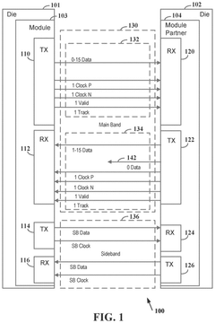
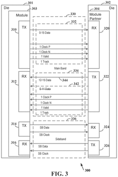
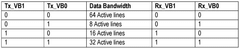
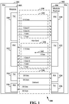
Variable link width in two directions for main band chip module connection
PatentPendingUS20240354279A1
Innovation
- Implementing a method to establish a die-to-die connection with a variable link width, allowing for independent configuration of transmit and receive data lanes through a sideband communication, enabling operation with different numbers of active data lanes in each direction to optimize power usage and data rates, and supporting fault tolerance by excluding faulty lines.
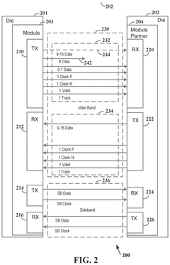
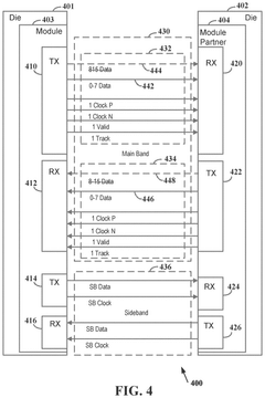
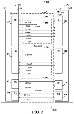
Variable link width in two directions for main band chip module connection
PatentWO2024226177A1
Innovation
- Implementing a variable link width mechanism in both directions of the main band connection, allowing for dynamic adjustment of the number of active data lanes based on requirements through a sideband communication protocol, enabling independent configuration of transmit and receive data lines to optimize power usage and data rates.

Standardization Efforts and Industry Adoption
The Universal Chiplet Interconnect Express (UCIe) has witnessed significant standardization efforts since its inception, marking a pivotal shift in the semiconductor industry's approach to chiplet-based designs. In March 2022, the UCIe Consortium was formally established with founding members including AMD, Arm, ASE, Google, Intel, Meta, Microsoft, Qualcomm, Samsung, and TSMC. This consortium represents an unprecedented collaboration among traditionally competitive entities, underscoring the industry-wide recognition of chiplet technology's importance.
The standardization process for UCIe has progressed rapidly compared to previous industry standards. Within its first year, the consortium released UCIe 1.0 specification, which defines the die-to-die interconnect between chiplets, covering both the physical layer and protocol stack. This specification enables a "plug-and-play" ecosystem where chiplets from different vendors can seamlessly integrate, significantly reducing design complexity and time-to-market.
Industry adoption of UCIe has been gaining momentum across various sectors. High-performance computing (HPC) and data center applications have been early adopters, with companies like Intel implementing UCIe in their Ponte Vecchio GPU and AMD incorporating aspects of the standard in their EPYC processors. Cloud service providers including Google and Microsoft have also signaled strong support, recognizing the potential for more customized, efficient server architectures.
The mobile and edge computing sectors are beginning to explore UCIe implementation, though adoption remains in earlier stages compared to the data center segment. Qualcomm and MediaTek have announced roadmaps that include UCIe-compatible products, potentially bringing heterogeneous integration benefits to next-generation mobile devices.
Notably, the semiconductor manufacturing ecosystem has responded positively to UCIe standardization. Advanced packaging providers like ASE, TSMC, and Samsung have developed manufacturing processes specifically optimized for UCIe-compliant chiplets. Testing and verification companies have also introduced new methodologies and equipment designed for chiplet-based architectures.
Regional adoption patterns reveal interesting dynamics, with North American and East Asian companies leading implementation efforts. European semiconductor firms have recently increased their participation, particularly in automotive and industrial applications where reliability and longevity requirements are stringent.
The UCIe Consortium continues to expand its standardization efforts, with working groups focused on advanced features including enhanced security protocols, power management specifications, and testing methodologies. The upcoming UCIe 2.0 specification is expected to address higher bandwidth requirements and improved energy efficiency metrics, further accelerating industry adoption across multiple market segments.
Thermal Management Considerations for UCIe Implementation
Thermal management represents a critical challenge in the implementation of Universal Chiplet Interconnect Express (UCIe) technology. As chiplet integration density increases, the heat generated within compact spaces creates significant thermal concerns that must be addressed through comprehensive design strategies. The thermal challenges are particularly pronounced in UCIe implementations due to the close proximity of multiple high-performance dies within a single package.
The primary thermal considerations for UCIe implementation include junction temperature management, thermal resistance optimization, and heat dissipation pathways. Junction temperatures must be maintained below critical thresholds to ensure reliable operation and prevent performance degradation. This becomes increasingly difficult as power densities rise with advanced process nodes and more complex chiplet arrangements.
Thermal interface materials (TIMs) play a crucial role in UCIe thermal management by facilitating efficient heat transfer between chiplets and heat spreaders. The selection of appropriate TIMs with optimal thermal conductivity, thickness, and reliability characteristics significantly impacts the overall thermal performance of UCIe implementations. Recent advancements in TIM technology, including metal-based and carbon-based solutions, offer promising improvements for chiplet cooling.
Active cooling solutions for UCIe packages require careful consideration of airflow patterns, heat sink designs, and potentially liquid cooling technologies for high-performance applications. The thermal design power (TDP) budget must be allocated effectively across multiple chiplets, accounting for varying workloads and potential hotspots that may develop during operation.
Thermal modeling and simulation have become essential tools in UCIe thermal management, enabling designers to predict temperature distributions and optimize cooling solutions before physical implementation. Advanced computational fluid dynamics (CFD) models can accurately simulate heat transfer across complex chiplet arrangements and package structures.
The industry is exploring innovative cooling approaches specifically tailored for chiplet architectures, including embedded microfluidic channels, phase-change materials, and direct die cooling techniques. These technologies aim to address the increasing thermal challenges as UCIe adoption expands into more demanding application domains such as high-performance computing and artificial intelligence accelerators.
Standardization efforts around thermal management for UCIe are also emerging, with industry consortia working to establish common methodologies for thermal characterization, testing, and specification. These standards will facilitate more consistent thermal design practices across the ecosystem and enable better interoperability between chiplets from different vendors.
Unlock deeper insights with Patsnap Eureka Quick Research — get a full tech report to explore trends and direct your research. Try now!
Generate Your Research Report Instantly with AI Agent
Supercharge your innovation with Patsnap Eureka AI Agent Platform!