AI Accelerator Chiplets For UCIe Chiplet Interconnect
SEP 1, 20259 MIN READ
Generate Your Research Report Instantly with AI Agent
PatSnap Eureka helps you evaluate technical feasibility & market potential.
AI Accelerator Chiplet Evolution and Objectives
AI accelerator chiplets have evolved significantly over the past decade, transitioning from monolithic designs to more modular and specialized architectures. The initial development phase focused on general-purpose GPU accelerators, which provided parallel processing capabilities but lacked AI-specific optimizations. As machine learning workloads became more prevalent, the second generation of accelerators emerged with tensor cores and specialized matrix multiplication units, dramatically improving performance for neural network computations.
The evolution accelerated with the introduction of domain-specific architectures optimized for particular AI workloads, such as inference, training, or specific neural network topologies. This specialization trend coincided with the semiconductor industry's broader shift toward chiplet-based designs to overcome the limitations of monolithic silicon scaling. The convergence of these trends has led to the current generation of AI accelerator chiplets, which combine specialized processing capabilities with modular integration potential.
The Universal Chiplet Interconnect Express (UCIe) standard represents a pivotal development in this evolution. Introduced in 2022 and backed by major industry players including Intel, AMD, Arm, and TSMC, UCIe provides a standardized die-to-die interconnect protocol that enables heterogeneous integration of chiplets from different vendors. This open ecosystem approach marks a significant departure from previous proprietary interconnect solutions.
The primary technical objectives for AI accelerator chiplets in the UCIe ecosystem include achieving near-monolithic performance while maintaining the economic and manufacturing advantages of chiplet architectures. Specifically, these objectives encompass maximizing data transfer rates between chiplets with minimal latency overhead, optimizing power efficiency for high-performance computing applications, and ensuring scalability to accommodate growing model sizes and computational demands.
Another critical objective is maintaining thermal stability across the chiplet assembly, as AI workloads typically generate significant heat that must be efficiently dissipated. Additionally, there is a strong focus on standardizing physical and logical interfaces to ensure interoperability between chiplets from different vendors, which is essential for the UCIe ecosystem to flourish.
Looking forward, the evolution trajectory aims toward increasingly specialized AI accelerator chiplets that can be mixed and matched to create custom computing solutions tailored to specific AI workloads. The ultimate goal is to establish a vibrant ecosystem where chiplet-based designs can deliver superior performance, energy efficiency, and cost-effectiveness compared to traditional monolithic approaches, while simultaneously enabling faster innovation cycles through component-level upgrades rather than complete system replacements.
Market Analysis for UCIe-based AI Accelerators
The UCIe-based AI accelerator market is experiencing rapid growth, driven by the increasing demand for high-performance computing solutions in artificial intelligence applications. Current market valuations indicate that the AI accelerator market reached approximately $21 billion in 2023, with UCIe-enabled solutions beginning to capture significant market share. Industry analysts project a compound annual growth rate of 38% for UCIe-based AI accelerators through 2028, outpacing the broader AI chip market.
The demand for UCIe-based AI accelerators stems primarily from hyperscale data centers and cloud service providers seeking to optimize their AI infrastructure. These customers require solutions that deliver superior performance per watt while maintaining flexibility in system design. The chiplet approach enabled by UCIe addresses these needs by allowing heterogeneous integration of specialized AI processing elements.
Market segmentation reveals three primary customer categories: cloud service providers (representing 65% of the market), enterprise AI deployments (25%), and edge computing applications (10%). Cloud service providers are driving adoption due to their need for customized solutions at scale, while enterprise customers are increasingly adopting UCIe-based accelerators for on-premises AI infrastructure.
Regional analysis shows North America leading adoption with 48% market share, followed by Asia-Pacific at 32%, Europe at 15%, and other regions at 5%. China's investment in domestic semiconductor capabilities is accelerating the adoption of chiplet-based designs in the Asia-Pacific region, creating a competitive landscape with North American technology leaders.
The market is characterized by strong demand elasticity, with price sensitivity varying across segments. Cloud providers prioritize performance and efficiency over initial cost, while enterprise customers demonstrate higher price sensitivity. This dynamic creates opportunities for tiered product strategies among UCIe accelerator manufacturers.
Key market drivers include the exponential growth in AI model complexity, increasing energy efficiency requirements, and the need for specialized computing architectures. The transition from monolithic designs to chiplet-based architectures is accelerating as AI workloads become more diverse, requiring different types of computing resources within the same package.
Market barriers include the technical complexity of chiplet integration, ecosystem maturity challenges, and intellectual property considerations in multi-vendor chiplet designs. Despite these challenges, the compelling economics of chiplet-based designs and the standardization provided by UCIe are overcoming adoption hesitancy.
UCIe Chiplet Interconnect: Status and Barriers
UCIe (Universal Chiplet Interconnect Express) represents a significant advancement in chiplet technology, enabling high-bandwidth, low-latency communication between different silicon dies within a package. However, despite its promising capabilities, several technical and ecosystem barriers currently limit its full potential for AI accelerator chiplets.
The primary technical challenge facing UCIe implementation is the physical integration complexity. The die-to-die interfaces require precise alignment and bonding techniques that demand advanced packaging technologies. Current manufacturing processes still struggle with yield issues when implementing the fine-pitch microbumps required for high-density interconnects, particularly at the scale needed for AI accelerator chiplets that demand massive parallel data transfer.
Power efficiency remains another significant barrier. While UCIe offers improved power characteristics compared to traditional interconnects, AI workloads require exceptional energy efficiency. The current UCIe specification still introduces power overhead that can be problematic for thermal-constrained AI accelerator designs, especially when scaling to multiple chiplets in a single package.
Bandwidth limitations also persist despite UCIe's improvements. Modern AI models continue to grow exponentially in size, requiring ever-increasing data movement capabilities. The current UCIe implementation, while offering up to 32 GT/s per lane, may still create bottlenecks for the most demanding AI training workloads that require massive parallel computing capabilities across multiple accelerator chiplets.
Protocol standardization presents another obstacle. While UCIe aims to be a universal standard, the ecosystem is still fragmented with competing interconnect technologies like NVIDIA's NVLink, AMD's Infinity Fabric, and Intel's AIB. This fragmentation complicates the development of truly interoperable chiplets from different vendors, limiting the potential for a robust multi-vendor AI accelerator chiplet ecosystem.
Testing and validation methodologies for UCIe-based systems remain underdeveloped. The complex nature of multi-chiplet designs creates challenges in isolating and diagnosing issues, particularly when integrating AI accelerator chiplets from different manufacturers. Current testing infrastructure is not fully equipped to handle the complexity of these heterogeneous systems.
Cost considerations also present barriers to widespread adoption. The advanced packaging technologies required for UCIe implementation currently command premium pricing, making UCIe-based AI accelerator solutions potentially less competitive for cost-sensitive applications. Until economies of scale drive down these costs, adoption may be limited to high-end AI systems.
Finally, software ecosystem support remains immature. Efficiently utilizing distributed AI accelerator chiplets requires sophisticated software stacks that can optimally partition and schedule workloads across multiple processing elements. Current AI frameworks and compilers are still evolving to fully leverage the potential of UCIe-connected chiplet architectures.
Current UCIe Implementation Approaches
01 Chiplet Architecture for AI Acceleration
AI accelerator chiplets employ modular architecture where multiple specialized processing units are integrated on a single package. This approach allows for optimized performance by combining different types of compute cores (like tensor processors, neural network accelerators) in a single system. The chiplet design enables better scalability, power efficiency, and customization for specific AI workloads compared to monolithic designs.- Chiplet Architecture for AI Acceleration: AI accelerator chiplets employ modular architecture where multiple specialized processing units are integrated on a single package. This approach allows for more efficient AI computation by combining different types of cores optimized for specific AI workloads. The chiplet design enables better thermal management, improved yield, and the ability to mix and match different processing elements according to specific AI application requirements.
- Interconnect Technologies for AI Chiplets: Advanced interconnect technologies are crucial for AI accelerator chiplets to achieve high-bandwidth, low-latency communication between different processing elements. These technologies include die-to-die interfaces, silicon interposers, and advanced packaging solutions that enable efficient data transfer between chiplets. The interconnect architecture significantly impacts the overall performance of AI accelerator systems by reducing communication bottlenecks between computational units.
- Memory Integration in AI Chiplets: Memory integration strategies in AI accelerator chiplets focus on reducing the data movement bottleneck that often limits AI performance. These approaches include high-bandwidth memory (HBM) stacking, on-chip memory hierarchies, and novel memory architectures specifically designed for AI workloads. By bringing memory closer to processing elements, these designs minimize latency and energy consumption associated with data movement in AI computations.
- Power Management and Thermal Solutions: AI accelerator chiplets implement sophisticated power management and thermal solutions to maximize performance within thermal constraints. These include dynamic voltage and frequency scaling, power gating for inactive components, and advanced cooling solutions specific to chiplet architectures. The modular nature of chiplets allows for more efficient thermal management by distributing heat sources across the package rather than concentrating them in a monolithic die.
- Specialized AI Processing Elements: AI accelerator chiplets incorporate specialized processing elements designed for specific AI workloads such as matrix multiplication, tensor operations, and neural network inference. These include tensor processing units, systolic arrays, and custom arithmetic units optimized for different precision formats. By tailoring hardware to specific AI algorithms, these specialized elements achieve significantly higher performance and energy efficiency compared to general-purpose processors.
02 Interconnect Technologies for AI Chiplets
Advanced interconnect technologies are crucial for AI accelerator chiplets to achieve high-bandwidth, low-latency communication between different processing elements. These technologies include die-to-die interfaces, silicon interposers, and advanced packaging solutions that enable efficient data transfer between chiplets. The interconnect architecture significantly impacts the overall performance of multi-chiplet AI accelerator systems.Expand Specific Solutions03 Memory Integration in AI Accelerator Chiplets
Memory integration strategies for AI accelerator chiplets focus on optimizing data access patterns and reducing the memory wall problem. This includes the use of high-bandwidth memory (HBM) stacks, on-chip SRAM, and novel memory hierarchies specifically designed for AI workloads. The placement and organization of memory within the chiplet architecture significantly impacts energy efficiency and computational throughput for AI applications.Expand Specific Solutions04 Power Management and Thermal Solutions for AI Chiplets
Power management and thermal solutions are essential for AI accelerator chiplets to maintain performance while operating within thermal constraints. These include dynamic voltage and frequency scaling, power gating techniques, and advanced cooling solutions specifically designed for chiplet architectures. Efficient power distribution networks and thermal management systems enable higher computational density and sustained performance in AI accelerator chiplets.Expand Specific Solutions05 Specialized AI Processing Elements in Chiplets
AI accelerator chiplets incorporate specialized processing elements optimized for specific neural network operations. These include tensor processing units, systolic arrays, and custom arithmetic units designed for matrix multiplication, convolution, and other AI-specific computations. The specialization of these processing elements allows for higher performance and energy efficiency compared to general-purpose processors when executing AI workloads.Expand Specific Solutions
Leading Companies in AI Chiplet Ecosystem
The AI accelerator chiplet market for UCIe interconnect is in its early growth phase, characterized by rapid technological innovation and strategic positioning by key players. The market is projected to expand significantly as AI workloads increase in data centers, with an estimated CAGR of 35-40% over the next five years. Major semiconductor companies including Intel, AMD (which acquired Xilinx), NVIDIA, and Qualcomm are leading development efforts, leveraging their existing chiplet expertise and UCIe founding member status. Emerging players like D-Matrix and Vastai Technologies are introducing specialized AI accelerator chiplets, while established memory manufacturers such as SK Hynix and Micron are developing complementary memory chiplet solutions. The technology is approaching commercial maturity with several companies announcing UCIe-compatible AI accelerator chiplets, though widespread deployment is expected by 2024-2025.
Intel Corp.
Technical Solution: Intel has pioneered the Universal Chiplet Interconnect Express (UCIe) standard and is leading its implementation for AI accelerator chiplets. Their approach centers on the Ponte Vecchio GPU architecture which utilizes over 40 chiplets connected via their Advanced Interface Bus (AIB) and UCIe technology. Intel's Xeon processors with integrated AI accelerator chiplets leverage UCIe to achieve high-bandwidth, low-latency die-to-die communication at 16 GT/s per pin. Their implementation includes a physical layer supporting both standard and advanced modes with bump pitches ranging from 25-55μm, a die-to-die adapter layer, and a protocol layer supporting PCIe, CXL, and other protocols. Intel's UCIe-based AI accelerator chiplets feature built-in security mechanisms, power management capabilities, and support for both package and board-level integration, enabling flexible system designs with disaggregated components[1][3].
Strengths: Industry-leading position as UCIe consortium founder with extensive IP portfolio; mature manufacturing ecosystem supporting heterogeneous integration. Weaknesses: Higher implementation complexity compared to proprietary solutions; potential interoperability challenges with third-party chiplets during early adoption phases.
QUALCOMM, Inc.
Technical Solution: Qualcomm has developed a comprehensive UCIe-compatible AI accelerator chiplet architecture optimized for mobile and edge computing applications. Their solution integrates specialized Neural Processing Units (NPUs) as discrete chiplets that connect to their Snapdragon platforms via UCIe interfaces. Qualcomm's implementation achieves up to 32 GT/s data rates with sub-picojoule-per-bit energy efficiency, critical for battery-powered devices. Their AI chiplets feature proprietary tensor acceleration units with configurable precision (INT4/INT8/FP16) and dedicated on-chiplet SRAM to minimize data movement. The architecture employs a hierarchical interconnect topology where multiple AI accelerator chiplets can be clustered and connected to a central SoC through standardized UCIe PHY and protocol layers. Qualcomm has optimized their design for heterogeneous integration, allowing AI chiplets manufactured in advanced nodes (4-5nm) to be combined with SoCs in more mature processes, balancing performance and cost[2][5].
Strengths: Industry-leading power efficiency optimized for mobile/edge deployment; mature AI software stack with extensive model optimization tools. Weaknesses: Less experience with multi-chiplet packaging compared to server-focused competitors; potentially higher unit costs due to specialized packaging requirements.
Key Patents and Research in Chiplet Interconnect
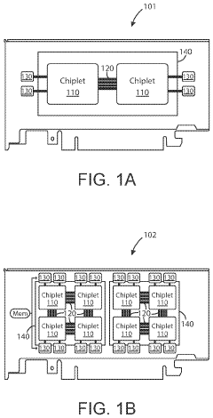
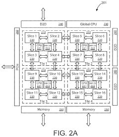
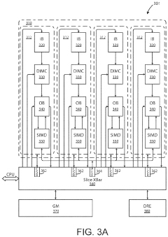
Generative ai accelerator apparatus using in-memory compute chiplet devices for transformer workloads
PatentActiveUS20230168899A1
Innovation
- The implementation of AI accelerator apparatuses using chiplet devices with digital in-memory compute functionality, which includes multiple slices with CPUs and hardware dispatch devices, along with die-to-die interconnects and PCIe buses, to accelerate transformer computations by integrating computational functions and memory fabric, enabling efficient processing and reducing power consumption.
Semiconductor device based on UCIe interface
PatentActiveCN117222234A
Innovation
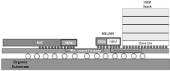
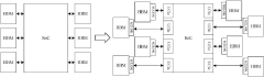
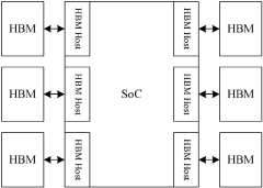
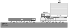
- Using semiconductor devices based on the UCIe interface, the SoC is decoupled from the HBM through joint dies, and the rewiring layer and organic substrate are used for interconnection, avoiding the silicon interposer, realizing the decoupling of the SoC and HBM memory, and through the on-chip bus Perform data exchange.
Thermal Management Challenges and Solutions
The integration of AI accelerator chiplets with UCIe interconnect technology introduces significant thermal management challenges that must be addressed for optimal system performance. As chiplet-based designs become more prevalent in high-performance computing applications, the thermal density increases dramatically, particularly in AI accelerators where computational intensity is exceptionally high. These chiplets can generate heat fluxes exceeding 500W/cm², creating hotspots that threaten system reliability and performance.
UCIe interconnect technology compounds these challenges through its high-density packaging approach. The reduced spacing between chiplets limits thermal dissipation pathways and creates thermal coupling effects where heat from one chiplet affects adjacent components. This is particularly problematic in heterogeneous integration scenarios where AI accelerators are combined with memory, I/O, and other functional chiplets with different thermal characteristics and tolerances.
Advanced cooling solutions are emerging to address these thermal challenges. Liquid cooling technologies, including direct-to-chip liquid cooling and immersion cooling, offer superior thermal conductivity compared to traditional air cooling. These solutions can manage the extreme heat loads generated by AI accelerator chiplets while maintaining junction temperatures within acceptable operating ranges. Microfluidic cooling channels integrated directly into the interposer or package substrate represent another promising approach, enabling targeted cooling of hotspots.
Thermal interface materials (TIMs) play a crucial role in chiplet-based designs. Next-generation TIMs with thermal conductivities exceeding 25 W/m·K are being developed specifically for chiplet applications, including phase-change materials, metal-based TIMs, and carbon nanotube arrays that provide superior thermal transfer between chiplets and heat spreaders.
Dynamic thermal management strategies are increasingly important for AI accelerator chiplets. Advanced techniques include predictive thermal modeling, workload-aware power management, and thermal-aware task scheduling that dynamically adjusts computational loads across chiplets to prevent thermal emergencies. These approaches are complemented by hardware-level thermal sensors embedded within the chiplets that enable real-time temperature monitoring and response.
The industry is also exploring novel package-level solutions such as integrated vapor chambers, graphene-based heat spreaders, and diamond-copper composite materials that offer exceptional thermal conductivity. These materials help distribute heat more effectively across the package, reducing thermal gradients and hotspots that can impact UCIe link performance and reliability.
Standardization Efforts in Chiplet Interfaces
The standardization of chiplet interfaces represents a critical evolution in semiconductor integration, particularly for AI accelerator chiplets utilizing UCIe (Universal Chiplet Interconnect Express). This standardization effort has gained significant momentum as the industry recognizes the need for common protocols to enable multi-vendor chiplet ecosystems.
UCIe emerged as a leading standard in 2022 when industry giants including Intel, AMD, Arm, TSMC, Samsung, and Google formed the UCIe consortium. The standard defines both the physical layer and protocol stack for die-to-die interconnection, supporting different packaging technologies while ensuring interoperability across vendors. For AI accelerators, this standardization is particularly valuable as it enables specialized AI processing elements to be integrated with other system components efficiently.
The standardization process has evolved through several key phases. Initially, the focus was on establishing physical layer specifications, addressing signal integrity, power delivery, and thermal considerations. Subsequently, attention shifted to protocol standardization, ensuring efficient data movement between chiplets with minimal latency and maximum bandwidth - critical requirements for AI workloads.
Current UCIe specifications define multiple interface modes, including an ultra-short-reach (USR) PHY for die-to-die connections and a standard PHY for package-to-package links. The standard supports both advanced packaging technologies like silicon interposers and more conventional organic substrates, providing flexibility for different AI accelerator implementations.
Beyond UCIe, complementary standards are emerging to address specific aspects of chiplet integration. The Open Compute Project's Bunch of Wires (BoW) specification offers a simpler alternative for certain applications, while JEDEC's standards address memory interfaces critical for AI accelerator performance. The Compute Express Link (CXL) consortium is working to ensure compatibility between its cache coherency protocols and UCIe, which is essential for complex AI systems.
Industry adoption metrics indicate accelerating implementation of these standards, with major AI chip developers incorporating UCIe-compatible interfaces into their latest designs. The standardization timeline projects complete ecosystem maturity by 2025-2026, when fully interoperable multi-vendor AI chiplet solutions are expected to reach production volumes.
Challenges remain in standardizing test methodologies, security protocols, and power management interfaces specific to AI accelerator requirements. Working groups within the UCIe consortium are actively addressing these gaps to ensure comprehensive coverage of all aspects needed for successful AI chiplet integration.
Unlock deeper insights with PatSnap Eureka Quick Research — get a full tech report to explore trends and direct your research. Try now!
Generate Your Research Report Instantly with AI Agent
Supercharge your innovation with PatSnap Eureka AI Agent Platform!