

UCIe Chiplet Interconnect Packaging EDA Integration Solutions
SEP 1, 20259 MIN READ
Generate Your Research Report Instantly with AI Agent
Patsnap Eureka helps you evaluate technical feasibility & market potential.
UCIe Chiplet Technology Evolution and Objectives
Universal Chiplet Interconnect Express (UCIe) represents a significant evolution in semiconductor integration technology, emerging from the limitations of traditional monolithic chip designs. The technology's development can be traced back to the early 2010s when the semiconductor industry began exploring chiplet-based architectures to address scaling challenges in Moore's Law. UCIe specifically evolved from earlier proprietary interconnect technologies, with its formal introduction as an open industry standard in March 2022 by a consortium of leading semiconductor companies including Intel, AMD, Arm, and TSMC.
The evolution of UCIe technology has been driven by several key factors: the increasing complexity and cost of monolithic chip manufacturing at advanced nodes, the need for heterogeneous integration of different process technologies, and the demand for more flexible and scalable system designs. This evolution represents a paradigm shift from System-on-Chip (SoC) to System-in-Package (SiP) architectures, enabling the integration of multiple specialized chiplets within a single package.
UCIe's technical evolution encompasses both die-to-die (D2D) and package-to-package (P2P) interconnect technologies, with standardized protocols for physical layer, die-to-die adapter, and protocol layers. The standard has progressed through version 1.0 and subsequent iterations, each enhancing bandwidth, reducing latency, and improving power efficiency of chiplet communications.
The primary objectives of UCIe technology development include establishing an open, unified interconnect standard to ensure interoperability between chiplets from different vendors, enabling a more diverse and competitive chiplet ecosystem. Technical objectives focus on achieving high-bandwidth, low-latency connections between chiplets while maintaining power efficiency and signal integrity across different packaging technologies.
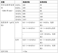
Performance targets for UCIe include data rates exceeding 16 GT/s in its initial specification, with roadmaps targeting 32 GT/s and beyond in future iterations. The standard aims to support both advanced packaging technologies like silicon interposers and more cost-effective organic substrate approaches, providing flexibility across different market segments and applications.
Long-term objectives for UCIe technology include enabling a true "chiplet marketplace" where standardized components from multiple vendors can be seamlessly integrated, reducing development costs and time-to-market for complex semiconductor products. This vision requires not only technical standardization but also the development of comprehensive design, verification, and testing methodologies supported by advanced EDA tools and manufacturing processes.
The evolution of UCIe technology has been driven by several key factors: the increasing complexity and cost of monolithic chip manufacturing at advanced nodes, the need for heterogeneous integration of different process technologies, and the demand for more flexible and scalable system designs. This evolution represents a paradigm shift from System-on-Chip (SoC) to System-in-Package (SiP) architectures, enabling the integration of multiple specialized chiplets within a single package.
UCIe's technical evolution encompasses both die-to-die (D2D) and package-to-package (P2P) interconnect technologies, with standardized protocols for physical layer, die-to-die adapter, and protocol layers. The standard has progressed through version 1.0 and subsequent iterations, each enhancing bandwidth, reducing latency, and improving power efficiency of chiplet communications.
The primary objectives of UCIe technology development include establishing an open, unified interconnect standard to ensure interoperability between chiplets from different vendors, enabling a more diverse and competitive chiplet ecosystem. Technical objectives focus on achieving high-bandwidth, low-latency connections between chiplets while maintaining power efficiency and signal integrity across different packaging technologies.
Performance targets for UCIe include data rates exceeding 16 GT/s in its initial specification, with roadmaps targeting 32 GT/s and beyond in future iterations. The standard aims to support both advanced packaging technologies like silicon interposers and more cost-effective organic substrate approaches, providing flexibility across different market segments and applications.
Long-term objectives for UCIe technology include enabling a true "chiplet marketplace" where standardized components from multiple vendors can be seamlessly integrated, reducing development costs and time-to-market for complex semiconductor products. This vision requires not only technical standardization but also the development of comprehensive design, verification, and testing methodologies supported by advanced EDA tools and manufacturing processes.
Market Demand Analysis for Chiplet Integration Solutions
The global chiplet market is experiencing unprecedented growth, driven by the increasing demand for high-performance computing solutions across various industries. As traditional monolithic chip designs reach their physical and economic limits, chiplet-based architectures have emerged as a compelling alternative. Market research indicates that the chiplet market is projected to grow at a compound annual growth rate of 38% from 2023 to 2030, reaching approximately 57 billion USD by the end of the forecast period.
The primary market drivers for UCIe chiplet interconnect packaging and EDA integration solutions stem from several converging factors. Data centers and cloud service providers are seeking more efficient computing architectures to handle exponentially growing workloads while managing power consumption and thermal constraints. The artificial intelligence and machine learning sectors require specialized accelerators that can be rapidly developed and deployed, making modular chiplet designs particularly attractive.
Consumer electronics manufacturers are also showing increased interest in chiplet technology as they strive to deliver more powerful devices with longer battery life and smaller form factors. The automotive industry represents another significant market segment, with advanced driver assistance systems and autonomous driving capabilities demanding high-performance, reliable computing platforms that can be customized for specific applications.
From a geographical perspective, North America currently leads the chiplet market, accounting for approximately 42% of global demand, followed by Asia-Pacific at 38% and Europe at 15%. However, the Asia-Pacific region is expected to show the fastest growth rate over the next five years due to increasing semiconductor manufacturing capabilities and government initiatives supporting advanced chip technologies.
The market demand for UCIe-based solutions specifically has intensified following the establishment of the UCIe consortium in 2022. Industry surveys indicate that 78% of semiconductor companies are either actively developing or planning to develop UCIe-compliant products within the next three years. This standardization effort has created a significant opportunity for EDA tool providers to develop integrated solutions that address the unique challenges of chiplet-based designs.
Customer requirements analysis reveals several key demands driving the market: seamless integration between different vendors' chiplets, reduced design cycle time, improved power efficiency, enhanced thermal management capabilities, and comprehensive testing methodologies for multi-die packages. Additionally, there is growing demand for EDA tools that can effectively model and simulate the complex interactions between chiplets from different process nodes and manufacturers.
UCIe Interconnect Technical Challenges and Standards
The UCIe (Universal Chiplet Interconnect Express) standard represents a significant advancement in chiplet-based design methodology, addressing the growing need for modular chip architectures. As Moore's Law faces physical limitations, the industry has pivoted toward chiplet technology to maintain performance scaling while managing manufacturing costs and yield challenges.
UCIe faces several critical technical challenges that must be overcome for widespread adoption. The primary challenge lies in achieving high-bandwidth, low-latency communication between chiplets while maintaining power efficiency. Current implementations struggle to balance these competing requirements, particularly as data rates exceed 16 GT/s. Signal integrity issues become pronounced at these speeds, requiring sophisticated equalization techniques and careful channel design.
Another significant challenge is thermal management across the chiplet ecosystem. The dense integration of multiple dies creates concentrated heat zones that can lead to performance throttling and reliability concerns. Traditional cooling solutions often prove inadequate for these complex thermal profiles, necessitating innovative approaches to heat dissipation.
The standard must also address testing complexities unique to multi-die packages. Known-good-die testing becomes essential but presents methodological challenges when chiplets are designed to function interdependently. This creates a verification gap that current testing infrastructures struggle to bridge effectively.
Power delivery represents another formidable challenge, as voltage drops across interconnects can create performance inconsistencies between chiplets. The standard must define robust power delivery network specifications that ensure stable operation across all integrated components.
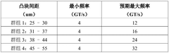
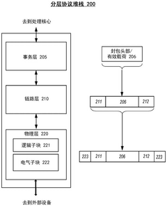
The UCIe standard aims to address these challenges through a comprehensive specification that defines both physical and protocol layers. At the physical layer, it establishes parameters for die-to-die interfaces, including bump pitches, channel characteristics, and electrical specifications. The standard supports both standard and advanced packaging technologies, accommodating both silicon interposer and organic substrate implementations.
At the protocol layer, UCIe defines transaction protocols, flow control mechanisms, and error handling procedures. It establishes a flexible architecture that supports various communication models, from simple load/store operations to more complex coherent transactions. This flexibility allows chiplet designers to optimize for specific application requirements while maintaining interoperability.
The standard's development has been driven by a consortium of industry leaders, ensuring broad compatibility across the semiconductor ecosystem. Its phased approach to implementation allows for incremental adoption, with initial focus on establishing fundamental interoperability before addressing more advanced features in subsequent revisions.
UCIe faces several critical technical challenges that must be overcome for widespread adoption. The primary challenge lies in achieving high-bandwidth, low-latency communication between chiplets while maintaining power efficiency. Current implementations struggle to balance these competing requirements, particularly as data rates exceed 16 GT/s. Signal integrity issues become pronounced at these speeds, requiring sophisticated equalization techniques and careful channel design.
Another significant challenge is thermal management across the chiplet ecosystem. The dense integration of multiple dies creates concentrated heat zones that can lead to performance throttling and reliability concerns. Traditional cooling solutions often prove inadequate for these complex thermal profiles, necessitating innovative approaches to heat dissipation.
The standard must also address testing complexities unique to multi-die packages. Known-good-die testing becomes essential but presents methodological challenges when chiplets are designed to function interdependently. This creates a verification gap that current testing infrastructures struggle to bridge effectively.
Power delivery represents another formidable challenge, as voltage drops across interconnects can create performance inconsistencies between chiplets. The standard must define robust power delivery network specifications that ensure stable operation across all integrated components.
The UCIe standard aims to address these challenges through a comprehensive specification that defines both physical and protocol layers. At the physical layer, it establishes parameters for die-to-die interfaces, including bump pitches, channel characteristics, and electrical specifications. The standard supports both standard and advanced packaging technologies, accommodating both silicon interposer and organic substrate implementations.
At the protocol layer, UCIe defines transaction protocols, flow control mechanisms, and error handling procedures. It establishes a flexible architecture that supports various communication models, from simple load/store operations to more complex coherent transactions. This flexibility allows chiplet designers to optimize for specific application requirements while maintaining interoperability.
The standard's development has been driven by a consortium of industry leaders, ensuring broad compatibility across the semiconductor ecosystem. Its phased approach to implementation allows for incremental adoption, with initial focus on establishing fundamental interoperability before addressing more advanced features in subsequent revisions.
Current EDA Solutions for Chiplet Integration
01 UCIe architecture and protocol specifications
Universal Chiplet Interconnect Express (UCIe) defines standardized architecture and protocols for chiplet-to-chiplet communication. This includes specifications for physical layer connectivity, data transfer protocols, and signal integrity requirements that enable high-bandwidth, low-latency communication between different chiplets in a package. The architecture supports various die-to-die interconnect technologies while maintaining compatibility across different manufacturers' components.- UCIe architecture and protocol specifications: Universal Chiplet Interconnect Express (UCIe) defines a standardized architecture and protocol for connecting different chiplets within a package. The specifications include physical layer requirements, protocol stack, and electrical interfaces that enable high-speed, low-latency communication between chiplets. This standardization allows for interoperability between chiplets from different manufacturers, supporting modular chip design approaches while maintaining high performance interconnections.
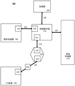
- Integration of heterogeneous chiplets using UCIe: UCIe technology enables the integration of heterogeneous chiplets manufactured using different process technologies or from different vendors. This approach allows system designers to combine specialized chiplets (such as CPUs, GPUs, memory, and accelerators) into a single package, optimizing performance, power efficiency, and cost. The UCIe standard provides the necessary interconnect framework to ensure these diverse components can communicate effectively while maintaining signal integrity across the package.
- Power management and thermal considerations in UCIe implementations: UCIe implementations incorporate advanced power management techniques to optimize energy efficiency in multi-chiplet packages. These include dynamic voltage and frequency scaling, power state management, and thermal monitoring across chiplet boundaries. The standard supports mechanisms for coordinated power management between chiplets, allowing for efficient operation while maintaining thermal constraints in densely packed chiplet configurations.
- Testing and validation methodologies for UCIe interfaces: Specialized testing and validation methodologies have been developed for UCIe interfaces to ensure reliability and performance. These include built-in self-test mechanisms, boundary scan techniques, and specialized test patterns designed to verify signal integrity across chiplet boundaries. The testing approaches address unique challenges in multi-chiplet packages, including die-to-die connections, ensuring manufacturability and long-term reliability of UCIe-based systems.
- Packaging technologies supporting UCIe implementation: Advanced packaging technologies are essential for implementing UCIe-based chiplet designs. These include silicon interposers, organic substrates, and advanced 2.5D/3D integration techniques that provide the physical foundation for chiplet-to-chiplet connections. The packaging solutions address challenges such as signal routing density, mechanical stability, and thermal dissipation while enabling the high-bandwidth, low-latency connections required by the UCIe standard.
02 Integration of heterogeneous chiplets using UCIe
UCIe enables the integration of heterogeneous chiplets manufactured using different process technologies or from different vendors. This approach allows system designers to combine specialized chiplets (such as CPUs, GPUs, memory, and accelerators) into a single package while maintaining standardized interfaces between them. The technology supports both 2D and 3D integration methods, providing flexibility in package design while ensuring interoperability between components.Expand Specific Solutions03 Power management and thermal considerations in UCIe implementations
UCIe implementations incorporate advanced power management techniques to optimize energy efficiency across interconnected chiplets. This includes dynamic power scaling, sleep states, and localized power domains that can be independently controlled. Thermal management solutions are also integrated to address heat dissipation challenges in densely packed chiplet configurations, ensuring reliable operation under various workloads while maintaining signal integrity across the interconnects.Expand Specific Solutions04 Testing and validation methodologies for UCIe interfaces
Specialized testing and validation methodologies have been developed for UCIe interfaces to ensure proper functionality and compliance with the standard. These include built-in self-test mechanisms, boundary scan techniques, and loopback testing capabilities that can verify signal integrity, timing parameters, and protocol compliance. Advanced debug features allow for monitoring and diagnosing interconnect issues during development and in field deployments.Expand Specific Solutions05 Security features and encryption in UCIe communication
UCIe implementations incorporate security features to protect data exchanged between chiplets. This includes authentication mechanisms to verify the identity of connected chiplets, encryption capabilities to secure sensitive data during transmission, and secure boot processes to ensure system integrity. Hardware-based security features are integrated into the interconnect fabric to prevent unauthorized access or tampering while maintaining the performance requirements of high-speed chiplet communication.Expand Specific Solutions
Key Industry Players in UCIe Ecosystem
The UCIe Chiplet Interconnect Packaging EDA Integration Solutions market is currently in an early growth phase, characterized by rapid technological development and increasing industry adoption. The market is projected to expand significantly as heterogeneous integration becomes essential for advanced computing systems. Intel leads the ecosystem as a founding member of the UCIe consortium, with TSMC, Samsung, and GLOBALFOUNDRIES representing key foundry players. Qualcomm, AMD (formerly Xilinx), and Huawei are advancing chiplet designs while Cadence provides critical EDA tools. The technology is approaching maturity for high-performance computing applications but remains in development for broader market segments, with newer entrants like Chipletz and Jariet Technologies introducing specialized solutions for chiplet-based designs.
Intel Corp.
Technical Solution: Intel has pioneered UCIe (Universal Chiplet Interconnect Express) as a founding member of the UCIe Consortium. Their technology solution centers on the Advanced Interface Bus (AIB) which serves as the foundation for UCIe. Intel's approach includes a comprehensive chiplet ecosystem with their Embedded Multi-die Interconnect Bridge (EMIB) packaging technology that enables high-bandwidth, low-power connections between chiplets. Intel's Ponte Vecchio GPU demonstrates their UCIe implementation, featuring over 100 billion transistors across 47 chiplets using EMIB and Foveros packaging technologies. Their EDA integration solution includes collaboration with major EDA vendors to develop design tools specifically for UCIe-based chiplet designs, supporting physical design verification, signal integrity analysis, and thermal modeling for multi-chiplet packages[1][3].
Strengths: Industry-leading position as UCIe founder with proven implementation in products like Ponte Vecchio; extensive IP portfolio and manufacturing capabilities for chiplet integration. Weaknesses: Proprietary aspects of their implementation may limit broader ecosystem adoption; complex integration requirements may increase design costs and time-to-market.
QUALCOMM, Inc.
Technical Solution: Qualcomm has developed a comprehensive UCIe-based chiplet integration solution focused on mobile and edge computing applications. Their approach leverages their expertise in system-on-chip design to create a modular chiplet architecture that maintains high performance while reducing power consumption. Qualcomm's solution includes a proprietary die-to-die (D2D) interface that is UCIe-compliant, allowing for high-bandwidth, low-latency connections between heterogeneous chiplets. Their EDA integration framework provides tools for chiplet-based SoC design, including automated partitioning optimization, interface synthesis, and verification methodologies specific to multi-die systems. Qualcomm has implemented advanced thermal management techniques to address the unique challenges of chiplet designs in thermally constrained mobile devices[2][5].
Strengths: Strong expertise in low-power, high-performance mobile chipsets; established manufacturing partnerships for advanced packaging. Weaknesses: Less public disclosure of specific UCIe implementations compared to competitors; primarily focused on mobile applications rather than broader computing markets.
Critical IP and Design Methodologies for UCIe
Die-to-die interconnect
PatentPendingCN117651940A
Innovation
- Using the Universal Chiplet Interconnect Express (UCIe) protocol, this protocol provides a universal, open on-package interconnect standard that supports high bandwidth, low latency and high power efficiency inter-core connections through standardized dies to The die interface enables interoperability across suppliers and factories.
Electronic device
PatentPendingUS20240371781A1
Innovation
- The electronic device employs a substrate with an interconnect structure that includes misaligned via structures composed of fewer stacked vias, reducing fabrication complexity and cost, and is designed to ensure SI/PI performance by using additional signal traces and ground layers to improve signal and power integrity at deeper levels of the substrate.
Thermal Management Strategies for Multi-Chiplet Systems
Thermal management has emerged as a critical challenge in multi-chiplet systems utilizing UCIe (Universal Chiplet Interconnect Express) technology. As chiplet designs become more prevalent in high-performance computing applications, the increased power density and heat generation within compact packaging create significant thermal constraints that must be addressed through innovative solutions.
Current thermal management approaches for UCIe-based systems employ a multi-layered strategy. At the die level, designers are implementing advanced power gating techniques and dynamic voltage frequency scaling (DVFS) to reduce heat generation at the source. These techniques are being integrated directly into the chiplet design process through specialized EDA tools that can model thermal characteristics during the early design phases.
The interface between chiplets represents a particular thermal challenge in UCIe implementations. Thermal interface materials (TIMs) with enhanced thermal conductivity are being developed specifically for chiplet-to-chiplet and chiplet-to-substrate connections. These advanced TIMs achieve thermal conductivity values exceeding 20 W/m·K while maintaining the mechanical properties required for reliable interconnects.
Package-level thermal solutions for multi-chiplet systems have evolved beyond traditional heatsinks. Vapor chambers and micro-channel liquid cooling solutions are being customized for the unique thermal profiles of UCIe packages. These solutions can address hotspots that occur at chiplet interfaces and high-density computing elements. EDA tools now incorporate computational fluid dynamics (CFD) capabilities to simulate these cooling mechanisms during the design phase.
System-level thermal management for UCIe implementations increasingly relies on AI-driven predictive thermal modeling. These models can anticipate thermal emergencies before they occur and trigger appropriate mitigation strategies. The integration of these thermal management systems with EDA tools allows for comprehensive thermal verification throughout the design process.
Emerging research focuses on heterogeneous integration of thermal management directly into the chiplet architecture. This includes embedded micro-fluidic channels within the interposer and thermally-aware placement of chiplets based on their power profiles. Advanced EDA tools now support these design methodologies through specialized thermal analysis modules that can simulate the complex heat transfer mechanisms in multi-chiplet packages.
The industry is moving toward standardized thermal models for UCIe implementations to facilitate interoperability between different vendors' chiplets. These standardized models are being incorporated into EDA platforms to ensure thermal compatibility across heterogeneous chiplet designs from different manufacturers, further enhancing the UCIe ecosystem's viability for complex computing applications.
Supply Chain Considerations for Chiplet Manufacturing
The chiplet manufacturing ecosystem presents unique supply chain challenges that differ significantly from traditional monolithic chip production. The disaggregation of system functionality across multiple dies necessitates a more complex and coordinated supply chain network. For UCIe-based chiplet solutions, manufacturers must establish robust relationships with multiple suppliers specializing in different aspects of the chiplet ecosystem, including die fabrication, advanced packaging, testing, and assembly.
Material sourcing becomes particularly critical in chiplet manufacturing, as the integration of heterogeneous dies requires compatible materials that can withstand the thermal and mechanical stresses of advanced packaging processes. The availability of specialized substrate materials, interposers, and micro-bumping materials directly impacts production capabilities and yield rates. Companies implementing UCIe solutions must develop strategic partnerships with material suppliers to ensure consistent quality and availability.
Geographical distribution of the chiplet supply chain introduces additional complexities. While front-end fabrication remains concentrated in East Asia, advanced packaging capabilities are more distributed globally. This geographical dispersion necessitates sophisticated logistics management to coordinate the movement of dies between facilities while maintaining the stringent cleanliness and handling requirements essential for high-yield assembly.
Inventory management strategies for chiplet manufacturing differ substantially from traditional semiconductor approaches. The modular nature of chiplets allows for more flexible production planning but requires precise coordination across multiple die types. Companies must balance the benefits of standardization against the need for customization, developing inventory strategies that accommodate both high-volume standard chiplets and specialized application-specific dies.
Testing and quality assurance present unique supply chain challenges in the chiplet ecosystem. Known-good-die (KGD) testing becomes essential before integration, as defects in individual chiplets can compromise entire multi-die packages. This necessitates specialized testing equipment and expertise distributed throughout the supply chain, with clear protocols for defect identification and traceability.
Regulatory compliance and intellectual property protection add another layer of complexity to chiplet supply chains. As dies move between different facilities and potentially across international borders, maintaining consistent compliance with export controls and protecting proprietary designs becomes increasingly challenging. Companies implementing UCIe solutions must develop comprehensive frameworks for managing these risks across their extended supply networks.
Unlock deeper insights with Patsnap Eureka Quick Research — get a full tech report to explore trends and direct your research. Try now!
Generate Your Research Report Instantly with AI Agent
Supercharge your innovation with Patsnap Eureka AI Agent Platform!