Die-To-Die Latency Budget In UCIe Chiplet Interconnect
SEP 1, 20259 MIN READ
Generate Your Research Report Instantly with AI Agent
Patsnap Eureka helps you evaluate technical feasibility & market potential.
UCIe Chiplet Interconnect Background and Objectives
The Universal Chiplet Interconnect Express (UCIe) represents a significant advancement in semiconductor integration technology, emerging as a response to the increasing challenges of traditional monolithic chip scaling. As Moore's Law faces physical and economic limitations, the industry has pivoted toward chiplet-based architectures, where multiple smaller dies are integrated into a single package. UCIe was established in 2022 by a consortium of leading semiconductor companies including Intel, AMD, Arm, and TSMC, with the goal of creating an open industry standard for die-to-die interconnects.
The evolution of chiplet technology can be traced back to the early 2010s, when companies began exploring multi-chip module approaches. However, the lack of standardization created significant interoperability challenges. UCIe addresses this by providing a unified framework for chiplet communication, enabling dies from different manufacturers to work seamlessly together within the same package.
UCIe's technical objectives focus on establishing a comprehensive specification that covers both the physical layer and protocol stack for die-to-die communication. The standard aims to support multiple packaging technologies, including both 2D and 3D integration methods, while maintaining backward compatibility to protect industry investments.
A primary goal of UCIe is to optimize the latency budget for die-to-die communication, which is critical for maintaining system performance in disaggregated architectures. The standard targets latencies in the single-digit nanosecond range, significantly lower than traditional off-chip communication methods. This aggressive latency target is essential for enabling high-performance computing applications where chiplets must communicate as efficiently as if they were on the same die.
The UCIe specification encompasses multiple data rate options, from 16 GT/s in its initial version to a roadmap extending to 32 GT/s and beyond. These increasing data rates are designed to support the growing bandwidth demands of next-generation computing systems, particularly in data centers, AI acceleration, and high-performance computing environments.
Energy efficiency represents another crucial objective for UCIe, with targets of less than 1 pJ/bit for die-to-die communication. This efficiency is vital for managing thermal constraints in densely packed chiplet designs and supporting the industry's sustainability goals.
Looking forward, UCIe aims to establish an ecosystem that fosters innovation through specialized chiplets while maintaining interoperability. The standard is expected to evolve to support emerging technologies such as optical interconnects and advanced packaging techniques, ensuring its relevance as the semiconductor industry continues to transform.
Market Demand Analysis for Die-to-Die Interconnect Solutions
The demand for die-to-die interconnect solutions has witnessed exponential growth in recent years, primarily driven by the semiconductor industry's shift towards chiplet-based architectures. This transition is necessitated by the slowing of Moore's Law and the increasing challenges in traditional monolithic chip scaling. Market research indicates that the chiplet market is projected to grow at a CAGR of 40% from 2023 to 2028, with die-to-die interconnect technologies being a critical enabler of this growth.
The UCIe (Universal Chiplet Interconnect Express) standard, introduced in 2022, has emerged as a pivotal technology addressing the industry's need for standardized die-to-die communication. The market demand for UCIe-compliant solutions is particularly strong in high-performance computing, data centers, and AI/ML applications where system performance is increasingly bottlenecked by interconnect capabilities rather than computational resources.
Latency requirements in these markets are becoming increasingly stringent. Data center operators report that even microsecond-level improvements in communication latency can translate to significant competitive advantages in applications like high-frequency trading, real-time analytics, and AI inference. This has created a premium market segment for ultra-low-latency die-to-die interconnect solutions.
The automotive and industrial sectors are also emerging as significant markets for chiplet technologies, with requirements focusing on reliability and deterministic latency rather than absolute performance. These sectors value predictable performance characteristics that can be guaranteed across varying environmental conditions.
Consumer electronics manufacturers are exploring chiplet designs to enable more customizable and power-efficient devices. In this market segment, the balance between latency, power consumption, and cost is particularly critical, with manufacturers willing to accept slightly higher latencies if power efficiency benefits are substantial.
From a geographical perspective, North America and East Asia dominate the demand for advanced die-to-die interconnect solutions, with major cloud service providers and semiconductor companies driving innovation. Europe shows growing interest, particularly in automotive and industrial applications of chiplet technology.
The market is also witnessing increased demand for testing and validation tools specific to die-to-die interconnects, as manufacturers seek to characterize and optimize latency budgets in their designs. This has created a parallel market for specialized test equipment and simulation software capable of accurately modeling multi-die systems.
Overall, the market trajectory clearly indicates that optimizing die-to-die latency budgets in UCIe and similar interconnect technologies will remain a critical competitive differentiator for semiconductor companies in the coming years, with particular emphasis on standardization, power efficiency, and application-specific optimization.
Current State and Challenges in Die-to-Die Latency Management
The current state of die-to-die latency management in UCIe chiplet interconnect technology presents both significant advancements and persistent challenges. UCIe (Universal Chiplet Interconnect Express) has emerged as a promising standard for chiplet integration, with latency being one of the critical performance metrics. Current implementations achieve latencies ranging from 2-20ns depending on the specific implementation, package technology, and communication protocol used.
Industry leaders including Intel, AMD, TSMC, and Samsung have made substantial progress in reducing die-to-die latency through advanced packaging technologies such as EMIB (Embedded Multi-die Interconnect Bridge) and CoWoS (Chip-on-Wafer-on-Substrate). These approaches have demonstrated latency improvements of up to 40% compared to traditional interposer-based solutions.
The primary technical challenges currently facing die-to-die latency management include signal integrity issues at high frequencies, power delivery constraints, thermal management concerns, and clock domain crossing complexities. Signal integrity degradation can add 0.5-2ns of additional latency due to increased jitter and noise at high data rates exceeding 16GT/s.
Physical distance between dies remains a fundamental limiting factor, with each millimeter of trace length adding approximately 5-7ps of latency. This physical constraint becomes particularly problematic in complex multi-chiplet designs where optimal placement is restricted by thermal and power considerations.
Protocol overhead represents another significant challenge, with current UCIe implementations allocating 15-30% of the total latency budget to protocol processing. This includes time spent on error detection and correction, flow control mechanisms, and addressing schemes. While necessary for reliable communication, these protocol layers add substantial latency that cannot be easily reduced without compromising system reliability.
Clock domain synchronization between different chiplets introduces additional latency penalties of 1-3ns depending on the synchronization mechanism employed. Asynchronous crossing techniques reduce this penalty but increase design complexity and verification challenges.
Manufacturing variability presents another obstacle, with process variations causing latency differences of up to 15% between identical designs. This variability complicates timing closure and necessitates conservative design margins that further impact overall performance.
The industry is currently exploring several promising approaches to address these challenges, including advanced equalization techniques, reduced-swing signaling, and novel clocking architectures. Additionally, co-design methodologies that simultaneously optimize physical layout, electrical parameters, and protocol implementations are showing potential for holistic latency improvements of 20-30% in next-generation designs.
Current Latency Budget Allocation Methodologies in UCIe
01 Latency reduction techniques in UCIe chiplet interconnects
Various techniques are employed to reduce latency in UCIe chiplet interconnects, including optimized routing algorithms, advanced buffering mechanisms, and specialized circuit designs. These approaches minimize signal propagation delays between chiplets, enabling faster data transfer and improved overall system performance. The implementation of these techniques allows for more efficient communication between different functional blocks in multi-chiplet architectures.- Latency reduction techniques in UCIe chiplet interconnects: Various techniques are employed to reduce latency in UCIe chiplet interconnects, including optimized routing algorithms, advanced buffering mechanisms, and specialized circuit designs. These approaches minimize signal propagation delays between chiplets, enabling faster data transfer and improved overall system performance. The implementation of these techniques allows for more efficient communication between different functional blocks within a multi-chiplet architecture.
- Die-to-die communication protocols for UCIe: Specific communication protocols are developed for die-to-die interfaces in UCIe implementations to optimize latency. These protocols include specialized handshaking mechanisms, efficient packet structures, and optimized flow control methods. By implementing these protocols, chiplet-based systems can achieve lower communication overhead and reduced latency between different dies, resulting in improved system responsiveness and throughput.
- Physical layer optimizations for UCIe latency: The physical layer of UCIe interconnects is optimized through various techniques to minimize latency, including advanced signaling methods, improved channel designs, and enhanced clock distribution networks. These optimizations focus on reducing signal propagation time and improving signal integrity across the interconnect. By enhancing the physical layer characteristics, UCIe implementations can achieve lower latency while maintaining reliable data transmission between chiplets.
- Architecture-level approaches for latency management: Architecture-level strategies are employed to manage latency in UCIe chiplet interconnects, including optimized topology designs, strategic placement of chiplets, and efficient resource allocation. These approaches consider the overall system architecture to minimize communication distances and reduce contention points. By implementing these architectural optimizations, UCIe-based systems can achieve lower end-to-end latency and improved performance for complex multi-chiplet designs.
- Advanced power management for latency optimization: Power management techniques are implemented in UCIe chiplet interconnects to optimize latency while maintaining energy efficiency. These include dynamic voltage and frequency scaling, selective power gating, and adaptive power allocation based on communication demands. By balancing power consumption with performance requirements, these techniques enable UCIe implementations to achieve low latency communication while minimizing energy usage, which is particularly important for high-performance computing applications.
02 Die-to-die communication protocols for UCIe
Specific communication protocols are developed for die-to-die connections in UCIe implementations to optimize latency. These protocols include specialized handshaking mechanisms, efficient data encoding schemes, and prioritization algorithms that ensure critical data paths experience minimal delays. The protocols are designed to work within the UCIe framework while maintaining compatibility with various chiplet designs from different manufacturers.Expand Specific Solutions03 Physical layer optimizations for UCIe latency
The physical layer of UCIe interconnects is optimized through advanced signaling techniques, impedance matching, and clock distribution networks to minimize latency. These optimizations include the use of advanced materials, precise manufacturing processes, and novel interconnect structures that reduce signal propagation time. Physical layer enhancements focus on maintaining signal integrity while achieving the lowest possible latency between connected chiplets.Expand Specific Solutions04 Power-latency tradeoffs in UCIe implementations
UCIe chiplet interconnect designs incorporate various power management techniques that balance energy efficiency with latency requirements. These include dynamic voltage and frequency scaling, power gating of unused interconnect segments, and adaptive power management based on traffic patterns. The implementations allow system designers to optimize for either lowest latency or power efficiency depending on application requirements.Expand Specific Solutions05 Testing and validation methods for UCIe latency
Specialized testing methodologies and validation techniques are developed to accurately measure and characterize latency in UCIe chiplet interconnects. These include high-precision timing analysis tools, statistical methods for latency prediction, and standardized benchmarking approaches. The testing frameworks ensure that manufactured chiplets meet latency specifications and help identify optimization opportunities in the interconnect design.Expand Specific Solutions
Key Industry Players in UCIe Ecosystem
The UCIe chiplet interconnect technology market is currently in its early growth phase, characterized by significant R&D investments from major semiconductor players. The die-to-die latency budget represents a critical technical challenge in this emerging field, with companies like Intel, AMD (formerly ATI), and Qualcomm leading development efforts. The market is projected to expand rapidly as heterogeneous integration becomes essential for advanced computing systems. Technical maturity varies across competitors, with Intel demonstrating leadership through its foundational UCIe contributions, while Huawei, Samsung, and MediaTek are making strategic investments to close the gap. Companies like proteanTecs are developing specialized monitoring solutions for die-to-die interfaces. This competitive landscape reflects the industry's recognition that optimizing interconnect latency is crucial for next-generation chiplet-based architectures in data centers, AI systems, and high-performance computing applications.
Huawei Technologies Co., Ltd.
Technical Solution: 华为在UCIe芯片互连技术领域投入了大量研发资源,开发了自己的Die-to-Die互连架构。华为的技术方案采用了创新的混合互连架构,结合了电气和光学互连技术,以优化延迟性能。其Die-to-Die延迟预算管理系统采用分层QoS机制,为不同类型的数据流分配不同的延迟预算。华为的实现在物理层达到了20GT/s的数据传输速率,并通过先进的信号处理技术将芯片间延迟控制在4-8ns范围内。特别值得注意的是,华为开发了自适应延迟管理算法,能够根据工作负载特性动态调整互连参数,在保持低延迟的同时优化功耗[2][5]。华为还实现了与UCIe标准兼容的接口,同时保留了自身架构的优势,为其AI和服务器产品线提供了高效的芯片间通信解决方案。
优势:华为的解决方案在延迟性能和功耗平衡方面表现出色;自适应延迟管理技术为不同应用场景提供了灵活性;与其自身芯片生态系统高度集成。劣势:作为非UCIe创始成员,其技术方案与UCIe标准的完全兼容性可能存在挑战;在全球市场的技术合作受到一定限制。
Intel Corp.
Technical Solution: Intel作为UCIe联盟的创始成员和主要推动者,开发了先进的Die-to-Die互连技术方案。Intel的UCIe实现采用了分层架构设计,包括物理层、协议层和软件层,特别关注延迟优化。在物理层,Intel实现了高达16GT/s的数据传输速率,并通过优化信号完整性将Die-to-Die延迟控制在5-10ns范围内。Intel的方案特别强调了标准化接口和可扩展性,允许不同供应商的芯片组合使用。其Advanced Interface Bus (AIB)技术已经演进为与UCIe兼容的解决方案,提供了高带宽、低延迟的芯片间通信能力[1][3]。Intel还开发了专门的延迟预算分配算法,根据不同工作负载动态调整芯片间通信优先级,进一步优化系统性能。
优势:作为UCIe标准的主要推动者,Intel拥有成熟的技术实现和生态系统支持;其Die-to-Die互连技术已在多代产品中得到验证,具有可靠性高的特点。劣势:Intel的解决方案可能对其自身架构优化,与其他厂商芯片的互操作性仍需进一步验证;实现完整UCIe标准的产品尚在发展阶段。
Critical Technologies for Die-to-Die Latency Optimization
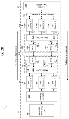
On-package die-to-die (D2D) interconnect for memory using universal chiplet interconnect express (UCIE) phy
PatentWO2024196389A1
Innovation
- The implementation of a Universal Chiplet Interconnect Express (UCIe) PHY for on-package die-to-die interconnects, which enables high-bandwidth, low-latency, and power-efficient connectivity between semiconductor dies, including System-on-a-Chip (SoC) and memory ICs, by mapping standard memory signals to UCIe signals for transport over the UCIe interconnect, thereby scaling memory solutions across various applications from handheld devices to high-performance computing.

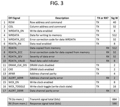
SYSTEMS AND METHODS FOR TRANSMITTING AND RECEIVING DOUBLE DATA RATE (DDR) PHYSICAL (PHY) INTERFACE (DFI) SIGNALS USING UNIVERSAL CHIPLET INTERCONNECT EXPRESS (UCIe)
PatentPendingUS20250258786A1
Innovation
- The use of a universal chiplet interconnect express (UCIe) interface for die-to-die communication, which converts DDR PHY interface signals to UCIe signals based on specific mappings, reducing power consumption and enhancing scalability by integrating fewer UCIe modules compared to traditional DDR PHY methods.

Standardization Efforts in Chiplet Interconnect Protocols
The standardization of chiplet interconnect protocols represents a critical evolution in semiconductor integration strategies, with UCIe (Universal Chiplet Interconnect Express) emerging as a leading standard. The consortium behind UCIe, formed in March 2022, includes industry giants such as Intel, AMD, Arm, TSMC, and Samsung, demonstrating broad industry commitment to establishing common protocols for die-to-die communication.
UCIe standardization efforts specifically address latency budgeting through a comprehensive framework that defines both physical and protocol layers. The standard establishes specific timing parameters for die-to-die communication, with latency targets categorized into standard, advanced, and ultra-low latency profiles to accommodate diverse application requirements from high-performance computing to real-time systems.
Competing standards have also emerged in the chiplet interconnect landscape. CCIX (Cache Coherent Interconnect for Accelerators), developed by the CCIX Consortium, focuses on cache coherency but typically exhibits higher latency compared to UCIe. CXL (Compute Express Link), maintained by the CXL Consortium, offers memory coherency features with competitive latency characteristics. OpenHBI (Open High Bandwidth Interface) represents another alternative with its focus on high-bandwidth applications.
The standardization process for UCIe involves rigorous validation through compliance testing and certification programs. These programs ensure interoperability between chiplets from different vendors, with specific test vectors designed to verify that die-to-die latency meets the specified budgets across various operating conditions and implementation scenarios.
Industry adoption of UCIe has accelerated due to its comprehensive approach to latency management. The standard's specification includes detailed timing budgets for different communication scenarios, providing clear guidelines for designers implementing chiplet-based systems. This standardization has enabled more predictable system performance and facilitated multi-vendor chiplet ecosystems.
Future standardization efforts are focusing on further refining latency specifications, with working groups dedicated to optimizing protocol efficiency and reducing overhead. Emerging proposals include dynamic latency adaptation mechanisms that would allow systems to adjust timing parameters based on workload requirements and power constraints, potentially enabling more efficient operation across diverse application scenarios.
Power-Performance Tradeoffs in Die-to-Die Communications
The power-performance tradeoff in die-to-die communications represents a critical design consideration in UCIe chiplet interconnect architectures. As data rates continue to increase, power consumption becomes a limiting factor that must be carefully balanced against performance requirements. The UCIe standard defines multiple physical interface options with varying power profiles, from ultra-low power modes operating at 16GT/s to high-performance modes reaching 32GT/s.
Signal integrity challenges directly impact this tradeoff, as maintaining clean signals at higher data rates typically requires more sophisticated equalization techniques that consume additional power. Advanced equalization methods such as Decision Feedback Equalization (DFE) and Continuous Time Linear Equalization (CTLE) can significantly improve signal quality but come with substantial power penalties, sometimes increasing power consumption by 20-30% compared to simpler schemes.
Voltage swing selection presents another critical tradeoff point. Higher voltage swings improve signal integrity and reduce bit error rates but increase power consumption quadratically. UCIe implementations must carefully select appropriate voltage levels based on channel characteristics and performance targets. Some implementations have demonstrated that reducing swing voltage by 15% can decrease power consumption by nearly 25%, albeit with potential reliability implications.
Clock distribution networks also significantly impact both power and performance metrics. Forwarded clock architectures offer lower latency but consume more power due to additional clock lanes, while embedded clock recovery systems reduce lane count but add latency overhead. Recent innovations in adaptive clocking schemes have shown promise in dynamically adjusting clock parameters based on workload demands, potentially reducing power by up to 18% during low-utilization periods.
Thermal considerations further complicate this relationship, as higher temperatures increase both static and dynamic power consumption while potentially degrading performance through increased resistance. Advanced packaging technologies like silicon interposers and embedded multi-die interconnect bridges (EMIB) offer improved thermal characteristics but introduce additional design complexities and manufacturing costs.
The industry trend shows increasing focus on energy-proportional die-to-die links that can dynamically scale power consumption based on bandwidth requirements. Techniques such as lane hibernation, frequency scaling, and adaptive voltage scaling are being integrated into UCIe implementations to optimize power efficiency across varying workloads, potentially improving energy efficiency by 30-40% compared to static designs.
Unlock deeper insights with Patsnap Eureka Quick Research — get a full tech report to explore trends and direct your research. Try now!
Generate Your Research Report Instantly with AI Agent
Supercharge your innovation with Patsnap Eureka AI Agent Platform!