UCIe Chiplet Interconnect Memory Chiplets Integration Approaches
SEP 1, 202510 MIN READ
Generate Your Research Report Instantly with AI Agent
Patsnap Eureka helps you evaluate technical feasibility & market potential.
UCIe Chiplet Interconnect Background and Objectives
The Universal Chiplet Interconnect Express (UCIe) emerged as a response to the growing challenges in traditional monolithic chip design. As Moore's Law faces physical limitations, the semiconductor industry has been shifting towards disaggregated chip architectures. This paradigm shift necessitated standardized interconnect protocols to enable seamless integration of heterogeneous chiplets from different vendors, leading to the development of UCIe.
UCIe represents a collaborative effort by industry leaders including Intel, AMD, ARM, TSMC, and Samsung to establish an open interconnect standard for chiplet-based designs. Formally introduced in March 2022, UCIe aims to create a unified ecosystem where chiplets from various manufacturers can interoperate efficiently, fostering innovation while reducing development costs and time-to-market.
The evolution of chiplet technology has progressed through several key phases. Initially, multi-chip modules (MCMs) provided basic integration capabilities. This was followed by 2.5D integration using silicon interposers, which improved interconnect density but at higher costs. The current generation focuses on advanced packaging technologies like EMIB (Embedded Multi-die Interconnect Bridge) and Foveros, which UCIe is designed to complement and standardize.
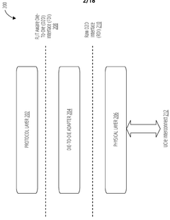
The primary objective of UCIe is to establish a comprehensive interconnect standard that addresses both physical and protocol layers for chiplet integration. At the physical layer, UCIe defines specifications for die-to-die interfaces, including bump pitches, power delivery, and signal integrity parameters. The protocol layer encompasses data transfer mechanisms, flow control, and error handling protocols essential for reliable communication between chiplets.
Memory integration represents a critical aspect of UCIe's objectives. As data-intensive applications drive demand for higher memory bandwidth and capacity, UCIe aims to facilitate efficient integration of memory chiplets with processing elements. This includes standardizing interfaces for HBM (High Bandwidth Memory), DDR, and emerging memory technologies, enabling flexible memory hierarchies tailored to specific application requirements.
Looking forward, UCIe targets scalability across multiple technology nodes and packaging approaches. The standard is designed to evolve with semiconductor technology, supporting future advancements in interconnect density, energy efficiency, and bandwidth. This forward-looking approach aims to ensure that UCIe remains relevant as chiplet technology continues to mature and diversify.
The ultimate goal of UCIe is to foster an open chiplet ecosystem that democratizes advanced semiconductor design, enabling smaller companies to compete effectively by focusing on their core competencies while leveraging standardized interfaces for system integration. This ecosystem approach promises to accelerate innovation while reducing the economic barriers to advanced semiconductor development.
UCIe represents a collaborative effort by industry leaders including Intel, AMD, ARM, TSMC, and Samsung to establish an open interconnect standard for chiplet-based designs. Formally introduced in March 2022, UCIe aims to create a unified ecosystem where chiplets from various manufacturers can interoperate efficiently, fostering innovation while reducing development costs and time-to-market.
The evolution of chiplet technology has progressed through several key phases. Initially, multi-chip modules (MCMs) provided basic integration capabilities. This was followed by 2.5D integration using silicon interposers, which improved interconnect density but at higher costs. The current generation focuses on advanced packaging technologies like EMIB (Embedded Multi-die Interconnect Bridge) and Foveros, which UCIe is designed to complement and standardize.
The primary objective of UCIe is to establish a comprehensive interconnect standard that addresses both physical and protocol layers for chiplet integration. At the physical layer, UCIe defines specifications for die-to-die interfaces, including bump pitches, power delivery, and signal integrity parameters. The protocol layer encompasses data transfer mechanisms, flow control, and error handling protocols essential for reliable communication between chiplets.
Memory integration represents a critical aspect of UCIe's objectives. As data-intensive applications drive demand for higher memory bandwidth and capacity, UCIe aims to facilitate efficient integration of memory chiplets with processing elements. This includes standardizing interfaces for HBM (High Bandwidth Memory), DDR, and emerging memory technologies, enabling flexible memory hierarchies tailored to specific application requirements.
Looking forward, UCIe targets scalability across multiple technology nodes and packaging approaches. The standard is designed to evolve with semiconductor technology, supporting future advancements in interconnect density, energy efficiency, and bandwidth. This forward-looking approach aims to ensure that UCIe remains relevant as chiplet technology continues to mature and diversify.
The ultimate goal of UCIe is to foster an open chiplet ecosystem that democratizes advanced semiconductor design, enabling smaller companies to compete effectively by focusing on their core competencies while leveraging standardized interfaces for system integration. This ecosystem approach promises to accelerate innovation while reducing the economic barriers to advanced semiconductor development.
Market Demand Analysis for Chiplet-based Solutions
The global chiplet market is experiencing unprecedented growth, driven by the increasing demand for high-performance computing solutions across various industries. As traditional monolithic chip designs approach their physical and economic limits, chiplet-based architectures have emerged as a compelling alternative. Market research indicates that the chiplet market is projected to grow at a CAGR of over 40% from 2023 to 2030, with the total addressable market expected to reach tens of billions of dollars by the end of the decade.
The primary market drivers for UCIe chiplet interconnect and memory chiplet integration include the escalating computational requirements of artificial intelligence and machine learning applications. These applications demand massive parallel processing capabilities and high-bandwidth memory access, which chiplet-based designs can efficiently deliver. Data centers and cloud service providers are particularly interested in chiplet solutions due to their potential for improved performance density and energy efficiency.
Consumer electronics manufacturers are also showing increased interest in chiplet technology as they seek to differentiate their products through enhanced performance while maintaining competitive pricing. The ability to mix and match chiplets from different process nodes and vendors offers unprecedented flexibility in product design and time-to-market advantages.
From a geographical perspective, North America currently leads the chiplet market, with major technology companies investing heavily in chiplet research and development. However, Asia-Pacific is expected to witness the fastest growth, driven by substantial investments in semiconductor manufacturing infrastructure and government initiatives to strengthen domestic chip production capabilities.
The automotive sector represents another significant market opportunity for chiplet-based solutions. Advanced driver-assistance systems (ADAS) and autonomous driving technologies require sophisticated computing platforms that can be efficiently implemented using chiplet architectures. The modular nature of chiplets allows automotive manufacturers to scale computing performance according to different vehicle models and price points.
Memory chiplet integration approaches are particularly valuable in data-intensive applications where memory bandwidth often becomes a bottleneck. High-bandwidth memory (HBM) chiplets connected via UCIe can significantly reduce latency and increase throughput compared to traditional memory architectures. This capability is driving adoption in high-performance computing, networking equipment, and enterprise storage systems.
Industry analysts predict that as the UCIe standard matures and the ecosystem expands, we will see accelerated adoption across multiple market segments. The standardization of chiplet interfaces is expected to reduce integration costs and risks, further expanding the market potential for chiplet-based solutions.
Current State and Challenges in Chiplet Interconnect Technologies
The global chiplet interconnect landscape is currently dominated by several key technologies, with UCIe (Universal Chiplet Interconnect Express) emerging as a promising standard for heterogeneous integration. UCIe 1.0, released in March 2022, represents a significant milestone in establishing an open industry standard for die-to-die interconnection. This standard supports both package-level and silicon-level interoperability, offering both standard and advanced modes with data rates ranging from 16 GT/s to 32 GT/s.
Competing with UCIe are several established proprietary solutions. AMD's Infinity Fabric has demonstrated success in their EPYC processors, while Intel's EMIB (Embedded Multi-die Interconnect Bridge) and Foveros technologies have enabled 2.5D and 3D integration respectively. TSMC's CoWoS (Chip-on-Wafer-on-Substrate) and InFO (Integrated Fan-Out) technologies have gained significant market traction, particularly in high-performance computing applications.
Memory chiplet integration presents unique challenges due to stringent bandwidth, latency, and power requirements. Current approaches include HBM (High Bandwidth Memory) integration via silicon interposers, which offers high bandwidth but at increased cost and complexity. Alternative solutions like Compute Express Link (CXL) are emerging for memory expansion and pooling, though with higher latency compared to direct integration methods.
The primary technical challenges in chiplet interconnect technologies center around several critical areas. Signal integrity issues become more pronounced at higher data rates, requiring sophisticated equalization techniques and careful impedance matching. Power delivery and thermal management across multiple chiplets demand innovative solutions, particularly as power densities increase with advanced process nodes.
Testing and known-good-die verification remain significant hurdles, as traditional testing methodologies are insufficient for complex multi-chiplet systems. The industry faces a lack of standardized testing protocols specifically designed for chiplet-based architectures, creating yield and reliability concerns.
Geographically, chiplet technology development shows distinct patterns. North America leads in interconnect architecture innovation through companies like Intel, AMD, and industry consortia. East Asia, particularly Taiwan and South Korea, dominates in advanced packaging implementation with TSMC, Samsung, and ASE as key players. Europe contributes significantly to standardization efforts and specialized applications through research institutions and companies like STMicroelectronics.
The economic constraints of chiplet implementation present another challenge. While chiplets promise cost advantages through improved yield and process optimization, the initial investment in design tools, testing infrastructure, and manufacturing capabilities remains substantial. This creates a barrier to entry for smaller companies and reinforces the dominance of established semiconductor giants in the chiplet ecosystem.
Current Memory Chiplet Integration Approaches
01 UCIe architecture for chiplet interconnection
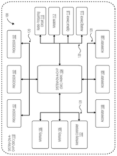
Universal Chiplet Interconnect Express (UCIe) provides a standardized architecture for connecting multiple chiplets within a package. This architecture enables high-bandwidth, low-latency communication between different chiplets, supporting both die-to-die and package-to-package connections. The UCIe standard defines physical layer specifications, protocols, and power management features that facilitate seamless integration of heterogeneous chiplets from different vendors, creating more modular and scalable semiconductor designs.- UCIe architecture for chiplet interconnection: Universal Chiplet Interconnect Express (UCIe) provides a standardized architecture for connecting multiple chiplets within a package. This architecture enables high-bandwidth, low-latency communication between different chiplets, supporting both die-to-die and package-to-package connections. The UCIe standard defines physical layer specifications, protocols, and electrical interfaces that facilitate seamless integration of heterogeneous chiplets from different vendors, creating more modular and flexible system designs.
- Memory chiplet integration techniques: Memory chiplets can be integrated with processing chiplets using various techniques to optimize system performance. These techniques include stacking memory chiplets vertically (3D integration), placing them side-by-side with processing chiplets (2.5D integration), or using interposers to connect them. Advanced packaging technologies such as silicon interposers, organic substrates, and through-silicon vias (TSVs) enable high-bandwidth connections between memory and processing chiplets while maintaining thermal efficiency and signal integrity.
- Power management and thermal solutions for chiplet designs: Effective power management and thermal solutions are critical for chiplet-based designs, especially when integrating memory chiplets that may have different power and thermal characteristics. Techniques include dynamic voltage and frequency scaling, power gating unused chiplets, implementing thermal sensors across the package, and using advanced cooling solutions. These approaches help maintain optimal performance while managing power consumption and preventing thermal issues that could affect reliability and performance of the integrated memory chiplets.
- Testing and validation methodologies for chiplet interconnects: Testing and validation methodologies specific to chiplet interconnects ensure reliable operation of integrated memory chiplets. These include pre-bond testing of individual chiplets, post-bond testing of the complete package, built-in self-test (BIST) circuits for interconnects, and boundary scan techniques. Advanced testing approaches can detect manufacturing defects, signal integrity issues, and timing violations in the high-speed interfaces between processing and memory chiplets, ensuring proper functionality of the final integrated system.
- Protocol optimization for memory chiplet communication: Protocol optimizations for memory chiplet communication focus on reducing latency and increasing bandwidth while maintaining compatibility with existing memory standards. These optimizations include streamlined command structures, efficient addressing schemes, reduced protocol overhead, and support for parallel operations. Advanced features such as speculative execution, prefetching mechanisms, and quality-of-service controls help maximize the performance benefits of integrated memory chiplets while ensuring data integrity and system reliability.
02 Memory chiplet integration techniques
Memory chiplet integration involves specialized techniques for connecting memory components with processing elements in multi-chiplet designs. These techniques include advanced packaging methods, interposer technologies, and specific interconnect protocols optimized for memory access patterns. By separating memory into dedicated chiplets, system designers can optimize memory capacity, bandwidth, and power efficiency independently from processing elements, while maintaining high-performance data transfer capabilities through specialized memory interfaces within the UCIe framework.Expand Specific Solutions03 Thermal management and power optimization for chiplet designs
Thermal management and power optimization are critical aspects of chiplet-based designs, especially when integrating memory chiplets with processing elements. These solutions include advanced cooling techniques, power delivery networks specifically designed for multi-chiplet packages, and dynamic power management systems that can adjust performance based on thermal conditions. The integration of thermal sensors, heat spreading materials, and power management controllers helps maintain optimal operating conditions across the entire chiplet assembly.Expand Specific Solutions04 Testing and validation methodologies for UCIe implementations
Testing and validation methodologies for UCIe implementations involve specialized techniques to verify the functionality, performance, and reliability of chiplet interconnects. These include die-to-die interface testing, signal integrity analysis, and protocol compliance verification. Advanced test structures embedded within chiplets allow for in-package testing of interconnects, while specialized test equipment and methodologies enable comprehensive validation of the entire chiplet assembly. These testing approaches ensure reliable operation of complex multi-chiplet systems under various operating conditions.Expand Specific Solutions05 Security features for chiplet-based systems
Security features for chiplet-based systems address the unique challenges of protecting data and intellectual property in disaggregated architectures. These include secure boot mechanisms for individual chiplets, authenticated communication channels between chiplets, encryption of die-to-die interfaces, and hardware-based security modules. The security architecture extends across the entire chiplet ecosystem, providing protection against physical tampering, side-channel attacks, and unauthorized access to sensitive data flowing between chiplets, while maintaining the performance benefits of the UCIe interconnect.Expand Specific Solutions
Key Industry Players in UCIe Ecosystem
The UCIe Chiplet Interconnect and Memory Chiplets Integration market is currently in its growth phase, characterized by rapid technological advancement and increasing industry adoption. The global chiplet market is projected to reach significant scale, driven by demands for higher performance computing and heterogeneous integration. Intel leads the UCIe consortium with substantial IP contributions, while TSMC, Samsung, and Micron are advancing memory chiplet technologies with different integration approaches. Qualcomm and AMD (formerly ATI) are focusing on mobile and high-performance computing applications respectively. Chinese players like Hygon and research institutions such as National University of Defense Technology are emerging as regional competitors, though still behind in technological maturity compared to established Western and Asian semiconductor giants.
Intel Corp.
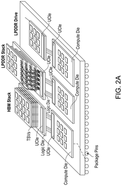
Technical Solution: Intel is a founding member and leading contributor to the UCIe (Universal Chiplet Interconnect Express) standard, which enables die-to-die interconnection across different process nodes and foundries. Their approach focuses on an open ecosystem for chiplet integration using advanced packaging technologies like EMIB (Embedded Multi-die Interconnect Bridge) and Foveros. Intel's UCIe implementation supports both package-level and die-to-die interconnects with data rates up to 32 GT/s and beyond. For memory chiplet integration, Intel has developed technologies like Ponte Vecchio that incorporate HBM (High Bandwidth Memory) chiplets alongside compute tiles using their advanced packaging solutions. Their Co-EMIB technology combines multiple packaging approaches to enable complex heterogeneous integration of memory and compute chiplets. Intel has also demonstrated silicon photonics integration with UCIe for future bandwidth scaling beyond electrical interconnects.
Strengths: Industry-leading packaging technologies (EMIB, Foveros) that provide flexibility in chiplet integration; strong IP portfolio in interconnect technologies; established manufacturing capabilities. Weaknesses: Higher implementation costs compared to monolithic designs; thermal management challenges in densely packed chiplet designs; potential yield issues with complex multi-chiplet packages.
QUALCOMM, Inc.
Technical Solution: Qualcomm has developed a comprehensive UCIe-compatible chiplet integration strategy focused on mobile and edge computing applications. Their approach leverages advanced 3D stacking technologies and their proprietary Network-on-Chip (NoC) architecture to enable efficient communication between heterogeneous chiplets. Qualcomm's memory integration approach emphasizes power efficiency, utilizing both HBM for high-performance applications and custom low-power memory chiplets for mobile devices. Their technology implements fine-grained power management across chiplet boundaries, allowing dynamic power allocation based on workload requirements. Qualcomm has demonstrated UCIe-based designs that achieve up to 4x better power efficiency compared to traditional SoC implementations while maintaining comparable performance. Their memory integration techniques include advanced TSV (Through-Silicon Via) implementations and microbump arrays optimized for mobile form factors, with interconnect pitches below 40μm to maximize density.
Strengths: Industry-leading power efficiency optimized for mobile applications; extensive experience with heterogeneous integration; strong IP in mobile SoC design that transfers to chiplet architecture. Weaknesses: Less experience with high-performance computing applications compared to competitors; potentially higher unit costs due to specialized packaging requirements; more limited manufacturing capacity compared to larger IDMs.
Core Patents and Technical Literature on UCIe
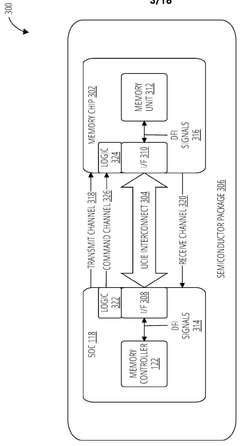
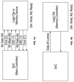
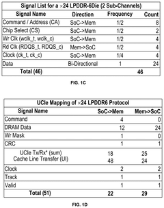
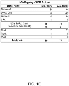
On-package die-to-die (D2D) interconnect for memory using universal chiplet interconnect express (UCIE) phy
PatentWO2024196389A1
Innovation
- The implementation of a Universal Chiplet Interconnect Express (UCIe) PHY for on-package die-to-die interconnects, which enables high-bandwidth, low-latency, and power-efficient connectivity between semiconductor dies, including System-on-a-Chip (SoC) and memory ICs, by mapping standard memory signals to UCIe signals for transport over the UCIe interconnect, thereby scaling memory solutions across various applications from handheld devices to high-performance computing.

On-package memory with universal chiplet interconnect express
PatentPendingUS20250123990A1
Innovation
- The implementation of Universal Chiplet Interconnect Express (UCIe) enhances memory interfacing by standardizing connections between processors and various memory types, optimizing communication, and integrating memory controllers on the same package to increase bandwidth and reduce latency.
Thermal Management Considerations for Chiplet Designs
Thermal management has emerged as a critical challenge in chiplet-based designs, particularly for UCIe (Universal Chiplet Interconnect Express) implementations and memory chiplet integration. As chiplet technology enables higher integration densities and performance levels, the resulting thermal density increases significantly, creating potential hotspots that can compromise system reliability and performance.
The thermal challenges in UCIe-based designs stem from several factors. First, the close proximity of multiple chiplets increases thermal density compared to traditional monolithic designs. Second, the heterogeneous nature of chiplet integration means different components generate heat at varying rates, creating uneven thermal profiles. Third, the interposer or substrate materials used for chiplet integration often have different thermal conductivity properties than silicon, complicating heat dissipation pathways.
Memory chiplets present unique thermal considerations due to their operational characteristics. DRAM-based memory chiplets are particularly sensitive to temperature variations, with performance and reliability degrading at elevated temperatures. HBM (High Bandwidth Memory) stacks, commonly used in high-performance computing applications with UCIe, create vertical thermal gradients that require specialized cooling solutions.
Current thermal management approaches for chiplet designs include advanced thermal interface materials (TIMs) that maximize heat transfer between chiplets and heat spreaders. These materials have evolved to include metal-based TIMs with thermal conductivity exceeding 20 W/m·K, significantly improving heat dissipation compared to traditional polymer-based solutions. Liquid cooling solutions are increasingly being deployed for high-performance chiplet designs, with direct liquid cooling to the back of silicon showing promising results for UCIe implementations.
Thermal modeling and simulation have become essential tools in chiplet design workflows. Computational fluid dynamics (CFD) simulations coupled with detailed power models enable accurate prediction of thermal hotspots and inform placement decisions for chiplets with different power profiles. Advanced thermal sensors embedded within chiplets provide real-time temperature monitoring, enabling dynamic thermal management through frequency and voltage scaling.
Future thermal management innovations for UCIe and memory chiplet designs are focusing on integrated microfluidic cooling channels within interposers, which could provide cooling capacity exceeding 500 W/cm². Additionally, phase-change cooling materials embedded between chiplets show promise for managing transient thermal loads. Three-dimensional heat spreading structures using diamond or graphene materials are being explored to address the anisotropic thermal conductivity challenges in stacked chiplet configurations.
The industry is moving toward holistic thermal management approaches that consider thermal constraints from the earliest stages of chiplet architecture planning through physical implementation, recognizing that thermal considerations are no longer secondary concerns but primary design constraints in the chiplet era.
Manufacturing and Testing Challenges for Multi-chiplet Systems
The manufacturing and testing of multi-chiplet systems present significant challenges that require innovative solutions and methodologies. The transition from monolithic designs to chiplet-based architectures introduces complexity across the entire production pipeline, from fabrication to final testing.
Manufacturing challenges begin with the precise alignment requirements for chiplet placement. UCIe (Universal Chiplet Interconnect Express) specifications demand micron-level accuracy to ensure proper bump connections between chiplets. This necessitates advanced pick-and-place equipment with exceptional precision capabilities. The manufacturing process must also account for thermal expansion coefficients of different materials, as mismatches can lead to mechanical stress and connection failures during operation.
Die-to-die bonding represents another critical manufacturing hurdle. Whether using micro-bump, hybrid bonding, or direct copper-to-copper connections, each approach requires specialized equipment and processes. Hybrid bonding, while offering superior electrical performance for UCIe implementations, demands extremely clean and planar surfaces with sub-nanometer roughness tolerances.
Yield management becomes increasingly complex in multi-chiplet systems. While chiplet architectures theoretically improve overall yield by allowing smaller die sizes, the integration process introduces new failure points. A single defective chiplet or interconnect can render an entire package unusable, necessitating sophisticated known-good-die testing methodologies before integration.
Testing challenges are equally significant. Traditional boundary scan techniques are insufficient for the high-speed, high-density interconnects used in UCIe implementations. Memory chiplet integration introduces additional testing complexities, requiring verification of both the memory components and their interconnections with processing elements. Built-in self-test (BIST) circuits must be incorporated into chiplet designs, consuming valuable silicon area but providing essential test capabilities.
Thermal testing presents unique challenges in heterogeneous integration scenarios. Different chiplets may have varying thermal characteristics and power densities, creating hotspots and thermal gradients that are difficult to predict and test. Advanced thermal simulation and testing methodologies are required to ensure reliable operation across diverse workloads and environmental conditions.
Signal integrity testing for high-speed UCIe links demands sophisticated equipment capable of characterizing connections operating at 16-32 GT/s. The close proximity of multiple chiplets can create electromagnetic interference issues that must be identified during testing phases. Additionally, testing memory chiplet integration requires verification of timing parameters across different process, voltage, and temperature conditions.
Unlock deeper insights with Patsnap Eureka Quick Research — get a full tech report to explore trends and direct your research. Try now!
Generate Your Research Report Instantly with AI Agent
Supercharge your innovation with Patsnap Eureka AI Agent Platform!