Design For Manufacturability In UCIe Chiplet Interconnect
SEP 1, 202510 MIN READ
Generate Your Research Report Instantly with AI Agent
Patsnap Eureka helps you evaluate technical feasibility & market potential.
UCIe Chiplet Interconnect Background and Objectives
Universal Chiplet Interconnect Express (UCIe) represents a significant paradigm shift in semiconductor design and manufacturing, emerging as a response to the slowing of Moore's Law and the increasing challenges in traditional monolithic chip scaling. The evolution of semiconductor technology has reached a critical juncture where chiplet-based designs offer a more viable path forward for continued performance improvements and cost optimization.
The UCIe standard, initially announced in March 2022, was developed by a consortium of industry leaders including Intel, AMD, Arm, TSMC, and Samsung, among others. This collaborative effort aims to establish an open, industry-standard die-to-die interconnect that enables the mixing and matching of chiplets from different vendors within a single package, fostering innovation and competition in the semiconductor ecosystem.
Historically, semiconductor advancement has been driven by process node shrinking, but as we approach physical limits, the industry has pivoted toward heterogeneous integration. This approach allows for combining different process technologies optimized for specific functions, rather than compromising on a single monolithic design. UCIe builds upon previous interconnect technologies such as Intel's AIB (Advanced Interface Bus) and EMIB (Embedded Multi-die Interconnect Bridge), but with a crucial focus on standardization and interoperability.
The primary objective of UCIe is to create a comprehensive ecosystem that supports chiplet-based designs with standardized physical interfaces, protocols, and testing methodologies. This standardization aims to reduce design complexity, lower development costs, and accelerate time-to-market for advanced semiconductor products. By enabling a "plug-and-play" approach to chiplet integration, UCIe seeks to democratize access to cutting-edge semiconductor technology.
From a technical perspective, UCIe defines both package-level interconnects (for chiplets within the same package) and board-level interconnects (for communication between packages). The standard encompasses physical layer specifications, die-to-die I/O protocols, and software abstraction layers, providing a complete framework for chiplet integration.
The technology trajectory for UCIe includes progressive improvements in bandwidth density, power efficiency, and latency reduction. The initial UCIe 1.0 specification supports data rates up to 32 GT/s, with future iterations expected to push beyond 64 GT/s while maintaining backward compatibility. This evolutionary path ensures that investments in UCIe-compliant designs remain protected as the standard advances.
A critical aspect of UCIe's objectives is addressing the manufacturability challenges inherent in chiplet-based designs. These include precise die placement, thermal management across heterogeneous components, testing methodologies for known-good-die, and yield optimization strategies for multi-die packages. Solving these manufacturing challenges is essential for the widespread adoption of chiplet technology across various market segments.
Market Demand Analysis for Chiplet-Based Solutions
The global semiconductor industry is witnessing a paradigm shift from traditional monolithic system-on-chip (SoC) designs to more modular chiplet-based architectures. This transition is primarily driven by the increasing complexity and cost of advanced semiconductor manufacturing processes. Market analysis indicates that the chiplet market is expected to grow at a compound annual growth rate of over 40% from 2023 to 2030, potentially reaching a market value of $50 billion by 2030.
The demand for UCIe (Universal Chiplet Interconnect Express) chiplet solutions is being fueled by several key factors. First, the slowdown of Moore's Law has made traditional scaling approaches less economically viable. Manufacturing costs for advanced nodes below 5nm have increased exponentially, making chiplet-based designs an attractive alternative for achieving performance improvements while managing costs effectively.
Data center operators and cloud service providers represent the largest market segment for chiplet-based solutions, accounting for approximately 45% of the current demand. These entities require high-performance computing capabilities with optimized power consumption, which chiplet architectures can deliver through specialized silicon dies working in concert. The hyperscalers like Google, Amazon, and Microsoft are increasingly developing custom silicon solutions using chiplet approaches to gain competitive advantages in AI and machine learning workloads.
Consumer electronics manufacturers constitute another significant market segment, particularly for mobile devices and edge computing applications. These manufacturers are seeking ways to incorporate more functionality into smaller form factors while maintaining reasonable power envelopes. UCIe chiplet solutions enable the integration of heterogeneous technologies (analog, RF, memory) alongside digital processing elements, creating more versatile and power-efficient devices.
The automotive sector represents an emerging market for chiplet-based solutions, driven by the increasing semiconductor content in modern vehicles. Advanced driver-assistance systems (ADAS) and autonomous driving capabilities require substantial computing power, which can benefit from the modular approach offered by chiplets. Industry forecasts suggest that semiconductor content in premium vehicles could exceed $1,000 per vehicle by 2025, with chiplet solutions capturing a growing share of this value.
Geographically, North America and East Asia dominate the market for chiplet solutions, with approximately 40% and 35% market share respectively. Europe follows with roughly 15% market share, primarily driven by automotive and industrial applications. The remaining 10% is distributed across other regions, with emerging economies showing increasing interest in developing domestic semiconductor capabilities through chiplet-based approaches.
The UCIe standard's open ecosystem approach is particularly appealing to system integrators and OEMs who seek to reduce vendor lock-in and create more flexible supply chains. Market surveys indicate that over 70% of semiconductor companies are exploring or actively developing chiplet-based products, highlighting the industry-wide recognition of this architectural approach as a key strategy for future growth.
UCIe Technology Status and Manufacturing Challenges
Universal Chiplet Interconnect Express (UCIe) represents a significant advancement in semiconductor integration technology, enabling heterogeneous chiplet-based designs that overcome the limitations of traditional monolithic approaches. Currently, UCIe technology is in its early adoption phase, with the 1.0 specification released in 2022 and the 1.1 specification expected to further refine the standard. The industry has witnessed growing momentum as major semiconductor companies including Intel, AMD, TSMC, Samsung, and Arm have joined the UCIe consortium, signaling broad industry support.
Despite this progress, UCIe faces several critical manufacturing challenges. The most significant hurdle is achieving and maintaining the ultra-fine pitch requirements for die-to-die interconnects, which demand sub-micron precision in alignment and bonding. Current manufacturing processes struggle to consistently deliver the 25-45 micron bump pitches required by UCIe specifications while maintaining acceptable yields. This challenge is compounded by the need for extremely precise die placement during assembly, where misalignments of even a few microns can result in connection failures.
Thermal management presents another substantial challenge, as the dense interconnect structures create heat dissipation bottlenecks. The thermal interface materials and cooling solutions must be carefully engineered to prevent performance degradation and reliability issues in chiplet-based designs. Additionally, the testing methodologies for UCIe implementations remain underdeveloped, with limited standardized approaches for validating die-to-die interconnect functionality both pre- and post-assembly.
The manufacturing ecosystem for UCIe is still evolving, with significant gaps in specialized equipment and processes. Advanced packaging facilities require substantial investments in new tools capable of handling the precision requirements of chiplet integration. The supply chain for UCIe manufacturing remains fragmented, with varying levels of readiness among substrate suppliers, assembly houses, and test providers.
Geographically, UCIe technology development is concentrated in several key regions. North America leads in architectural innovation through companies like Intel and AMD, while East Asia dominates in manufacturing capabilities, particularly through TSMC in Taiwan and Samsung in South Korea. Europe contributes significantly to testing and validation methodologies, though with less manufacturing presence.
Yield management represents perhaps the most pressing economic challenge, as defects in any single chiplet or interconnect can render entire multi-die packages unusable. This "known good die" problem is exacerbated by the limited reworkability of assembled chiplet packages, creating a manufacturing risk profile significantly different from traditional monolithic designs.
Current DFM Approaches for UCIe Implementation
01 Manufacturing techniques for UCIe chiplet interconnects
Various manufacturing techniques are employed to produce reliable UCIe chiplet interconnects. These include advanced packaging methods, precision alignment processes, and specialized bonding technologies that ensure proper connection between chiplets. The manufacturing processes focus on achieving high yield rates while maintaining the integrity of the interconnect structures, which is crucial for the overall performance of multi-chiplet systems.- Manufacturing techniques for UCIe chiplet interconnects: Various manufacturing techniques are employed to create reliable UCIe chiplet interconnects. These include advanced packaging methods, precise alignment processes, and specialized bonding technologies that ensure proper electrical connections between chiplets. The manufacturing processes focus on achieving high yield rates while maintaining the integrity of the interconnect structures, which is critical for the overall performance of multi-chiplet systems.
- Materials and structures for UCIe interconnects: The selection of materials and structural designs plays a crucial role in UCIe chiplet interconnect manufacturability. Advanced conductive materials, dielectric layers, and bump structures are utilized to create reliable interconnections. These materials must withstand thermal cycling, mechanical stress, and provide consistent electrical performance. Innovative structural designs help to minimize signal loss and improve the overall reliability of the chiplet-to-chiplet connections.
- Testing and quality control for UCIe interconnects: Comprehensive testing and quality control methodologies are essential for ensuring the manufacturability of UCIe chiplet interconnects. These include electrical testing, physical inspection, reliability assessment, and defect analysis techniques. Advanced imaging and measurement tools are employed to verify the integrity of interconnects at various stages of the manufacturing process. These quality control measures help to identify and address potential issues before final assembly.
- Integration challenges and solutions for UCIe implementation: Implementing UCIe chiplet interconnects presents various integration challenges that require innovative solutions. These include addressing thermal management issues, signal integrity concerns, and power delivery constraints. Solutions involve optimized floor planning, advanced thermal interface materials, and specialized design rules that accommodate the unique requirements of chiplet-based architectures. Successful integration strategies focus on balancing performance, power efficiency, and manufacturability.
- Standardization and compatibility in UCIe manufacturing: Standardization efforts are crucial for ensuring compatibility and manufacturability across different UCIe chiplet implementations. This includes adherence to established specifications for physical dimensions, electrical parameters, and communication protocols. Standardized manufacturing processes and design methodologies help to create an ecosystem where chiplets from different vendors can be integrated seamlessly. These standards also facilitate testing, validation, and quality assurance across the supply chain.
02 Materials and structures for UCIe interconnects
The selection of materials and structural designs plays a critical role in UCIe chiplet interconnect manufacturability. Advanced conductive materials, dielectric layers, and bump structures are utilized to create reliable connections between chiplets. These materials must withstand thermal cycling, mechanical stress, and provide consistent electrical performance. Innovative structural designs help optimize signal integrity while facilitating efficient manufacturing processes.Expand Specific Solutions03 Testing and quality control for UCIe interconnects
Comprehensive testing and quality control methodologies are essential for ensuring the reliability of UCIe chiplet interconnects. These include electrical testing, physical inspection, and stress testing to identify potential failure points. Advanced imaging techniques and automated test equipment are employed to verify proper alignment, connection integrity, and performance characteristics of the interconnects before final assembly into systems.Expand Specific Solutions04 Integration challenges and solutions for UCIe implementation
Implementing UCIe chiplet interconnects presents several integration challenges that require innovative solutions. These include thermal management issues, signal integrity concerns, and compatibility with existing manufacturing infrastructure. Solutions involve specialized design rules, thermal interface materials, and modified assembly processes that address these challenges while maintaining manufacturability at scale.Expand Specific Solutions05 Scalability and standardization of UCIe manufacturing
Achieving scalable manufacturing processes for UCIe chiplet interconnects requires standardization across the industry. This includes developing common specifications for interconnect dimensions, electrical characteristics, and testing methodologies. Standardization efforts focus on creating manufacturing processes that can be implemented across different fabrication facilities while maintaining consistent quality and performance, enabling broader adoption of chiplet-based architectures.Expand Specific Solutions
Key Industry Players in Chiplet Ecosystem
The UCIe chiplet interconnect market is in its early growth phase, characterized by rapid technological development and increasing industry adoption. The market size is expanding significantly as chiplet-based designs become essential for advanced computing solutions, with projections indicating substantial growth over the next five years. Regarding technical maturity, industry leaders Intel, TSMC, and AMD (through Xilinx) are at the forefront, having developed comprehensive DFM methodologies for chiplet integration. Qualcomm and Samsung are advancing quickly with their heterogeneous integration capabilities, while newer entrants like Jariet Technologies are focusing on specialized RF/microwave transceiver chiplets. SMIC and SK hynix are also making strategic investments to establish their positions in this emerging ecosystem, though they currently lag behind the established leaders in manufacturing readiness and integration capabilities.
Intel Corp.
Technical Solution: Intel has pioneered UCIe (Universal Chiplet Interconnect Express) as a founding member of the UCIe consortium. Their approach to Design for Manufacturability (DFM) in UCIe focuses on standardizing die-to-die interfaces while optimizing for high-volume manufacturing. Intel's Embedded Multi-die Interconnect Bridge (EMIB) technology serves as a foundation for their UCIe implementation, allowing for high-density connections between chiplets with reduced manufacturing complexity. They've developed specific DFM guidelines addressing thermal management, power delivery, and signal integrity across chiplet boundaries. Intel's Advanced Interface Bus (AIB) protocol has been adapted to work within the UCIe framework, providing compatibility with their existing manufacturing infrastructure while supporting the new standard. Their manufacturing approach includes specialized test structures for validating die-to-die connections and automated optical inspection techniques specifically calibrated for chiplet interfaces[1][3].
Strengths: Extensive manufacturing infrastructure and experience with heterogeneous integration; established ecosystem of partners familiar with their manufacturing processes. Weaknesses: Proprietary aspects of their implementation may create compatibility challenges with other vendors' chiplets; higher manufacturing costs compared to monolithic designs.
QUALCOMM, Inc.
Technical Solution: Qualcomm has developed a comprehensive DFM strategy for UCIe implementation focusing on mobile and edge computing applications. Their approach emphasizes power efficiency and thermal optimization critical for battery-powered devices. Qualcomm's UCIe implementation incorporates their expertise in package-on-package technology, adapting it for chiplet-based designs with specialized manufacturing considerations for ultra-thin packages. They've created a modular testing framework that allows individual chiplets to be validated before final assembly, reducing manufacturing yield issues. Qualcomm's DFM guidelines for UCIe include specific parameters for die alignment tolerances, microbump pitch optimization, and underfill material selection tailored for mobile device thermal cycles. Their manufacturing process incorporates AI-based defect detection specifically trained on chiplet interconnect patterns to identify potential reliability issues before final packaging[2][5].
Strengths: Expertise in power-efficient designs and mobile-specific manufacturing constraints; established supply chain relationships for high-volume production. Weaknesses: Less experience with high-performance computing applications that may require different DFM considerations; potential challenges with thermal management in densely packed chiplet designs.
Critical Patents and Technologies in UCIe Manufacturing
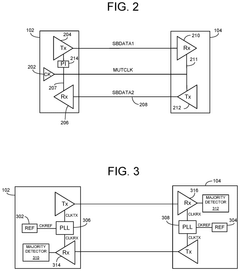
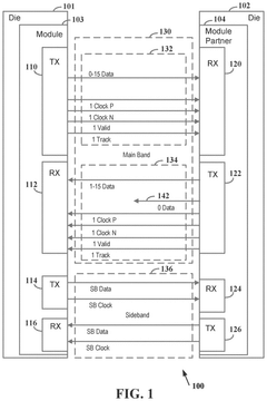
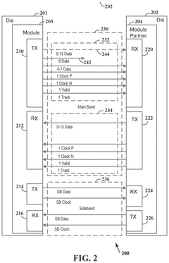
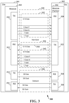
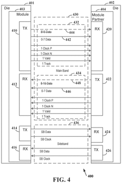
Interface conversion circuitry for universal chiplet interconnect express (UCIe)
PatentActiveUS12248419B1
Innovation
- The implementation of a converter circuit between the UCIe interface circuit and the bump interface, which includes local clock circuitry, oversampling circuitry, and majority detection circuitry, reduces the number of sideband links and corresponding bumps, thereby enhancing bandwidth density and reducing costs.
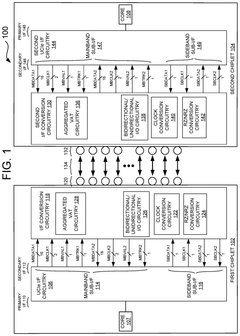
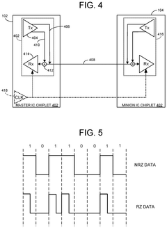
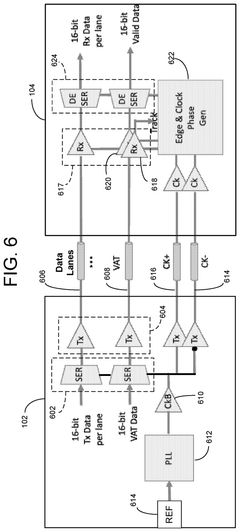
Variable link width in two directions for main band chip module connection
PatentPendingUS20240354279A1
Innovation
- Implementing a method to establish a die-to-die connection with a variable link width, allowing for independent configuration of transmit and receive data lanes through a sideband communication, enabling operation with different numbers of active data lanes in each direction to optimize power usage and data rates, and supporting fault tolerance by excluding faulty lines.
Supply Chain Considerations for UCIe Adoption
The adoption of UCIe (Universal Chiplet Interconnect Express) technology necessitates careful consideration of supply chain dynamics to ensure successful implementation and scalability. The fragmentation of traditional monolithic designs into chiplets introduces new complexities in sourcing, manufacturing, and integration processes that organizations must navigate strategically.
Supply chain resilience represents a critical factor in UCIe adoption. Companies implementing chiplet-based designs must develop robust multi-sourcing strategies for die components, packaging materials, and testing equipment. The geographical distribution of manufacturing capabilities for advanced packaging technologies remains concentrated in East Asia, creating potential vulnerabilities that require diversification efforts to mitigate geopolitical and natural disaster risks.
Inventory management practices require significant adaptation when transitioning to chiplet-based designs. The modular nature of chiplets enables more flexible inventory strategies, allowing manufacturers to maintain stocks of standardized chiplet components rather than complete SoCs. This approach can reduce obsolescence risks and improve responsiveness to market demands, though it necessitates sophisticated tracking systems to manage the increased component complexity.
Quality control presents unique challenges in the UCIe supply chain. The integration of chiplets from multiple vendors demands standardized testing protocols and clear accountability frameworks. Leading semiconductor manufacturers are establishing certification programs for UCIe-compliant components, while developing specialized testing equipment capable of validating high-bandwidth die-to-die interconnects at production scales.
Cost structures shift significantly with UCIe implementation. While individual chiplet production may benefit from higher yields and specialized manufacturing processes, the additional packaging and integration steps introduce new cost centers. Organizations must develop comprehensive total cost of ownership models that account for testing, yield impacts, and potential supply chain disruptions when evaluating UCIe adoption strategies.
Intellectual property management becomes increasingly complex in the chiplet ecosystem. Clear IP frameworks and licensing models are essential for fostering collaboration while protecting proprietary technologies. Industry consortia are working to establish standard interfaces and protocols that enable interoperability without compromising competitive advantages in core chiplet designs.
The transition timeline for supply chain partners represents a strategic consideration for UCIe adopters. Semiconductor manufacturers, packaging houses, and testing facilities require significant lead time to develop capabilities aligned with UCIe specifications. Early engagement with key suppliers and collaborative roadmap development can mitigate risks associated with capacity constraints and technical readiness.
Cost-Performance Tradeoffs in Chiplet Integration
The integration of chiplets through UCIe (Universal Chiplet Interconnect Express) presents significant cost-performance tradeoffs that must be carefully evaluated during the design and manufacturing process. While chiplet architecture offers promising advantages in terms of scalability and flexibility, manufacturers must balance these benefits against the economic implications of implementation.
Manufacturing costs for UCIe-based chiplet designs are influenced by several key factors. Die disaggregation introduces additional testing requirements at multiple stages, increasing overall quality assurance expenses. The bumping and packaging processes for chiplet integration demand high-precision equipment and specialized materials, particularly for achieving the fine-pitch interconnects specified by the UCIe standard. These manufacturing considerations directly impact the final product cost structure.
Performance optimization in chiplet designs often requires additional silicon area for interface circuitry, power delivery networks, and thermal management solutions. The UCIe standard's physical layer implementations vary in complexity and cost, with advanced implementations offering higher bandwidth but requiring more sophisticated manufacturing processes. This creates a spectrum of design choices where manufacturers must determine the appropriate balance between performance capabilities and production economics.
Yield considerations play a crucial role in the cost-performance equation. Smaller chiplets typically achieve higher manufacturing yields compared to monolithic designs, potentially reducing costs through improved silicon utilization. However, this advantage must be weighed against the increased complexity in system integration and the potential for yield losses during the assembly process. The economic viability of chiplet designs depends heavily on optimizing this yield-cost relationship.
Time-to-market factors also influence the cost-performance calculus. While chiplet designs may accelerate product development through IP reuse and parallel development workflows, they introduce new manufacturing challenges that can impact production schedules. Companies must evaluate whether the potential market advantages of faster deployment outweigh the initial investment in UCIe manufacturing infrastructure.
Supply chain considerations further complicate the cost-performance analysis. The disaggregated nature of chiplet designs creates opportunities for specialized manufacturing partnerships but also introduces dependencies on multiple suppliers. Organizations implementing UCIe-based designs must develop robust supply chain strategies that balance cost efficiency against resilience and quality control requirements.
The optimal cost-performance balance varies significantly based on application requirements, production volumes, and market positioning. High-performance computing applications may justify premium manufacturing processes to maximize interconnect bandwidth, while consumer electronics might prioritize cost optimization through simplified UCIe implementations. This application-specific optimization represents one of the most significant advantages of the chiplet approach when properly executed.
Unlock deeper insights with Patsnap Eureka Quick Research — get a full tech report to explore trends and direct your research. Try now!
Generate Your Research Report Instantly with AI Agent
Supercharge your innovation with Patsnap Eureka AI Agent Platform!