UCIe Chiplet Interconnect TSV And Hybrid Bonding Options Comparison
SEP 1, 20259 MIN READ
Generate Your Research Report Instantly with AI Agent
Patsnap Eureka helps you evaluate technical feasibility & market potential.
UCIe Chiplet Interconnect Evolution and Objectives
Universal Chiplet Interconnect Express (UCIe) represents a significant evolution in semiconductor integration technology, emerging from the growing need to overcome the limitations of traditional monolithic chip designs. The concept of chiplets—smaller, specialized silicon dies that can be combined into a single package—has gained momentum as Moore's Law faces increasing physical and economic constraints. UCIe was formally introduced in March 2022 as an open industry standard, backed by major industry players including Intel, AMD, Arm, TSMC, and Samsung.
The evolution of chiplet interconnect technology can be traced through several key phases. Initially, companies developed proprietary solutions such as Intel's EMIB (Embedded Multi-die Interconnect Bridge) and AMD's Infinity Fabric. These early implementations demonstrated the viability of disaggregated chip designs but lacked standardization. The formation of the UCIe consortium marked a pivotal shift toward establishing a unified approach to chiplet integration.
Prior to UCIe, other standards such as CCIX (Cache Coherent Interconnect for Accelerators) and CXL (Compute Express Link) addressed specific aspects of chip-to-chip communication but did not provide a comprehensive framework for chiplet integration. UCIe builds upon these foundations while specifically targeting the physical and protocol layers needed for efficient die-to-die communication within a package.
The primary objective of UCIe is to establish a complete standardized die-to-die interconnect that enables chiplets from different vendors to work together seamlessly. This "mix-and-match" capability aims to create an open chiplet ecosystem, allowing semiconductor companies to focus on their core competencies while leveraging specialized components from other manufacturers.
Technical objectives of UCIe include achieving high bandwidth density (up to 16 GT/s in UCIe 1.0), low latency connections, and energy efficiency measured in picojoules per bit. The standard encompasses both the physical layer specifications and protocol stack, supporting both standard and advanced packaging technologies.
From a business perspective, UCIe aims to reduce development costs and time-to-market by enabling reuse of validated chiplet designs. This modular approach allows companies to update specific components without redesigning entire systems, potentially extending product lifecycles and improving yield management.
Looking forward, UCIe's roadmap includes increasing data rates beyond the initial 16 GT/s specification, expanding protocol support, and enhancing compatibility with emerging packaging technologies such as hybrid bonding. The consortium continues to grow, reflecting the industry's recognition that standardized chiplet interconnects represent a critical path forward for semiconductor advancement in the post-Moore's Law era.
Market Demand Analysis for Chiplet Integration Solutions
The chiplet integration market is experiencing unprecedented growth driven by the semiconductor industry's shift from monolithic designs to disaggregated architectures. Current market analysis indicates that the global chiplet market is projected to reach $57 billion by 2035, with a compound annual growth rate exceeding 40% from 2023 to 2030. This explosive growth is primarily fueled by increasing demands for high-performance computing, artificial intelligence, and data center applications that require more efficient interconnect solutions.
The demand for advanced chiplet integration technologies, particularly UCIe (Universal Chiplet Interconnect Express), TSV (Through-Silicon Via), and hybrid bonding solutions, stems from several market imperatives. First, traditional Moore's Law scaling has become economically prohibitive, with advanced node development costs surpassing $500 million per node. Chiplet-based designs offer a cost-effective alternative by enabling the integration of heterogeneous dies manufactured at different process nodes.
Performance requirements across computing sectors are driving the need for higher bandwidth, lower latency interconnects between dies. Current market data shows that data centers and high-performance computing applications require interconnect bandwidths exceeding 2 TB/s with latencies under 2 nanoseconds - specifications that conventional packaging technologies cannot achieve. UCIe, TSV, and hybrid bonding technologies directly address these requirements.
Energy efficiency has become a critical market driver, particularly in data centers where power consumption represents a significant operational cost. Advanced chiplet interconnect technologies can reduce power consumption by up to 30% compared to traditional multi-chip modules, creating strong market pull from hyperscalers and cloud service providers seeking to optimize their total cost of ownership.
Supply chain resilience represents another significant market factor. The semiconductor industry's recent supply chain disruptions have highlighted the strategic advantage of disaggregated designs, which allow manufacturers to source different components from multiple suppliers, reducing dependency on single sources. Market surveys indicate that 78% of semiconductor companies are actively pursuing chiplet strategies partly for supply chain diversification.
The automotive and edge computing sectors are emerging as significant growth markets for chiplet technologies. These applications require high reliability, thermal performance, and integration density that advanced interconnect solutions can provide. Market forecasts suggest that automotive applications for chiplet-based designs will grow at 52% CAGR through 2028, driven by autonomous driving and advanced driver assistance systems requirements.
TSV and Hybrid Bonding Current Status and Challenges
Through Silicon Via (TSV) and hybrid bonding technologies represent critical advancements in chiplet interconnect solutions for the UCIe (Universal Chiplet Interconnect Express) ecosystem. Currently, TSV technology has reached relative maturity with widespread adoption in high-bandwidth memory (HBM) applications and 2.5D/3D integration. The industry has achieved TSV diameters ranging from 5-10μm with aspect ratios of 10:1 to 20:1, while leading manufacturers have demonstrated capabilities for even smaller dimensions approaching 2-3μm.
Despite this progress, TSV technology faces significant challenges including thermal management issues, stress-induced silicon deformation, and keep-out zones that reduce usable silicon area. The manufacturing process remains complex with high costs associated with etching, isolation, barrier deposition, and filling processes. Yield management continues to be problematic, particularly as TSV dimensions decrease and densities increase.
Hybrid bonding has emerged as a promising alternative, offering superior interconnect density with sub-1μm pitch capabilities compared to TSV's typical 40-50μm pitch. Leading-edge implementations have demonstrated pitches as small as 0.5μm, with roadmaps targeting further reductions to 0.3μm. This technology enables direct copper-to-copper connections without intermediate solder materials, resulting in lower resistance, improved electrical performance, and reduced power consumption.
Geographically, advanced TSV and hybrid bonding capabilities are concentrated among major semiconductor manufacturers in East Asia (particularly Taiwan, South Korea, and Japan), North America, and select European countries. TSMC, Samsung, Intel, and SK Hynix lead commercial deployment, while research institutions like IMEC, CEA-Leti, and Fraunhofer continue to push technological boundaries.
The current technical limitations for hybrid bonding include stringent surface cleanliness requirements, with contamination tolerances measured in angstroms. Wafer bow and topography must be controlled within nanometer-scale precision, presenting significant manufacturing challenges. Additionally, the technology demands extremely precise alignment capabilities (±0.2μm or better) and specialized bonding equipment operating in ultra-clean environments.
Both technologies face integration challenges with the UCIe standard, which aims to establish a universal die-to-die interconnect standard. While TSV offers proven reliability and established manufacturing processes, hybrid bonding provides superior electrical performance and density that better aligns with future UCIe roadmap requirements for ultra-high bandwidth connections between chiplets.
The industry is actively working to address yield, cost, and reliability concerns through improved process control, new materials development, and advanced inspection techniques. Recent innovations include temporary bonding solutions, enhanced metrology for sub-micron alignment, and development of low-temperature bonding processes to reduce thermal stress.
Comparative Analysis of TSV vs Hybrid Bonding Solutions
01 UCIe Chiplet Interconnect Architecture
Universal Chiplet Interconnect Express (UCIe) provides a standardized architecture for connecting multiple chiplets within a package. This technology enables high-bandwidth, low-latency communication between different chiplets, allowing for modular chip design. UCIe supports various physical layer implementations and protocol stacks, facilitating interoperability between chiplets from different manufacturers while maintaining high performance and power efficiency.- UCIe chiplet interconnect architecture and standards: Universal Chiplet Interconnect Express (UCIe) is a standardized architecture for chiplet-based designs that enables high-performance, energy-efficient communication between different chiplets in a package. The UCIe standard defines protocols, physical interfaces, and electrical specifications to ensure interoperability between chiplets from different vendors. This architecture supports high bandwidth, low latency connections while maintaining signal integrity across the interconnect, facilitating the development of modular semiconductor designs with improved performance and integration density.
- Through-Silicon Via (TSV) technology for 3D integration: Through-Silicon Via (TSV) technology enables vertical electrical connections that pass completely through a silicon wafer or die, allowing for three-dimensional integration of semiconductor devices. TSVs provide shorter interconnect paths between stacked dies, resulting in reduced signal delay, lower power consumption, and higher bandwidth compared to traditional wire bonding. This technology significantly increases integration density by enabling the stacking of multiple dies in a single package, making it particularly valuable for applications requiring high performance in a compact form factor.
- Hybrid bonding interconnect techniques: Hybrid bonding interconnect technology combines dielectric-to-dielectric and metal-to-metal bonding to create high-density, high-performance connections between semiconductor components. This approach enables direct copper-to-copper connections at room temperature with subsequent annealing, eliminating the need for solder bumps or other intermediate materials. Hybrid bonding achieves finer pitch interconnects than traditional flip-chip methods, resulting in higher connection density, improved electrical performance, and enhanced thermal characteristics for advanced packaging solutions.
- Integration density optimization techniques: Various techniques are employed to optimize integration density in advanced semiconductor packaging, including fine-pitch interconnects, redistribution layers, and innovative die placement strategies. These approaches minimize the space between chiplets, maximize the utilization of package area, and enable more efficient routing of signals. Advanced lithography and etching processes allow for creating smaller interconnect features, while novel package architectures support higher component density without compromising thermal performance or signal integrity.
- Performance enhancement for chiplet-based systems: Performance enhancement techniques for chiplet-based systems focus on optimizing data transfer rates, reducing latency, and improving power efficiency across interconnects. These include advanced signaling methods, equalization techniques, and clock distribution strategies that maintain signal integrity at high frequencies. Additionally, specialized interface circuits, buffer designs, and power delivery networks are implemented to support high-bandwidth communication between chiplets while managing thermal constraints and ensuring reliable operation under various conditions.
02 Through-Silicon Via (TSV) Technology
TSV technology enables vertical electrical connections passing completely through silicon wafers or dies, creating 3D integrated circuits. This approach significantly reduces interconnect length compared to traditional 2D designs, resulting in improved signal integrity, reduced power consumption, and increased bandwidth. TSV implementation allows for higher integration density by stacking multiple dies vertically, making it particularly valuable for memory-logic integration and high-performance computing applications.Expand Specific Solutions03 Hybrid Bonding Interconnect Performance
Hybrid bonding technology enables direct copper-to-copper connections between wafers or dies with minimal interface layers, resulting in superior electrical performance compared to traditional microbump approaches. This technology achieves extremely fine interconnect pitches, significantly improving connection density while reducing parasitic capacitance and resistance. The direct metal-to-metal bonding process creates robust mechanical and electrical connections that enhance signal integrity, thermal performance, and overall system reliability.Expand Specific Solutions04 Integration Density Optimization Techniques
Advanced packaging technologies enable significant improvements in integration density through various techniques including fine-pitch interconnects, multi-tier stacking, and interposer-based designs. These approaches allow for heterogeneous integration of different chiplets manufactured using optimal process nodes for each function. By combining high-density interconnects with innovative thermal management solutions, these techniques achieve unprecedented component density while maintaining signal integrity and power efficiency.Expand Specific Solutions05 Performance Enhancement and Power Management
Advanced chiplet interconnect technologies incorporate sophisticated power management features and performance optimization techniques. These include dynamic voltage and frequency scaling, power gating for unused components, and intelligent thermal management. The reduced interconnect length in advanced packaging solutions minimizes signal propagation delays and power consumption, while specialized I/O circuits optimize signal integrity across die boundaries. These technologies collectively enable higher bandwidth, lower latency, and improved energy efficiency compared to traditional monolithic designs.Expand Specific Solutions
Key Industry Players in Chiplet Interconnect Ecosystem
The UCIe Chiplet Interconnect market is currently in its early growth phase, characterized by rapid technological development and increasing industry adoption. The market is projected to expand significantly as chiplet architectures become essential for advanced computing systems, with an estimated value reaching several billion dollars by 2025. In terms of technical maturity, the industry is transitioning from proof-of-concept to commercial implementation, with key players driving innovation in different bonding technologies. Leading semiconductor companies like QUALCOMM, IBM, and Xilinx are advancing TSV technologies, while research institutions such as IMEC and Shanghai Institute of Microsystem & Information Technology are pioneering hybrid bonding solutions. GlobalFoundries and SMIC are developing manufacturing capabilities to support both approaches, creating a competitive landscape where technical differentiation and IP portfolios (notably from Rambus and Adeia) will determine market leadership.
QUALCOMM, Inc.
Technical Solution: Qualcomm has pioneered UCIe chiplet interconnect solutions focusing on mobile and edge computing applications. Their approach balances performance with power efficiency, utilizing a combination of micro-bump technology for standard connections and advanced hybrid bonding for high-performance interfaces. Qualcomm's UCIe implementation achieves approximately 1.5 TB/s/mm² bandwidth density with power consumption around 0.7 pJ/bit. Their TSV technology employs high aspect ratio vias (10:1) with diameters of approximately 5μm, enabling dense vertical connections while minimizing silicon area impact. Qualcomm has developed a proprietary "adaptive power management" system for their chiplet interconnects that dynamically adjusts signaling voltage and frequency based on bandwidth demands, further optimizing power efficiency. Their solution includes built-in test and repair mechanisms to improve manufacturing yield and reliability, particularly important for hybrid bonding processes where defect management is critical.
Strengths: Excellent power efficiency optimized for mobile applications; mature manufacturing ecosystem with established supply chain partners. Weaknesses: Somewhat lower bandwidth density compared to pure hybrid bonding solutions; thermal management challenges in compact mobile form factors.
Xilinx, Inc.
Technical Solution: Xilinx (now part of AMD) has developed specialized UCIe chiplet interconnect solutions optimized for FPGA and heterogeneous computing applications. Their approach leverages a hybrid architecture combining both TSV and hybrid bonding technologies to maximize flexibility and performance. Xilinx's "Stacked Silicon Interconnect" (SSI) technology has evolved to incorporate UCIe standards, achieving bandwidth densities of approximately 1.8 TB/s/mm² with latencies under 2.5ns. Their implementation uses a hierarchical approach with high-density hybrid bonding for critical high-bandwidth interfaces and more cost-effective micro-bump connections for less demanding pathways. Xilinx has developed specialized silicon interposers with embedded active components to enhance signal integrity and reduce power consumption in their chiplet designs. Their UCIe solution includes programmable PHY layers that can adapt to different protocols and electrical requirements, making it particularly suitable for heterogeneous integration scenarios where chiplets from different vendors and process nodes need to communicate efficiently.
Strengths: Highly flexible architecture suitable for heterogeneous integration; excellent signal integrity with advanced interposer technology. Weaknesses: More complex implementation requiring sophisticated design tools; higher initial engineering costs compared to monolithic solutions.
Critical Patents and Technical Innovations in Chiplet Interconnect
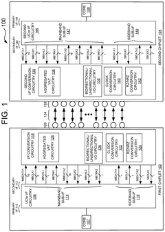
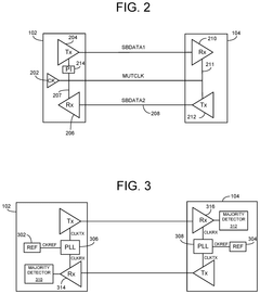
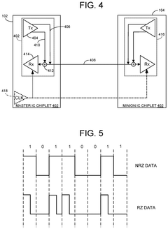
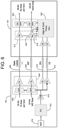
Interface conversion circuitry for universal chiplet interconnect express (UCIe)
PatentActiveUS12248419B1
Innovation
- The implementation of a converter circuit between the UCIe interface circuit and the bump interface, which includes local clock circuitry, oversampling circuitry, and majority detection circuitry, reduces the number of sideband links and corresponding bumps, thereby enhancing bandwidth density and reducing costs.
Interconnect with enhanced reliability and lifetime through reliability monitor and self repair
PatentWO2018004599A1
Innovation
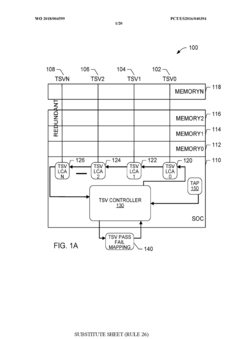
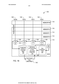
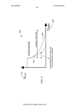
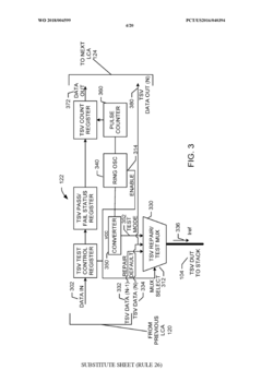
- An on-die reliability monitoring system that includes a current-based ring oscillator and counter to measure resistance changes, enabling in-field health monitoring and self-repair capabilities, allowing for predictive maintenance and replacement or modulation of TSVs before failures occur, thereby ensuring continuous circuit performance over time.
Manufacturing Yield and Cost Implications
Manufacturing yield and cost considerations are critical factors in determining the commercial viability of chiplet interconnect technologies. When comparing Through-Silicon Via (TSV) and hybrid bonding options for UCIe (Universal Chiplet Interconnect Express) implementations, yield implications significantly impact the overall economics of chiplet-based designs.
TSV technology, while more mature in production environments, presents notable yield challenges due to its complex manufacturing process. The creation of high aspect ratio vias through silicon substrates introduces potential defect sources including void formation, misalignment, and incomplete filling. Industry data suggests TSV implementations typically experience yield penalties of 5-10% compared to conventional packaging approaches, with this figure increasing for higher density TSV configurations.
Hybrid bonding, particularly direct copper-to-copper bonding, offers theoretical yield advantages through elimination of microbumps and underfill processes. However, the technology demands extremely stringent surface preparation requirements, with contamination tolerances measured in angstroms rather than microns. Current manufacturing data indicates hybrid bonding yield rates remain variable, ranging from 85-95% depending on process maturity and implementation specifics.
Cost structures differ significantly between these technologies. TSV manufacturing requires specialized etching, isolation, and filling equipment, with per-wafer processing costs estimated at 15-25% higher than standard wafer processing. The established infrastructure for TSV production provides some economies of scale, though capital expenditure requirements remain substantial.
Hybrid bonding presents a different cost profile, with lower material costs offset by higher precision equipment requirements. The ultra-clean room environments and specialized bonding tools represent significant capital investments, estimated at 1.5-2x those of comparable TSV production lines. However, the simplified assembly process potentially reduces per-unit costs at scale once yield targets are achieved.
Learning curve effects are particularly pronounced with hybrid bonding, where manufacturing experience correlates strongly with yield improvements. Industry leaders implementing hybrid bonding have reported yield improvements of 0.5-1% per quarter as processes mature, suggesting long-term cost advantages despite higher initial investments.
For high-volume applications, the cost crossover point between TSV and hybrid bonding appears to occur at approximately 100-150 million units, beyond which hybrid bonding's simplified assembly process and potential for higher interconnect densities begin to offset its higher initial costs. This economic inflection point continues to shift as both technologies evolve, with hybrid bonding's cost position improving as manufacturing processes mature and equipment costs amortize across larger production volumes.
Thermal Management Considerations for Chiplet Designs
Thermal management has emerged as a critical consideration in chiplet-based designs, particularly when implementing UCIe (Universal Chiplet Interconnect Express) with TSV (Through-Silicon Via) or hybrid bonding technologies. As chiplet architectures pack more computing power into smaller spaces, heat dissipation becomes increasingly challenging and directly impacts system performance, reliability, and lifespan.
The thermal characteristics of TSV and hybrid bonding technologies differ significantly. TSV implementations typically create more thermal resistance at interconnect points due to the physical structure of the vias and microbumps. This resistance can lead to localized hotspots that require targeted cooling solutions. In contrast, hybrid bonding offers superior thermal conductivity with its direct copper-to-copper connections, enabling more efficient heat transfer between chiplets.
Recent thermal simulation studies indicate that hybrid bonding can reduce junction temperatures by 5-10°C compared to equivalent TSV implementations under similar workloads. This temperature differential becomes particularly significant in high-performance computing applications where thermal throttling can substantially impact system capabilities.
Power density variations across chiplets present another thermal management challenge. In heterogeneous integration scenarios, combining high-power processing chiplets with memory or I/O chiplets creates uneven heat distribution. This necessitates sophisticated thermal management strategies including asymmetric cooling solutions and thermal-aware floorplanning to prevent thermal coupling between adjacent chiplets.
The choice of substrate and interposer materials significantly influences thermal performance. Silicon interposers offer better thermal conductivity than organic substrates, while advanced ceramic materials provide intermediate thermal performance with cost advantages. For UCIe implementations, silicon interposers typically provide better thermal performance but at higher manufacturing costs.
Active cooling technologies must be adapted specifically for chiplet architectures. Traditional heatsink and fan combinations may be insufficient for addressing the concentrated heat fluxes in chiplet designs. More advanced solutions including microfluidic cooling channels, integrated vapor chambers, and phase-change materials are being explored to manage the thermal challenges of densely packed chiplet systems.
Thermal management must also be considered during the early design phase through thermal-aware placement algorithms. These algorithms optimize chiplet positioning to minimize thermal coupling and hotspots while maintaining the electrical performance benefits of UCIe interconnects. Simulation tools that accurately model the thermal characteristics of both TSV and hybrid bonding technologies are essential for predicting thermal behavior before physical implementation.
Unlock deeper insights with Patsnap Eureka Quick Research — get a full tech report to explore trends and direct your research. Try now!
Generate Your Research Report Instantly with AI Agent
Supercharge your innovation with Patsnap Eureka AI Agent Platform!