Investor And CTO Briefing On UCIe Chiplet Interconnect
SEP 1, 20259 MIN READ
Generate Your Research Report Instantly with AI Agent
Patsnap Eureka helps you evaluate technical feasibility & market potential.
UCIe Chiplet Interconnect Background and Objectives
Universal Chiplet Interconnect Express (UCIe) represents a pivotal advancement in semiconductor integration technology, emerging as a response to the slowing of Moore's Law and the increasing challenges in traditional monolithic chip scaling. The evolution of semiconductor technology has historically followed a trajectory of increasing transistor density and performance improvements through process node advancements. However, as physical limitations have become more pronounced at sub-10nm nodes, the industry has been compelled to explore alternative approaches to continue delivering performance gains.
The concept of chiplets—smaller, specialized silicon dies that can be integrated into a single package—has gained significant traction as a viable path forward. This approach allows for the combination of different process technologies optimized for specific functions, enabling continued scaling of system performance and capabilities beyond what monolithic designs can achieve. The chiplet paradigm represents a fundamental shift from traditional System-on-Chip (SoC) designs to more modular and flexible System-in-Package (SiP) architectures.
UCIe was formally introduced in March 2022 as an open industry standard for die-to-die interconnection, backed by a consortium of major semiconductor companies including Intel, AMD, Arm, TSMC, Samsung, and others. This collaborative effort aims to establish a unified interconnect standard that enables chiplets from different vendors to work seamlessly together, fostering an open chiplet ecosystem and marketplace.
The primary technical objective of UCIe is to provide a standardized, high-bandwidth, energy-efficient interface for die-to-die communication within a package. The standard encompasses both the physical layer specifications and the protocol stack necessary for reliable data transfer between chiplets. UCIe supports both standard and advanced packaging technologies, including silicon interposers and organic substrates, making it adaptable to various integration approaches.
From a market perspective, UCIe aims to break down proprietary barriers in the semiconductor industry by enabling interoperability between chiplets from different vendors. This standardization is expected to accelerate innovation, reduce development costs, and shorten time-to-market for complex semiconductor products across various application domains including high-performance computing, artificial intelligence, data centers, and edge computing.
The long-term vision for UCIe extends beyond mere technical specifications to fundamentally transform the semiconductor value chain. By enabling a more modular approach to system design, UCIe has the potential to democratize silicon innovation, allowing smaller players to contribute specialized chiplets to the ecosystem without needing to develop complete SoC solutions. This could lead to more diverse and optimized semiconductor products while addressing the escalating costs and complexity of advanced node development.
Market Demand Analysis for Chiplet-Based Architectures
The chiplet-based architecture market is experiencing unprecedented growth, driven by the increasing demand for high-performance computing solutions across various industries. As traditional monolithic chip designs approach their physical and economic limits, chiplet technology has emerged as a compelling alternative that enables continued scaling of semiconductor capabilities while managing costs and manufacturing complexity.
Market research indicates that the global chiplet market is projected to grow at a CAGR of 40% from 2023 to 2030, reaching significant market valuation by the end of the forecast period. This explosive growth is primarily fueled by data centers and cloud service providers seeking more efficient and powerful computing solutions to handle AI workloads, big data analytics, and complex computational tasks.
The demand for chiplet-based architectures is particularly strong in the hyperscale data center segment, where companies are increasingly adopting disaggregated chip designs to optimize performance, power efficiency, and total cost of ownership. These organizations are willing to invest in advanced interconnect technologies like UCIe to achieve higher bandwidth, lower latency, and improved system integration.
Enterprise computing represents another substantial market segment, with businesses seeking more powerful servers and workstations to support their growing computational needs. The ability to mix and match chiplets from different process nodes and even different vendors presents an attractive value proposition for enterprise customers looking to customize their computing infrastructure.
Consumer electronics manufacturers are also showing interest in chiplet technology, particularly for high-end devices that require substantial computing power in compact form factors. The modular nature of chiplets allows for more flexible product designs and potentially faster time-to-market for new features.
From a regional perspective, North America currently leads the chiplet market due to the presence of major technology companies and semiconductor manufacturers. However, Asia-Pacific is expected to witness the fastest growth, driven by the expanding semiconductor ecosystem in countries like Taiwan, South Korea, and China.
The market demand is further accelerated by the increasing adoption of AI and machine learning technologies across industries. These applications require specialized computing architectures that can efficiently process massive datasets, making chiplet-based designs with heterogeneous integration particularly valuable.
Industry analysts note that the standardization efforts around UCIe are critical to unlocking the full market potential of chiplet technology. As the ecosystem matures and more companies adopt the standard, we can expect to see accelerated innovation and broader market adoption across various computing segments.
UCIe Technology Landscape and Implementation Challenges
The UCIe (Universal Chiplet Interconnect Express) technology landscape is rapidly evolving as the semiconductor industry shifts toward chiplet-based architectures. This transition is driven by the slowing of Moore's Law and the increasing costs of advanced process nodes, making monolithic chip designs less economically viable. UCIe represents a critical standardization effort to enable heterogeneous integration of chiplets from different vendors and process technologies.
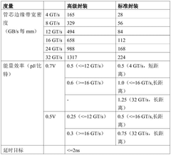
Currently, the UCIe ecosystem encompasses major semiconductor manufacturers including Intel, AMD, TSMC, Samsung, and Arm, who have joined the UCIe Consortium to establish an open standard for die-to-die interconnects. The standard focuses on both physical and protocol layers, supporting both package substrate and silicon interposer implementations with data rates up to 32 GT/s in its first iteration.
The implementation of UCIe faces several significant technical challenges. First, the physical integration of chiplets requires precise alignment and bonding techniques to ensure reliable connections between dies. This demands advanced packaging technologies such as EMIB (Embedded Multi-die Interconnect Bridge) or CoWoS (Chip-on-Wafer-on-Substrate) that can support the high-density interconnects required by UCIe.
Signal integrity presents another major challenge, particularly as data rates increase. Managing crosstalk, impedance matching, and power delivery across die boundaries requires sophisticated design techniques and potentially new materials. The thermal management of closely packed chiplets also becomes more complex, necessitating innovative cooling solutions.
Testing and validation of multi-chiplet systems introduce additional complexities. Traditional testing methodologies designed for monolithic chips must be adapted for chiplet architectures, requiring new approaches to known-good-die testing and system-level validation. This is particularly challenging when integrating chiplets from different vendors.
From a software perspective, memory coherence and efficient communication protocols between chiplets remain challenging. The UCIe standard addresses this through defined protocol layers, but implementing these efficiently in real-world designs requires careful optimization to minimize latency and maximize bandwidth.
The economic landscape also presents implementation hurdles. While UCIe aims to create an open ecosystem, questions remain about intellectual property rights, licensing models, and the establishment of a truly interoperable marketplace for chiplets. Companies must navigate these business considerations alongside technical implementation challenges.
Geographic distribution of UCIe technology development shows concentration in North America, East Asia, and Europe, with major research initiatives at both corporate and academic institutions. This global effort reflects the strategic importance of chiplet technology in the future semiconductor roadmap.
Current UCIe Technical Specifications and Implementation
01 UCIe architecture and standards for chiplet interconnection
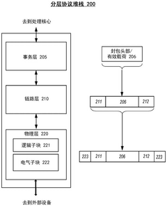
Universal Chiplet Interconnect Express (UCIe) provides a standardized architecture for connecting multiple chiplets within a package. This standard defines protocols, physical layer specifications, and electrical interfaces that enable high-speed, low-latency communication between different chiplets. The architecture supports both die-to-die and package-to-package interconnections, allowing for modular chip design and improved system performance.- UCIe architecture and standards for chiplet interconnection: Universal Chiplet Interconnect Express (UCIe) provides a standardized architecture for connecting multiple chiplets within a package. This standard defines protocols, physical layer specifications, and electrical interfaces to ensure interoperability between chiplets from different manufacturers. The architecture supports both die-to-die and package-to-package connections, enabling modular chip design with high-bandwidth, low-latency communication between components.
- Physical implementation of UCIe chiplet connections: The physical implementation of UCIe chiplet interconnects involves specific design considerations for bump patterns, trace routing, and signal integrity. These implementations include microbump arrays, through-silicon vias (TSVs), and redistribution layers (RDLs) that facilitate high-speed data transfer between chiplets. Advanced packaging technologies such as silicon interposers and bridge chips are used to optimize the physical connections while maintaining signal integrity across the chiplet interfaces.
- Power management and thermal solutions for UCIe implementations: Power management and thermal solutions are critical aspects of UCIe chiplet interconnect designs. These solutions include power delivery networks optimized for multi-chiplet packages, dynamic power management techniques that adjust power consumption based on workload demands, and thermal management strategies that address hotspots created by high-density interconnects. Advanced cooling solutions and power distribution architectures ensure reliable operation while maximizing performance efficiency in chiplet-based systems.
- Testing and validation methodologies for UCIe chiplet interconnects: Testing and validation methodologies for UCIe chiplet interconnects involve specialized techniques to ensure proper functionality and performance. These include built-in self-test (BIST) circuits, boundary scan testing, and high-speed signal integrity validation. Test structures are integrated into the chiplet designs to verify electrical characteristics, timing parameters, and protocol compliance. Advanced probe technologies and test fixtures are developed to access the dense interconnect structures during manufacturing and validation processes.
- Integration of UCIe with heterogeneous computing architectures: UCIe chiplet interconnects enable heterogeneous computing architectures by facilitating the integration of diverse processing elements such as CPUs, GPUs, FPGAs, and specialized accelerators. This integration supports disaggregated chip design where components can be manufactured using different process technologies optimized for their specific functions. The UCIe standard provides the communication framework that allows these diverse elements to work together efficiently, enabling system designers to create customized solutions for specific application domains while maintaining interoperability.
02 Physical implementation of UCIe chiplet interconnects
The physical implementation of UCIe chiplet interconnects involves specific design considerations for bump patterns, trace routing, and signal integrity. These implementations include advanced packaging technologies such as silicon interposers, organic substrates, and through-silicon vias (TSVs) to facilitate high-bandwidth connections between chiplets. The physical layer designs focus on minimizing signal degradation, reducing power consumption, and ensuring reliable data transmission across chiplet boundaries.Expand Specific Solutions03 Power management and thermal solutions for UCIe implementations
Power management and thermal solutions are critical aspects of UCIe chiplet interconnect implementations. These solutions include dynamic power scaling, thermal monitoring systems, and advanced cooling techniques to maintain optimal operating conditions for multi-chiplet packages. The designs incorporate power delivery networks specifically optimized for chiplet architectures, ensuring efficient power distribution while managing heat dissipation across the integrated components.Expand Specific Solutions04 Testing and validation methodologies for UCIe chiplet interconnects
Testing and validation methodologies for UCIe chiplet interconnects involve specialized techniques for verifying signal integrity, protocol compliance, and interoperability between chiplets. These methodologies include built-in self-test (BIST) circuits, loopback testing mechanisms, and advanced debug features that enable comprehensive validation of the interconnect functionality. The testing approaches address challenges specific to multi-chiplet designs, such as die-to-die interface characterization and system-level performance verification.Expand Specific Solutions05 Integration of UCIe with other interconnect technologies
UCIe chiplet interconnect technology can be integrated with other interconnect standards and protocols to create comprehensive system solutions. This integration enables compatibility with existing technologies such as PCIe, CXL, and various memory interfaces. The implementations include protocol translation layers, bridge circuits, and adapter designs that facilitate seamless communication between UCIe-compliant chiplets and components using different interconnect standards, allowing for flexible system architectures and backward compatibility.Expand Specific Solutions
Key Industry Players and Consortium Members
The UCIe chiplet interconnect technology is currently in an early growth phase, with major industry players positioning themselves in this emerging market. The technology's maturity is advancing rapidly, driven by collaborative efforts from semiconductor leaders including Intel, AMD (formerly Xilinx), Qualcomm, and Samsung, who are founding members of the UCIe consortium. The market is projected to expand significantly as chiplet-based designs address scaling challenges in traditional monolithic architectures. Intel leads with its advanced packaging technologies, while Apple and Huawei are developing proprietary chiplet solutions. Asian manufacturers like Samsung and TSMC are investing heavily in chiplet manufacturing capabilities, creating a competitive global landscape where both established semiconductor giants and specialized players like Jariet Technologies are developing UCIe-compatible solutions.
Intel Corp.
Technical Solution: Intel is a founding member and leading contributor to the UCIe (Universal Chiplet Interconnect Express) standard. Their technical approach centers on an open die-to-die interconnect standard that enables chiplet-based designs across multiple foundries and process nodes. Intel's implementation leverages their EMIB (Embedded Multi-die Interconnect Bridge) and Foveros packaging technologies to create high-performance chiplet connections. Their UCIe solution supports both standard and advanced packaging options with data rates up to 32 GT/s per pin in UCIe 1.0, and a roadmap to higher speeds in future iterations. Intel has demonstrated interoperability between their chiplets and those from other vendors, validating the cross-platform promise of UCIe. Their approach includes both physical layer specifications and protocol stack implementations that enable seamless integration of diverse chiplet functions[1][2].
Strengths: Strong industry leadership position as UCIe consortium founder; mature packaging technologies (EMIB, Foveros) that complement UCIe implementation; extensive IP portfolio and manufacturing capabilities. Weaknesses: Potential competitive concerns from other foundries may limit full industry adoption; implementation complexity for smaller partners; Intel's business model may create conflicts between open standards and proprietary advantages.
QUALCOMM, Inc.
Technical Solution: Qualcomm has developed a comprehensive UCIe implementation strategy focused on mobile and edge computing applications. Their technical approach integrates UCIe with their existing System-on-Chip (SoC) designs, allowing modular integration of specialized accelerators, AI processors, and connectivity solutions as separate chiplets. Qualcomm's UCIe implementation emphasizes power efficiency with advanced power management features that enable dynamic power scaling based on workload requirements. Their solution includes custom PHY layer optimizations that maintain signal integrity while minimizing power consumption - critical for mobile devices. Qualcomm has demonstrated UCIe-based designs that achieve up to 40% power reduction compared to monolithic implementations while maintaining comparable performance. Their implementation includes specialized security features for chiplet authentication and secure boot processes across heterogeneous die components[3][4].
Strengths: Exceptional power efficiency optimizations critical for mobile applications; strong expertise in heterogeneous computing integration; established ecosystem of partners in mobile and IoT spaces. Weaknesses: Less experience in high-performance computing applications where other UCIe implementations may focus; potential challenges in scaling UCIe implementations to their highest-volume mobile products due to cost constraints.
Core Patents and Technical Literature in Chiplet Interconnect
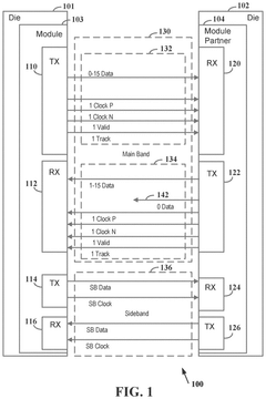
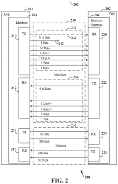
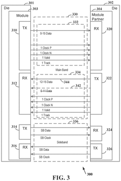
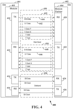
Variable link width in two directions for main band chip module connection
PatentPendingUS20240354279A1
Innovation
- Implementing a method to establish a die-to-die connection with a variable link width, allowing for independent configuration of transmit and receive data lanes through a sideband communication, enabling operation with different numbers of active data lanes in each direction to optimize power usage and data rates, and supporting fault tolerance by excluding faulty lines.
Die-to-die interconnect
PatentPendingCN117651940A
Innovation
- Using the Universal Chiplet Interconnect Express (UCIe) protocol, this protocol provides a universal, open on-package interconnect standard that supports high bandwidth, low latency and high power efficiency inter-core connections through standardized dies to The die interface enables interoperability across suppliers and factories.
Economic Impact and ROI Analysis of UCIe Adoption
The adoption of Universal Chiplet Interconnect Express (UCIe) represents a significant economic opportunity for the semiconductor industry. Initial financial projections indicate that companies implementing UCIe technology can expect a return on investment (ROI) ranging from 15% to 25% over a three-year period, primarily through reduced development costs and accelerated time-to-market for new products.
Cost reduction emerges as a primary economic benefit of UCIe adoption. Traditional monolithic chip designs require substantial non-recurring engineering (NRE) costs, often exceeding $500 million for advanced nodes. UCIe's chiplet approach enables companies to reuse existing IP blocks, potentially reducing development costs by 30-40% compared to traditional SoC designs. Additionally, manufacturing yields improve significantly when producing smaller chiplets versus large monolithic dies, translating to approximately 15-20% lower production costs.
Time-to-market advantages provide another substantial economic benefit. Industry analysis suggests UCIe-based designs can reduce development cycles by 4-6 months compared to traditional approaches. This acceleration creates competitive advantages and extends product revenue lifecycles, with early market entrants potentially capturing 10-15% additional market share in rapidly evolving segments like AI accelerators and data center processors.
The ecosystem economics of UCIe adoption present compelling opportunities for various industry participants. For foundries, UCIe enables more efficient capacity utilization and diversification of manufacturing processes. IP providers gain expanded markets through chiplet-based licensing models. System integrators benefit from more flexible supply chains and reduced dependency on single-source components, potentially reducing supply chain costs by 10-15% over time.
Long-term economic impacts extend beyond immediate cost savings. UCIe adoption enables more specialized and optimized designs, potentially improving performance-per-watt by 25-30% compared to equivalent monolithic implementations. This efficiency translates to operational cost savings for end users, particularly in data center environments where energy consumption represents a significant expense. Conservative estimates suggest a 3-year total cost of ownership (TCO) reduction of 12-18% for systems utilizing UCIe-based components.
Risk-adjusted ROI calculations must account for transition costs, including tooling investments, workforce training, and potential initial yield challenges. However, sensitivity analysis indicates that even with conservative assumptions, the economic benefits of UCIe adoption outweigh these transition costs within 18-24 months for most semiconductor companies actively engaged in advanced node development.
Interoperability and Standardization Roadmap
The UCIe (Universal Chiplet Interconnect Express) standardization roadmap represents a critical evolution in the semiconductor industry's approach to chiplet-based designs. The consortium behind UCIe, which includes industry giants like Intel, AMD, Arm, TSMC, and Samsung, has established a comprehensive framework for ensuring interoperability across different vendors' chiplets.
The standardization process began with the release of UCIe 1.0 specification in March 2022, focusing on die-to-die interconnect across package substrates. This initial specification defined two primary protocols: Standard and Advanced, with the former targeting lower bandwidth applications and the latter addressing high-performance computing needs.
Moving forward, the UCIe roadmap emphasizes three key standardization pillars: physical layer specifications, protocol layer definitions, and compliance testing methodologies. The physical layer standards address signal integrity, power delivery, and thermal considerations across different packaging technologies. Protocol standards ensure seamless communication between heterogeneous chiplets, while compliance testing frameworks verify adherence to the specification.
Industry adoption is progressing through a phased approach. The initial phase focuses on establishing basic interoperability between chiplets from different vendors within the same package. The intermediate phase aims to expand compatibility across different packaging technologies and manufacturing processes. The long-term vision targets plug-and-play functionality where chiplets from any consortium member can work together without custom integration efforts.
The roadmap also addresses critical challenges in testing and verification. The consortium is developing standardized test methodologies, reference designs, and certification processes to ensure chiplets meet the interoperability requirements. This includes the creation of compliance test suites and validation tools that manufacturers can use to verify their implementations.
Security and intellectual property protection represent another crucial aspect of the standardization roadmap. The consortium is working on frameworks for secure chiplet authentication, trusted execution environments, and IP protection mechanisms that allow vendors to safeguard their proprietary technologies while participating in the open ecosystem.
Looking ahead, the UCIe roadmap anticipates expansion beyond current use cases to include specialized domains such as AI accelerators, networking infrastructure, and automotive applications. Each domain will require specific extensions to the base specification while maintaining backward compatibility with the core standard.
Unlock deeper insights with Patsnap Eureka Quick Research — get a full tech report to explore trends and direct your research. Try now!
Generate Your Research Report Instantly with AI Agent
Supercharge your innovation with Patsnap Eureka AI Agent Platform!