

Advanced Substrate Materials For UCIe Chiplet Interconnect
SEP 1, 20259 MIN READ
Generate Your Research Report Instantly with AI Agent
Patsnap Eureka helps you evaluate technical feasibility & market potential.
UCIe Chiplet Interconnect Background and Objectives
Universal Chiplet Interconnect Express (UCIe) represents a significant advancement in semiconductor integration technology, emerging as a response to the increasing challenges of traditional monolithic chip scaling. The evolution of semiconductor technology has historically followed Moore's Law, but as physical limitations have become more pronounced, the industry has shifted towards chiplet-based architectures. UCIe was introduced in 2022 as an open industry standard to facilitate high-speed, low-latency connections between multiple chiplets within a package.
The development of UCIe builds upon previous interconnect technologies such as Intel's EMIB (Embedded Multi-die Interconnect Bridge) and AMD's Infinity Fabric, but with a crucial distinction: it aims to establish a universal standard that enables interoperability across different vendors' chiplets. This represents a paradigm shift from proprietary solutions to an ecosystem-based approach, potentially revolutionizing semiconductor design and manufacturing processes.
The primary technical objective of UCIe is to provide a standardized die-to-die interconnect that supports both package-level integration (within a single package) and board-level integration (across multiple packages). The standard encompasses physical layer specifications, protocol stack definitions, and compliance testing methodologies to ensure consistent performance and reliability across implementations.
UCIe technology targets data rates of up to 32 GT/s (giga-transfers per second) in its initial specification, with a roadmap for higher bandwidth in future iterations. This high-speed communication capability is essential for applications requiring intensive data exchange between computational units, such as artificial intelligence accelerators, high-performance computing systems, and data center infrastructure.
A critical aspect of UCIe's evolution is the development of advanced substrate materials that can support these high-speed interconnects. Traditional organic substrates face limitations in terms of signal integrity, thermal management, and mechanical stability at the fine pitches required for chiplet integration. This has driven research into novel substrate materials and architectures that can accommodate the demanding requirements of UCIe implementations.
The technological trajectory for UCIe includes not only improvements in bandwidth and latency but also advancements in power efficiency, as energy consumption becomes increasingly critical in modern computing systems. The standard aims to achieve a balance between performance and power consumption, making it suitable for a wide range of applications from mobile devices to data centers.
As the semiconductor industry continues to embrace heterogeneous integration, UCIe stands as a pivotal technology that could determine the future direction of chip design and manufacturing. Its success depends significantly on the development of appropriate substrate materials that can support the electrical, thermal, and mechanical requirements of high-density chiplet interconnections.
Market Analysis for Advanced Substrate Materials
The global market for advanced substrate materials for UCIe chiplet interconnect is experiencing robust growth, driven by the increasing demand for high-performance computing, artificial intelligence, and data center applications. The market size for advanced substrate materials is projected to reach $3.5 billion by 2027, growing at a CAGR of 14.2% from 2022 to 2027. This growth is primarily attributed to the rising adoption of heterogeneous integration technologies and the need for more efficient and compact computing solutions.
The demand for advanced substrate materials is particularly strong in regions with established semiconductor manufacturing ecosystems, including North America, East Asia (Taiwan, South Korea, Japan), and Europe. North America leads in terms of innovation and research, while East Asia dominates in manufacturing capacity and supply chain integration. Europe is emerging as a significant player due to recent initiatives to strengthen semiconductor sovereignty.
Market segmentation reveals distinct categories based on material types, with organic substrates holding approximately 45% market share, followed by ceramic substrates at 30% and silicon interposers at 25%. The organic substrate segment is growing fastest due to its cost-effectiveness and improving performance characteristics, making it suitable for mainstream chiplet integration applications.
End-user industry analysis shows that data centers and cloud service providers constitute the largest market segment (38%), followed by consumer electronics (27%), telecommunications (18%), automotive (12%), and others (5%). The data center segment's dominance is expected to continue as hyperscalers invest heavily in AI infrastructure requiring advanced chiplet-based architectures.
Key market drivers include the slowdown of Moore's Law, which has pushed the industry toward chiplet-based designs as an alternative scaling path. Additionally, the need for specialized computing solutions for AI workloads has accelerated the adoption of heterogeneous integration technologies that rely on advanced substrate materials. The push for more energy-efficient computing solutions also favors chiplet architectures that can optimize performance per watt.
Market challenges include high initial investment costs for new substrate technologies, supply chain vulnerabilities exposed during recent global disruptions, and technical challenges related to thermal management and signal integrity at increasingly fine interconnect pitches. These challenges are creating entry barriers but also opportunities for innovation.
The competitive landscape features established materials suppliers like Ibiden, Unimicron, and Shinko Electric, alongside new entrants focusing on novel substrate technologies specifically optimized for chiplet integration. Strategic partnerships between substrate manufacturers and semiconductor companies are becoming increasingly common as the ecosystem matures and standardization efforts around UCIe gain momentum.
Current Substrate Technologies and Challenges
The current substrate landscape for UCIe (Universal Chiplet Interconnect Express) implementation is dominated by organic substrates, primarily built on FR-4 and modified epoxy resin systems. These materials have served the semiconductor industry adequately for conventional packaging but face significant limitations when applied to the high-density interconnects required by chiplet architectures. Traditional organic substrates typically achieve line/space dimensions of 10/10μm at best, which increasingly constrains the routing density needed for advanced chiplet integration.
High-performance ceramic substrates, particularly those based on aluminum nitride (AlN) and aluminum oxide (Al2O3), offer superior thermal conductivity (170-230 W/m·K for AlN versus 0.3-0.5 W/m·K for organics) and dimensional stability. However, their widespread adoption remains limited due to substantially higher manufacturing costs and challenges in achieving the ultra-fine feature sizes required for UCIe implementations.
Glass substrates represent an emerging alternative with promising electrical properties, including lower dielectric constants (4.0-5.0) and loss tangents (0.001-0.005) compared to conventional organics. These characteristics enable higher signal integrity at the multi-GHz frequencies utilized in UCIe interfaces. Additionally, glass offers exceptional dimensional stability with coefficient of thermal expansion (CTE) values of 3-5 ppm/°C, closely matching silicon's 2.6 ppm/°C, which reduces thermomechanical stress at interconnection points.
The primary technical challenges facing substrate technologies for UCIe implementation include achieving the required fine-pitch interconnects (sub-5μm line/space) while maintaining manufacturing yield and reliability. Current photolithography and laser drilling processes struggle to consistently produce the high-density through-vias and traces needed for efficient chiplet-to-chiplet communication at scale. Additionally, warpage control becomes increasingly critical as substrate thicknesses decrease to accommodate shorter interconnect lengths.
Signal integrity presents another significant challenge, with cross-talk and impedance control becoming more difficult as interconnect density increases. The industry is exploring advanced dielectric materials with engineered electromagnetic properties to address these issues, including polymer composites with ceramic fillers that balance processability with electrical performance.
Thermal management remains a persistent challenge, particularly for high-performance computing applications where chiplets may generate significant heat flux. Current substrate materials often create thermal bottlenecks, necessitating the development of heterogeneous substrate architectures that incorporate localized high-conductivity pathways while maintaining overall electrical performance and manufacturing feasibility.
Current Advanced Substrate Solutions for UCIe
01 Advanced semiconductor substrate materials
Semiconductor substrates have evolved to include advanced materials that enhance electronic device performance. These materials include silicon-based compounds with improved electrical properties, compound semiconductors for high-frequency applications, and engineered substrates with specialized layers. These advanced substrate materials enable the development of more efficient and powerful electronic components while addressing challenges related to heat dissipation and electrical interference.- Silicon-based substrate materials for semiconductor applications: Advanced silicon-based substrate materials are widely used in semiconductor manufacturing due to their excellent electrical properties and compatibility with existing fabrication processes. These materials include modified silicon wafers, silicon-on-insulator (SOI) structures, and silicon carbide substrates that offer improved thermal conductivity, reduced leakage current, and enhanced device performance. These substrates serve as the foundation for various electronic components including integrated circuits and power devices.
- Ceramic and glass substrate materials for electronic applications: Ceramic and glass-based substrate materials provide excellent thermal stability, electrical insulation, and mechanical strength for various electronic applications. These materials include aluminum nitride, aluminum oxide, and specialized glass compositions that can withstand high processing temperatures while maintaining dimensional stability. They are particularly valuable in applications requiring high thermal conductivity, low dielectric loss, and resistance to harsh environmental conditions.
- Flexible and polymer-based substrate materials: Flexible and polymer-based substrate materials enable the development of bendable, lightweight electronic devices. These substrates incorporate advanced polymers, polyimides, and composite materials that maintain electrical performance while allowing for mechanical flexibility. They support applications in wearable electronics, flexible displays, and conformal sensors where traditional rigid substrates would be unsuitable. These materials often feature specialized surface treatments to enhance adhesion and electrical connectivity.
- Advanced substrate materials for power electronics: Specialized substrate materials for power electronic applications focus on enhanced thermal management and electrical isolation properties. These include direct bonded copper (DBC) substrates, insulated metal substrates (IMS), and advanced ceramic composites that can handle high power densities and operating temperatures. The materials feature optimized thermal expansion coefficients to reduce stress during thermal cycling and specialized metallization layers for improved electrical connectivity and heat dissipation.
- Nanomaterial-enhanced substrate technologies: Incorporation of nanomaterials into substrate compositions represents a cutting-edge approach to enhancing substrate performance. These advanced materials utilize carbon nanotubes, graphene, and other nanoscale additives to improve thermal conductivity, mechanical strength, and electrical properties. The nanomaterial-enhanced substrates enable miniaturization of electronic components while maintaining or improving performance characteristics. These technologies allow for novel device architectures and improved reliability in extreme operating conditions.
02 Composite substrate materials for improved durability
Composite substrate materials combine different materials to achieve enhanced durability and performance characteristics. These composites often incorporate reinforcing elements such as fibers, particles, or layered structures to improve mechanical strength, thermal stability, and resistance to environmental factors. The strategic combination of materials creates substrates with superior properties compared to single-material alternatives, making them suitable for demanding applications in various industries.Expand Specific Solutions03 Biodegradable and sustainable substrate materials
Environmentally friendly substrate materials derived from renewable resources offer sustainable alternatives to traditional materials. These biodegradable substrates incorporate natural fibers, plant-based polymers, and recycled components that reduce environmental impact while maintaining necessary performance characteristics. The development of these materials addresses growing concerns about waste management and resource conservation while meeting industry requirements for functionality and cost-effectiveness.Expand Specific Solutions04 Ceramic and glass-based advanced substrate materials
Advanced ceramic and glass-based substrates provide exceptional thermal stability and electrical insulation properties for specialized applications. These materials can withstand extreme temperatures, resist chemical degradation, and offer precise dimensional stability. Innovations in ceramic processing techniques have enabled the development of substrates with customized porosity, surface characteristics, and mechanical properties tailored for specific industrial requirements.Expand Specific Solutions05 Flexible and stretchable substrate materials
Flexible substrate materials enable the development of bendable, foldable, and stretchable electronic devices. These substrates incorporate polymers, thin films, and specialized composites that maintain functionality while undergoing mechanical deformation. The advancement of these materials has opened new possibilities for wearable technology, flexible displays, and conformable sensors that can adapt to irregular surfaces and dynamic environments.Expand Specific Solutions
Leading Companies in Advanced Substrate Industry
The UCIe chiplet interconnect substrate materials market is in a growth phase, with increasing demand driven by advanced packaging needs in high-performance computing. The market is expanding rapidly as chiplet technology becomes essential for overcoming traditional silicon scaling limitations. Leading semiconductor manufacturers like TSMC, Intel, and GlobalFoundries are investing heavily in advanced substrate technologies, with Intel's foundry services particularly focused on UCIe implementation. Materials innovation is occurring across various technology readiness levels, with Applied Materials, Corning, and NXP developing specialized substrate solutions. Asian players including Huawei and Win Semiconductors are accelerating R&D efforts, while established companies like IBM and Texas Instruments are leveraging their expertise to enhance substrate performance for next-generation chiplet integration.
Taiwan Semiconductor Manufacturing Co., Ltd.
Technical Solution: TSMC has developed advanced substrate materials specifically optimized for UCIe (Universal Chiplet Interconnect Express) implementation. Their approach focuses on high-density organic substrates with ultra-fine line/space capabilities (sub-2μm) that enable the high bandwidth density required by UCIe interfaces. TSMC's InFO_oS (Integrated Fan-Out on Substrate) technology serves as a bridge between chiplets and the organic substrate, providing enhanced electrical performance with reduced parasitic effects. The company has implemented specialized dielectric materials with low dielectric constants (Dk<3.0) and loss tangents (Df<0.002) to minimize signal integrity issues at the high frequencies (up to 16GHz) used in UCIe links. TSMC has also developed proprietary thermal interface materials that address the increased thermal challenges of densely packed chiplet designs, allowing for efficient heat dissipation from multiple dies. Their substrate solutions incorporate embedded capacitors and resistors to improve power delivery and signal integrity for UCIe implementations.
Strengths: Industry-leading process technology enabling the finest interconnect pitches; vertical integration capabilities allowing optimization across chip, package, and substrate; extensive experience with heterogeneous integration. Weaknesses: Higher cost compared to traditional substrate solutions; potential supply chain constraints during high demand periods; proprietary nature of some technologies may limit broader ecosystem adoption.
Intel Corp.
Technical Solution: Intel has pioneered advanced substrate materials for UCIe chiplet interconnect through their EMIB (Embedded Multi-die Interconnect Bridge) and Foveros technologies. For UCIe implementation, Intel has developed specialized organic substrates with embedded silicon bridges that provide high-density interconnects between chiplets. Their substrates feature ultra-fine pitch capabilities (down to 25μm) with specialized low-loss dielectric materials optimized for the 16GT/s data rates specified in UCIe standards. Intel's approach includes advanced RDL (redistribution layer) technology with copper traces as thin as 2μm to minimize electrical parasitics. The company has also implemented novel thermal management solutions within their substrates, including integrated microfluidic channels and high thermal conductivity materials (>20 W/m·K) to address the increased power density of multi-chiplet designs. Intel's substrate technology incorporates specialized power delivery networks with embedded capacitors to manage the power requirements of high-performance chiplets while maintaining signal integrity across UCIe interfaces.
Strengths: Extensive experience with heterogeneous integration technologies; proven manufacturing capabilities at scale; strong influence on UCIe standards development as a founding member. Weaknesses: Historically more focused on proprietary interconnect solutions which may affect UCIe implementation; higher manufacturing costs compared to traditional packaging; thermal management challenges with densely packed chiplets.
Key Innovations in Substrate Material Technologies
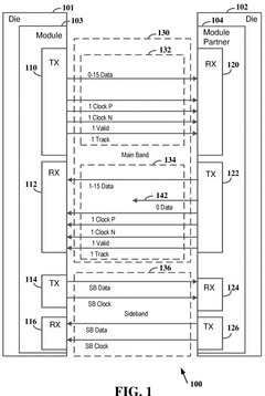
Electronic device
PatentPendingUS20240371781A1
Innovation
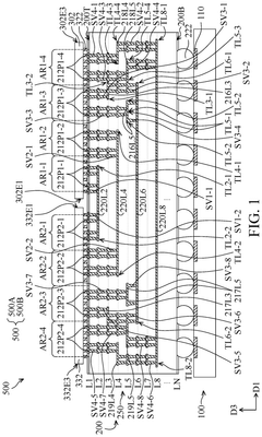
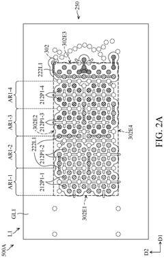
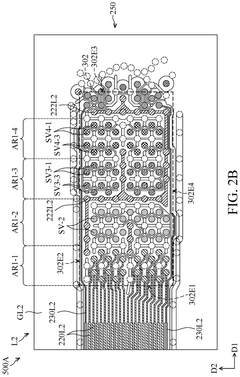
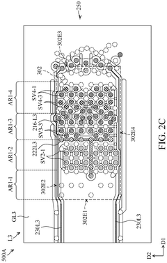
- The electronic device employs a substrate with an interconnect structure that includes misaligned via structures composed of fewer stacked vias, reducing fabrication complexity and cost, and is designed to ensure SI/PI performance by using additional signal traces and ground layers to improve signal and power integrity at deeper levels of the substrate.
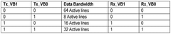
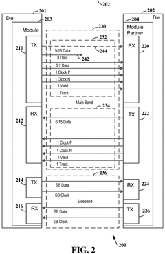
Variable link width in two directions for main band chip module connection
PatentWO2024226177A1
Innovation
- Implementing a variable link width mechanism in both directions of the main band connection, allowing for dynamic adjustment of the number of active data lanes based on requirements through a sideband communication protocol, enabling independent configuration of transmit and receive data lines to optimize power usage and data rates.

Supply Chain Considerations for Advanced Materials
The supply chain for advanced substrate materials in UCIe chiplet interconnect technology represents a critical component of the semiconductor ecosystem. The increasing complexity of these materials, particularly those required for high-density interconnects with fine pitch and high signal integrity, has created significant challenges in sourcing, manufacturing, and quality control processes.
Material sourcing for advanced substrates faces geographical concentration risks, with key raw materials such as high-purity copper, specialized polymers, and ceramic compounds predominantly produced in specific regions. This concentration creates potential vulnerabilities to geopolitical tensions, trade restrictions, and natural disasters. For instance, high-grade ABF (Ajinomoto Build-up Film) substrate materials are primarily manufactured in Japan, Taiwan, and South Korea, creating regional dependencies.
Manufacturing capacity constraints represent another significant challenge. The production of advanced substrate materials requires specialized equipment and expertise, with only a limited number of suppliers capable of meeting the stringent requirements for UCIe applications. This supply-demand imbalance has led to extended lead times, often exceeding 40-52 weeks for certain high-end substrate materials, creating potential bottlenecks in chiplet production schedules.
Quality control and consistency across the supply chain present additional complexities. Advanced substrate materials for UCIe must maintain extremely tight tolerances for warpage, planarity, and electrical performance. Ensuring consistent quality across multiple production batches and suppliers requires sophisticated testing methodologies and robust supplier qualification processes.
The environmental impact of advanced substrate production has also emerged as a supply chain consideration. Water usage, chemical handling, and energy consumption in substrate manufacturing have prompted increased regulatory scrutiny and sustainability requirements. Forward-thinking companies are developing more environmentally friendly substrate materials and manufacturing processes to address these concerns.
Vertical integration strategies are being adopted by some major semiconductor companies to mitigate supply chain risks. By investing in or acquiring substrate manufacturing capabilities, these companies aim to secure access to critical materials and reduce dependencies on external suppliers. This trend may reshape the competitive landscape of the substrate supply chain in the coming years.
Diversification of supplier networks has become a strategic imperative for companies implementing UCIe technology. Developing alternative sources for critical materials and qualifying multiple suppliers helps mitigate single-source risks while potentially improving cost structures through competitive bidding processes.
Thermal Management in UCIe Implementations
Thermal management represents a critical challenge in UCIe (Universal Chiplet Interconnect Express) implementations due to the high-density integration of multiple chiplets on advanced substrate materials. As chiplet architectures continue to evolve with increasing power densities and performance requirements, effective thermal solutions become essential for maintaining system reliability and performance.
The thermal challenges in UCIe implementations stem primarily from the concentrated heat generation at interconnect points between chiplets. These junction areas experience significant thermal stress due to the high-frequency signal transmission and power delivery requirements. Advanced substrate materials must therefore incorporate thermal management features that can efficiently dissipate heat while maintaining the electrical performance characteristics required for high-bandwidth die-to-die communications.
Current thermal management approaches in UCIe implementations include the integration of thermal interface materials (TIMs) with enhanced thermal conductivity properties. These materials are strategically placed between chiplets and heat spreaders to facilitate efficient heat transfer away from critical interconnect regions. Silicon-based TIMs with embedded metallic particles have shown promising results in recent implementations, offering thermal conductivity values exceeding 20 W/m·K while maintaining the mechanical compliance needed for reliable operation.
Active cooling solutions are increasingly being incorporated into advanced substrate designs for UCIe implementations. Microfluidic channels embedded within the substrate material provide targeted cooling to high-heat-flux areas, particularly around dense interconnect regions. These solutions have demonstrated the capability to manage heat loads exceeding 500 W/cm² in laboratory settings, though commercial implementations typically target the 200-300 W/cm² range.
Thermal simulation and modeling have become essential tools in the development of UCIe substrate materials. Multi-physics simulation approaches that simultaneously account for electrical, mechanical, and thermal behaviors enable designers to optimize substrate architectures for balanced performance. These tools have revealed that strategic placement of thermal vias and copper-filled through-silicon vias (TSVs) can reduce junction temperatures by up to 15°C in typical chiplet configurations.
Emerging approaches include the development of phase-change materials integrated directly into substrate structures. These materials can absorb significant thermal energy during phase transitions, effectively buffering temperature spikes during high-performance operation cycles. When combined with traditional passive and active cooling techniques, these advanced thermal management solutions enable the full performance potential of UCIe interconnect technologies while maintaining reliable thermal profiles.
Unlock deeper insights with Patsnap Eureka Quick Research — get a full tech report to explore trends and direct your research. Try now!
Generate Your Research Report Instantly with AI Agent
Supercharge your innovation with Patsnap Eureka AI Agent Platform!