Latency-Power-Area Tradeoffs For UCIe Chiplet Interconnect
SEP 1, 20259 MIN READ
Generate Your Research Report Instantly with AI Agent
Patsnap Eureka helps you evaluate technical feasibility & market potential.
UCIe Chiplet Interconnect Background and Objectives
Universal Chiplet Interconnect Express (UCIe) represents a pivotal advancement in semiconductor integration technology, emerging as a response to the increasing challenges of traditional monolithic chip scaling. The evolution of semiconductor technology has historically followed Moore's Law, with transistor density doubling approximately every two years. However, as process nodes have shrunk below 7nm, physical limitations and exponentially rising manufacturing costs have necessitated alternative approaches to continue performance scaling.
Chiplet architecture has emerged as a compelling solution, allowing complex systems to be disaggregated into smaller, specialized dies (chiplets) that can be manufactured using optimal process technologies and later integrated into a single package. This approach enables mixing of heterogeneous technologies, reduces manufacturing costs through improved yields, and facilitates more flexible product development cycles.
UCIe, introduced in March 2022 by an industry consortium including Intel, AMD, Arm, TSMC, Samsung, and others, aims to standardize chiplet interconnection across the industry. Prior to UCIe, chiplet integration relied on proprietary interconnect technologies such as Intel's EMIB, AMD's Infinity Fabric, and TSMC's CoWoS, creating ecosystem fragmentation and limiting interoperability between different vendors' chiplets.
The primary objective of UCIe is to establish an open, unified interconnect standard that enables chiplets from different vendors to seamlessly communicate within a package. UCIe 1.0 specification defines both the physical layer and protocol stack for die-to-die communication, supporting two primary modes: a standard package for general applications and an advanced package for high-performance computing scenarios.
UCIe technology targets three critical performance metrics: latency, power consumption, and silicon area utilization. These parameters form an interdependent triangle where optimizing one typically requires compromises in the others. For instance, reducing latency often demands more power, while minimizing area might increase latency or power consumption.
The technical goals of UCIe include achieving ultra-low latency communication between chiplets (sub-nanosecond range), minimizing power consumption to maintain thermal efficiency within densely packed multi-chiplet packages, and optimizing the silicon area dedicated to interconnect circuitry to maximize cost-effectiveness.
As system architects and semiconductor companies implement UCIe in their designs, understanding the fundamental tradeoffs between latency, power, and area becomes essential for optimizing chiplet-based systems for specific application requirements, whether prioritizing performance, energy efficiency, or cost-effectiveness.
Market Demand Analysis for Chiplet-Based Systems
The chiplet-based system market is experiencing unprecedented growth, driven by the increasing demand for high-performance computing solutions across various industries. As traditional monolithic chip designs reach their physical and economic limits, chiplet technology has emerged as a viable alternative, offering improved scalability, flexibility, and cost-effectiveness. The Universal Chiplet Interconnect Express (UCIe) standard represents a significant advancement in this domain, providing a standardized approach to chiplet integration.
Market research indicates that the global chiplet market is projected to grow at a compound annual growth rate of over 40% from 2023 to 2030. This explosive growth is primarily fueled by data centers, artificial intelligence applications, and high-performance computing sectors, which collectively demand more powerful and efficient computing solutions. The need for reduced latency, optimized power consumption, and efficient area utilization has become paramount in these applications.
Data centers, in particular, are experiencing a paradigm shift toward disaggregated architectures, where computing resources are distributed across multiple specialized chiplets rather than concentrated in monolithic designs. This trend is driven by the need for more efficient resource utilization and the ability to scale specific components independently. UCIe-based chiplet interconnects are positioned to address these requirements by enabling seamless integration of heterogeneous chiplets.
The artificial intelligence and machine learning sectors represent another significant market segment for chiplet-based systems. These applications require massive parallel processing capabilities and memory bandwidth, which can be efficiently delivered through specialized chiplets interconnected via UCIe. The market demand in this segment is expected to grow substantially as AI applications become more pervasive across industries.
Consumer electronics manufacturers are also showing increased interest in chiplet technology, particularly for high-end devices requiring superior performance within constrained power and thermal envelopes. The ability to mix and match chiplets from different process nodes and vendors offers unprecedented flexibility in product design and differentiation.
From a geographical perspective, North America currently leads the chiplet market, followed by Asia-Pacific and Europe. However, the Asia-Pacific region is expected to witness the highest growth rate due to the strong presence of semiconductor manufacturing facilities and increasing investments in advanced computing technologies.
The market demand for chiplet-based systems is further amplified by the semiconductor industry's ongoing challenges, including the slowdown of Moore's Law and rising fabrication costs for advanced process nodes. These factors make the chiplet approach increasingly attractive as it allows for more cost-effective utilization of cutting-edge process technologies while maintaining backward compatibility with mature nodes for less critical components.
UCIe Technical Challenges and Current Limitations
UCIe (Universal Chiplet Interconnect Express) faces several significant technical challenges that impact its implementation and performance. The primary challenge lies in balancing the critical tradeoffs between latency, power consumption, and silicon area. As chiplet designs become more complex, maintaining low latency becomes increasingly difficult, especially when signals must traverse multiple die boundaries. Current UCIe implementations struggle to achieve sub-10ns latencies in complex multi-chiplet configurations, which can become a bottleneck for latency-sensitive applications.
Power efficiency presents another major limitation. The PHY layer of UCIe consumes substantial power during high-bandwidth data transfers, with current implementations requiring 1-2 pJ/bit. This power consumption becomes particularly problematic in dense chiplet configurations where thermal constraints are already challenging. The SerDes circuits used for high-speed communication are especially power-hungry, creating thermal hotspots that can affect overall system reliability.
Area constraints further complicate UCIe implementation. The die-to-die (D2D) interfaces require significant silicon real estate for PHY circuitry, including SerDes, equalization circuits, and clock recovery systems. Current UCIe implementations typically require 0.2-0.5 mm² per channel, which can consume up to 10-15% of the die area in smaller chiplets. This area overhead directly impacts manufacturing costs and limits the minimum viable size for chiplets.
Signal integrity issues represent another critical challenge. As data rates increase beyond 16 GT/s, maintaining signal integrity across package substrates becomes increasingly difficult. Current UCIe implementations struggle with crosstalk, impedance matching, and power supply noise at higher frequencies, limiting the practical bandwidth density that can be achieved.
Testing and validation of UCIe interfaces present unique challenges compared to traditional monolithic designs. The current lack of standardized test methodologies for chiplet interfaces makes it difficult to ensure interoperability between chiplets from different vendors. Known-good-die testing becomes more complex when the functionality depends on high-speed interfaces that cannot be fully tested before assembly.
Manufacturing variability also impacts UCIe performance. Process variations between different chiplets can lead to timing mismatches and signal integrity issues. Current UCIe implementations have limited ability to adapt to these variations, requiring conservative design margins that reduce overall performance.
Lastly, thermal management across the chiplet interface presents significant challenges. The high-density interconnects create thermal barriers that complicate heat dissipation. Current cooling solutions struggle to effectively manage hotspots at chiplet boundaries, potentially limiting the maximum sustainable bandwidth of UCIe interfaces in thermally constrained environments.
Current Latency-Power-Area Optimization Approaches
01 UCIe chiplet interconnect architecture for latency optimization
The Universal Chiplet Interconnect Express (UCIe) architecture provides optimized interconnect solutions between chiplets, focusing on reducing latency in multi-die systems. This architecture implements advanced routing techniques, buffer management, and protocol optimizations to minimize communication delays between chiplets. The design includes specialized physical layer implementations that support high-speed data transfer while maintaining signal integrity across die boundaries, enabling efficient communication between heterogeneous chiplets in advanced packaging configurations.- UCIe architecture for optimizing latency in chiplet interconnects: The Universal Chiplet Interconnect Express (UCIe) architecture provides specific design approaches to minimize latency in chiplet-to-chiplet communications. These include optimized physical layer protocols, reduced hop counts between chiplets, and specialized routing techniques. The architecture implements low-latency communication channels that support both die-to-die and package-to-package connections, enabling high-speed data transfer with minimal delay for complex computing systems.
- Power efficiency techniques in UCIe chiplet designs: Various power management techniques are employed in UCIe chiplet interconnect designs to optimize energy consumption. These include dynamic voltage and frequency scaling, power gating for inactive components, and specialized low-power states for different operating conditions. Advanced power delivery networks are implemented to ensure efficient power distribution across multiple chiplets while maintaining signal integrity. These techniques collectively reduce overall system power consumption while maintaining high performance levels.
- Area optimization strategies for UCIe implementations: Area optimization in UCIe chiplet interconnects focuses on efficient use of silicon real estate through advanced packaging technologies and interconnect designs. Techniques include microbump array optimization, reduced PHY footprints, and efficient bump pitch designs. The architecture supports high-density connections between chiplets while minimizing the overall package size. These approaches enable more functional components to be integrated into smaller form factors, supporting the development of more compact and powerful computing systems.
- UCIe protocol layers and performance optimization: The UCIe specification defines multiple protocol layers that work together to optimize chiplet interconnect performance. These layers include the physical layer, data link layer, transaction layer, and protocol adaptation layers. Each layer implements specific optimizations for bandwidth, latency, and reliability. The architecture supports various protocols including PCIe, CXL, and custom protocols, allowing flexibility in chiplet design while maintaining standardized interfaces. This layered approach enables scalable performance across different chiplet configurations.
- Testing and validation methodologies for UCIe interconnects: Specialized testing and validation methodologies are critical for ensuring UCIe chiplet interconnect performance meets specifications for latency, power, and area. These include high-speed signal integrity testing, power integrity analysis, thermal validation, and interoperability testing between chiplets from different vendors. Advanced test structures are integrated into chiplet designs to facilitate both manufacturing testing and in-field diagnostics. These methodologies help identify and resolve issues related to signal quality, power distribution, and thermal management in multi-chiplet systems.
02 Power efficiency techniques in UCIe chiplet designs
Various power management techniques are employed in UCIe chiplet interconnect implementations to optimize energy consumption. These include dynamic voltage and frequency scaling, power gating for inactive interconnect lanes, and adaptive power states based on bandwidth requirements. The interconnect design incorporates low-power physical layer circuits, energy-efficient serialization/deserialization mechanisms, and optimized clock distribution networks. These techniques collectively reduce power consumption while maintaining the required performance levels for high-speed die-to-die communication.Expand Specific Solutions03 Area optimization strategies for UCIe implementation
Area efficiency is critical in UCIe chiplet interconnect designs, with several approaches to minimize silicon footprint. These include compact physical interface designs, optimized bump patterns for die-to-die connections, and efficient circuit layouts for transceivers and PHY components. The architecture employs shared resources where possible, uses advanced process nodes for interface logic, and implements area-efficient serialization techniques. These strategies help reduce the overall silicon area dedicated to interconnect functionality while maintaining the required bandwidth and signal integrity.Expand Specific Solutions04 Performance and reliability enhancements in UCIe
UCIe chiplet interconnect incorporates various features to enhance performance and reliability. These include error detection and correction mechanisms, retry protocols for failed transmissions, and link training procedures to optimize signal quality. Advanced equalization techniques compensate for channel impairments, while adaptive tuning mechanisms optimize performance under varying operating conditions. The architecture also supports redundancy features and graceful degradation modes to maintain system operation even when partial failures occur in the interconnect fabric.Expand Specific Solutions05 Integration and compatibility features of UCIe
UCIe chiplet interconnect technology provides extensive integration and compatibility features to support heterogeneous chiplet ecosystems. The architecture defines standardized interfaces that enable interoperability between chiplets from different vendors and process technologies. It supports various packaging technologies including silicon interposers, organic substrates, and advanced bridge technologies. The specification includes protocol adaptation layers to bridge between different interface standards, enabling seamless integration of diverse IP blocks while maintaining the latency, power, and area benefits of the UCIe architecture.Expand Specific Solutions
Key Industry Players in Chiplet Ecosystem
The UCIe chiplet interconnect technology market is currently in its early growth phase, characterized by significant investments from major semiconductor players. The market is expanding rapidly as chiplet-based designs become essential for addressing power and performance challenges in advanced computing systems. Key competitors including Intel, TSMC, Qualcomm, and Samsung are driving innovation in this space, focusing on optimizing the critical latency-power-area tradeoffs. These companies are developing proprietary solutions while participating in the UCIe consortium to establish industry standards. Chinese entities like Huawei and research institutions are also making strategic investments to reduce dependency on Western technology. The market is expected to grow substantially as chiplet architectures become fundamental to next-generation computing systems, with technical maturity varying across implementations but advancing rapidly through collaborative industry efforts.
QUALCOMM, Inc.
Technical Solution: Qualcomm has developed a UCIe implementation strategy focused on mobile and edge computing applications, where power efficiency is paramount. Their approach leverages their expertise in system-on-chip design to optimize the latency-power-area tradeoffs for battery-powered devices. Qualcomm's UCIe solution incorporates their proprietary FlexLink D2D interconnect technology, which achieves data rates of up to 20 GT/s while maintaining ultra-low power consumption (approximately 0.4 pJ/bit). Their implementation includes adaptive power management features that can dynamically adjust link width, frequency, and voltage based on bandwidth requirements. Qualcomm has optimized their PHY design to minimize area overhead, achieving interconnect densities of over 1000 connections per mm². Their architecture supports both cache-coherent and non-coherent protocols, with specialized optimizations for AI accelerator integration. Qualcomm's UCIe implementation includes sophisticated error detection and correction mechanisms while maintaining latencies under 2ns for die-to-die communication, making it suitable for real-time applications.
Strengths: Industry-leading power efficiency optimized for mobile applications; extensive experience with heterogeneous computing architectures; proven track record in high-volume chiplet production. Weaknesses: More focused on mobile/edge use cases with potentially fewer optimizations for data center applications; proprietary extensions may limit interoperability with other vendors' chiplets; relatively newer entrant to the high-performance computing market compared to Intel.
Intel Corp.
Technical Solution: Intel has pioneered UCIe (Universal Chiplet Interconnect Express) technology as a founding member of the UCIe consortium. Their approach focuses on optimizing the latency-power-area tradeoffs through their Advanced Interface Bus (AIB) technology, which serves as a foundation for UCIe. Intel's implementation utilizes die-to-die (D2D) PHY technology that supports both standard and advanced packaging options. Their solution achieves data rates of up to 16 GT/s while maintaining power efficiency through adaptive voltage scaling and multiple power states. Intel has implemented sophisticated clock domain crossing techniques and optimized physical layer designs that reduce latency to sub-nanosecond levels for die-to-die communication. Their architecture supports both parallel and serial interfaces with configurable lane widths to address different bandwidth and area requirements. Intel's UCIe implementation includes built-in error correction capabilities and supports both synchronous and asynchronous communication modes to optimize for different use cases.
Strengths: Industry-leading expertise in chiplet design with established ecosystem support; comprehensive IP portfolio for chiplet interconnects; advanced packaging technologies (EMIB, Foveros) that complement UCIe implementation. Weaknesses: Higher implementation complexity requiring sophisticated design tools; potential vendor lock-in with proprietary extensions to the UCIe standard; higher initial design costs compared to monolithic approaches.
Critical Patents and Research in UCIe Implementation
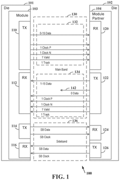
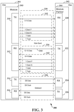
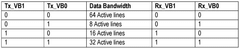
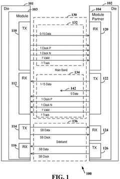
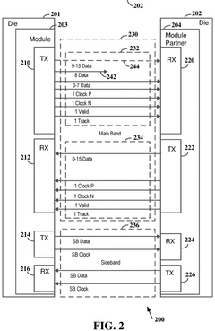
Variable link width in two directions for main band chip module connection
PatentPendingUS20240354279A1
Innovation
- Implementing a method to establish a die-to-die connection with a variable link width, allowing for independent configuration of transmit and receive data lanes through a sideband communication, enabling operation with different numbers of active data lanes in each direction to optimize power usage and data rates, and supporting fault tolerance by excluding faulty lines.
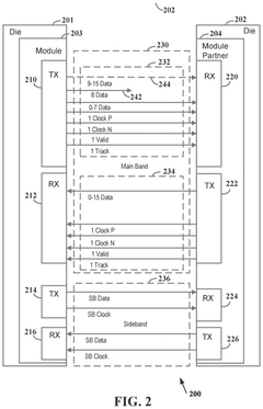
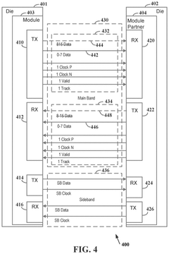
Variable link width in two directions for main band chip module connection
PatentWO2024226177A1
Innovation
- Implementing a variable link width mechanism in both directions of the main band connection, allowing for dynamic adjustment of the number of active data lanes based on requirements through a sideband communication protocol, enabling independent configuration of transmit and receive data lines to optimize power usage and data rates.

Thermal Management Strategies for Chiplet Designs
Thermal management has become a critical challenge in chiplet-based designs, particularly for UCIe (Universal Chiplet Interconnect Express) implementations where latency, power, and area considerations intersect with thermal constraints. As chiplet architectures pack more computing power into smaller spaces, heat dissipation emerges as a limiting factor that directly impacts performance, reliability, and energy efficiency.
The thermal challenges in UCIe chiplet interconnects stem from several factors. First, the high-density interconnects between chiplets create localized hotspots that can exceed thermal design power (TDP) limits. These hotspots are particularly problematic at the interface boundaries where signal integrity must be maintained despite thermal gradients. Second, the heterogeneous nature of chiplet designs means varying thermal profiles across different functional units, complicating uniform cooling approaches.
Current thermal management strategies for UCIe implementations include both passive and active cooling techniques. Passive approaches focus on optimized package designs with enhanced thermal interface materials (TIMs) that improve heat transfer between chiplets and heat spreaders. Advanced TIMs with higher thermal conductivity are being developed specifically for chiplet applications, offering up to 40% improvement in heat dissipation compared to conventional materials.
Active cooling solutions incorporate microfluidic channels integrated directly into interposer layers, enabling targeted cooling of high-power chiplets. These solutions have demonstrated the ability to handle thermal densities exceeding 500W/cm², which is critical for high-performance computing applications utilizing UCIe interconnects. Additionally, dynamic thermal management (DTM) techniques that adjust clock frequencies and voltage levels based on real-time thermal monitoring help maintain optimal operating conditions.
The industry is also exploring novel approaches such as embedded vapor chambers within package substrates and phase-change materials that absorb heat during peak processing periods. These innovations aim to address the unique thermal challenges posed by the dense interconnect structures required for low-latency chiplet communication in UCIe implementations.
Thermal-aware design methodologies are increasingly important in the UCIe ecosystem, with EDA tools now incorporating thermal simulation capabilities that account for the complex power-performance-area tradeoffs. These tools enable designers to optimize chiplet placement and interconnect routing to minimize thermal hotspots while maintaining signal integrity and meeting latency requirements.
As UCIe adoption accelerates, thermal management will continue to evolve, with increasing focus on holistic cooling solutions that address system-level thermal constraints while enabling the performance benefits of chiplet architectures. The development of standardized thermal models and metrics specific to chiplet designs will be essential for comparing different cooling approaches and ensuring reliable operation across diverse application scenarios.
Standardization and Interoperability Considerations
The UCIe (Universal Chiplet Interconnect Express) standard represents a pivotal development in chiplet-based system design, establishing a framework for interoperability across different vendors and technologies. This standardization effort addresses the fragmentation that previously characterized the chiplet ecosystem, where proprietary interconnect solutions limited cross-vendor integration capabilities.
The UCIe Consortium, formed in 2022 with founding members including Intel, AMD, Arm, TSMC, and Samsung, has established a comprehensive specification covering physical layer, protocol stack, and software layers. This multi-layered approach ensures that chiplets from different manufacturers can communicate effectively while maintaining performance standards. The specification's hierarchical structure allows for innovation within defined parameters while preserving essential interoperability.
Interoperability testing and certification programs are emerging as critical components of the UCIe ecosystem. These programs validate compliance with the standard and ensure reliable operation across diverse implementations. The development of reference designs and validation suites by the consortium provides essential tools for manufacturers to verify their chiplet designs against the standard before market introduction.
The standard's evolution must balance competing interests: maintaining backward compatibility while incorporating technological advancements. The UCIe roadmap includes provisions for future enhancements in bandwidth, power efficiency, and latency reduction without compromising the fundamental interoperability promise. This forward-looking approach protects investments in UCIe-compliant designs.
Intellectual property considerations present both challenges and opportunities for the UCIe ecosystem. The consortium has established RAND (Reasonable and Non-Discriminatory) licensing terms for essential patents, creating a balanced framework that encourages participation while protecting innovation. This approach has facilitated broader adoption compared to previous interconnect technologies.
Regional standardization bodies, including IEEE, JEDEC, and various national standards organizations, are increasingly recognizing UCIe as a reference standard for chiplet interconnects. This global recognition strengthens the standard's position and encourages alignment of regional requirements with the UCIe specification, reducing market fragmentation and simplifying compliance for manufacturers operating in multiple regions.
The emergence of UCIe as a unifying standard has catalyzed the development of a more robust chiplet marketplace, where specialized components can be sourced from multiple vendors and integrated into high-performance systems with greater confidence in their interoperability and performance characteristics.
Unlock deeper insights with Patsnap Eureka Quick Research — get a full tech report to explore trends and direct your research. Try now!
Generate Your Research Report Instantly with AI Agent
Supercharge your innovation with Patsnap Eureka AI Agent Platform!