

UCIe Chiplet Interconnect Yield-Cost Sensitivity Models
SEP 1, 20259 MIN READ
Generate Your Research Report Instantly with AI Agent
Patsnap Eureka helps you evaluate technical feasibility & market potential.
UCIe Chiplet Technology Background and Objectives
The Universal Chiplet Interconnect Express (UCIe) represents a significant advancement in semiconductor integration technology, emerging as a response to the increasing challenges of traditional monolithic chip scaling. Developed through industry collaboration, UCIe aims to establish an open, standardized die-to-die interconnect technology that enables heterogeneous integration of chiplets from different vendors and process technologies.
The evolution of chiplet technology can be traced back to the slowdown of Moore's Law, where the traditional approach of shrinking transistors became increasingly difficult and costly. This limitation prompted the semiconductor industry to explore alternative integration strategies, leading to the development of multi-chip modules and eventually chiplet-based designs. UCIe builds upon previous interconnect technologies such as Intel's AIB (Advanced Interface Bus) and EMIB (Embedded Multi-die Interconnect Bridge), AMD's Infinity Fabric, and TSMC's CoWoS (Chip on Wafer on Substrate).
UCIe technology addresses several critical objectives in modern semiconductor design. Primarily, it seeks to enable cost-effective scaling by allowing designers to partition complex systems into smaller, more manufacturable chiplets. This approach potentially improves yield rates by reducing the die size of individual components, thereby decreasing the probability of fatal defects per die.
Another key objective of UCIe is to facilitate heterogeneous integration, allowing chiplets manufactured using different process nodes to be combined in a single package. This capability enables system designers to optimize performance, power, and cost by selecting the most appropriate process technology for each functional block.
The standardization aspect of UCIe represents a crucial industry milestone. By establishing common electrical and physical specifications for die-to-die interfaces, UCIe aims to create an ecosystem where chiplets from different vendors can interoperate seamlessly. This standardization is expected to foster innovation and competition in the chiplet market, potentially leading to reduced costs and accelerated technology development.
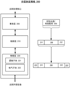
UCIe technology encompasses both package-level and silicon-level specifications. At the package level, it defines the physical and electrical characteristics of the interconnect, including bump pitch, power delivery, and thermal management. At the silicon level, it specifies protocols for data transfer, error handling, and power management, ensuring reliable communication between chiplets.
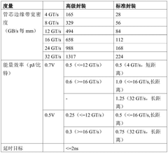
The technology trend indicates a progressive improvement in interconnect density, bandwidth, and energy efficiency. Current UCIe implementations support data rates of up to 32 GT/s, with roadmaps projecting significant increases in future generations. These advancements are critical for meeting the growing bandwidth demands of data-intensive applications such as artificial intelligence, high-performance computing, and advanced networking.
The evolution of chiplet technology can be traced back to the slowdown of Moore's Law, where the traditional approach of shrinking transistors became increasingly difficult and costly. This limitation prompted the semiconductor industry to explore alternative integration strategies, leading to the development of multi-chip modules and eventually chiplet-based designs. UCIe builds upon previous interconnect technologies such as Intel's AIB (Advanced Interface Bus) and EMIB (Embedded Multi-die Interconnect Bridge), AMD's Infinity Fabric, and TSMC's CoWoS (Chip on Wafer on Substrate).
UCIe technology addresses several critical objectives in modern semiconductor design. Primarily, it seeks to enable cost-effective scaling by allowing designers to partition complex systems into smaller, more manufacturable chiplets. This approach potentially improves yield rates by reducing the die size of individual components, thereby decreasing the probability of fatal defects per die.
Another key objective of UCIe is to facilitate heterogeneous integration, allowing chiplets manufactured using different process nodes to be combined in a single package. This capability enables system designers to optimize performance, power, and cost by selecting the most appropriate process technology for each functional block.
The standardization aspect of UCIe represents a crucial industry milestone. By establishing common electrical and physical specifications for die-to-die interfaces, UCIe aims to create an ecosystem where chiplets from different vendors can interoperate seamlessly. This standardization is expected to foster innovation and competition in the chiplet market, potentially leading to reduced costs and accelerated technology development.
UCIe technology encompasses both package-level and silicon-level specifications. At the package level, it defines the physical and electrical characteristics of the interconnect, including bump pitch, power delivery, and thermal management. At the silicon level, it specifies protocols for data transfer, error handling, and power management, ensuring reliable communication between chiplets.
The technology trend indicates a progressive improvement in interconnect density, bandwidth, and energy efficiency. Current UCIe implementations support data rates of up to 32 GT/s, with roadmaps projecting significant increases in future generations. These advancements are critical for meeting the growing bandwidth demands of data-intensive applications such as artificial intelligence, high-performance computing, and advanced networking.
Market Analysis for Chiplet-Based Integration Solutions
The chiplet-based integration market is experiencing rapid growth, driven by the increasing demand for high-performance computing solutions across various industries. Current market valuations place the global chiplet market at approximately 5.8 billion USD in 2023, with projections indicating a compound annual growth rate (CAGR) of 40% through 2030. This exceptional growth trajectory is primarily fueled by the semiconductor industry's shift away from traditional monolithic designs toward more modular and cost-effective chiplet architectures.
Key market segments demonstrating strong demand for chiplet-based solutions include data centers, artificial intelligence accelerators, high-performance computing, telecommunications infrastructure, and advanced consumer electronics. The data center segment currently represents the largest market share at roughly 38%, followed by AI accelerators at 27%. These segments particularly benefit from the performance advantages and cost efficiencies offered by UCIe-based chiplet integration.
From a regional perspective, North America leads the market with approximately 42% share, followed by Asia-Pacific at 36%, with Taiwan, South Korea, and China serving as manufacturing hubs. Europe accounts for about 18% of the market, with growing investments in chiplet technology development.
The market dynamics are significantly influenced by the yield-cost relationship in chiplet manufacturing. Industry analysis indicates that improving die yield by just 5% through optimized UCIe interconnect technologies can reduce overall production costs by 12-15%, representing substantial savings for high-volume manufacturers. This sensitivity between yield and cost is becoming a critical competitive differentiator in the market.
Customer demand patterns reveal a strong preference for solutions that offer flexibility in chiplet integration while maintaining high performance standards. Enterprise customers are willing to pay a premium of 15-20% for chiplet solutions that demonstrate superior reliability metrics and compatibility across different vendor ecosystems.
Market forecasts suggest that UCIe-compliant chiplet solutions will capture over 65% of the advanced packaging market by 2027, driven by the standardization benefits and ecosystem development. The yield-cost sensitivity models indicate that manufacturers achieving best-in-class interconnect yields can expect to gain 3-4% in market share annually, highlighting the strategic importance of yield optimization technologies in this rapidly evolving market landscape.
UCIe Interconnect Technical Challenges and Limitations
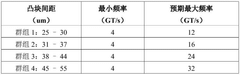
Despite the promising advancements in UCIe (Universal Chiplet Interconnect Express) technology, several significant technical challenges and limitations persist that impact yield and cost sensitivity models. The primary challenge lies in the ultra-fine pitch interconnects required for die-to-die communication, typically ranging from 25-55μm. At these dimensions, manufacturing precision becomes critically important, with even minor alignment errors potentially causing catastrophic connection failures.
Thermal management presents another substantial hurdle for UCIe implementations. The dense packaging of multiple chiplets creates concentrated heat zones that can lead to thermal gradients across the package. These temperature variations not only affect signal integrity but also accelerate electromigration and other reliability concerns, ultimately impacting the interconnect yield and lifespan.
Signal integrity degradation occurs as data rates increase beyond 16 GT/s, with crosstalk, reflections, and power supply noise becoming more pronounced. The physical limitations of current materials and manufacturing processes create a ceiling for bandwidth density improvements, requiring complex equalization techniques that add to both design complexity and power consumption.
Power delivery network (PDN) design for chiplet architectures introduces unique challenges, as voltage drops across interconnects can lead to timing violations and functional failures. The limited space for decoupling capacitors between chiplets exacerbates this issue, requiring innovative PDN solutions that maintain signal integrity without compromising yield.
Testing complexity increases exponentially with chiplet-based designs. Known-good-die testing becomes essential but remains technically challenging and expensive. The industry lacks standardized test methodologies specifically optimized for chiplet interconnects, resulting in either excessive testing costs or increased risk of field failures.
Material interface reliability between different chiplets presents long-term concerns. Coefficient of thermal expansion (CTE) mismatches between materials can lead to mechanical stress at interconnect points during thermal cycling, potentially causing latent failures that are difficult to detect during initial testing but manifest over time in deployed products.
Standardization challenges persist despite the UCIe consortium's efforts. While the standard defines electrical and physical specifications, implementation details vary across vendors, creating interoperability issues that limit the promised mix-and-match capability of chiplets from different suppliers. This fragmentation increases integration costs and reduces the economic benefits of the chiplet approach.
Scaling limitations become apparent as the industry pushes toward even higher bandwidth densities and lower power consumption. Current manufacturing processes struggle to economically produce interconnects below certain dimensions, creating a technological barrier that will require significant innovation to overcome.
Current Yield-Cost Modeling Approaches for UCIe
01 Yield improvement techniques for UCIe chiplet interconnects
Various techniques can be implemented to improve the yield of UCIe chiplet interconnects, which directly impacts cost sensitivity. These techniques include redundant interconnect structures, self-healing circuits, and adaptive routing mechanisms that can bypass defective connections. By incorporating these yield enhancement methods, manufacturers can maintain high performance while reducing the impact of manufacturing defects, thereby improving the overall cost-effectiveness of chiplet-based designs.- Yield improvement techniques for UCIe chiplet interconnects: Various techniques can be implemented to improve the yield of UCIe chiplet interconnects, which directly impacts cost sensitivity. These techniques include redundant interconnect structures, self-healing circuits, and adaptive routing mechanisms that can bypass defective connections. By incorporating these yield enhancement methods, manufacturers can maintain high performance while reducing the impact of manufacturing defects, thereby optimizing the cost-yield relationship for chiplet-based designs.
- Cost optimization strategies for UCIe implementation: Cost optimization for UCIe chiplet interconnects involves strategic design choices that balance performance requirements with manufacturing economics. These strategies include optimizing die size and placement, selecting appropriate packaging technologies, and implementing efficient testing methodologies. By carefully considering these factors during the design phase, manufacturers can reduce overall production costs while maintaining the performance benefits of chiplet-based architectures.
- Advanced testing methodologies for UCIe interconnects: Specialized testing methodologies are crucial for evaluating UCIe chiplet interconnect yield and cost sensitivity. These include in-line testing during manufacturing, known-good-die testing before integration, and system-level testing after assembly. Advanced testing approaches can identify defects early in the production process, allowing for better yield prediction and cost management. These methodologies help manufacturers optimize their production processes and improve overall economic efficiency.
- Design for manufacturability in UCIe chiplet systems: Design for manufacturability (DFM) principles applied to UCIe chiplet interconnects focus on creating designs that inherently improve yield and reduce cost sensitivity. These approaches include standardized interface designs, relaxed manufacturing tolerances where possible, and modular architectures that allow for component reuse. By incorporating DFM principles early in the design process, manufacturers can create more robust chiplet interconnect systems that maintain high yields even under varying manufacturing conditions.
- Thermal and mechanical considerations affecting UCIe yield: Thermal and mechanical factors significantly impact the yield and cost sensitivity of UCIe chiplet interconnects. These considerations include thermal expansion mismatches between materials, mechanical stress during assembly and operation, and thermal management solutions. By addressing these physical challenges through appropriate material selection, structural design, and cooling strategies, manufacturers can improve the reliability and yield of UCIe interconnects, thereby optimizing the cost-performance balance of chiplet-based systems.
02 Cost optimization strategies for UCIe implementation
Cost optimization for UCIe chiplet interconnects involves strategic design choices that balance performance requirements with manufacturing expenses. These strategies include optimizing die size, minimizing interconnect complexity, and selecting appropriate packaging technologies. By carefully analyzing the cost-performance tradeoffs during the design phase, manufacturers can develop more economically viable chiplet-based systems while maintaining the high-speed communication capabilities that UCIe offers.Expand Specific Solutions03 Testing methodologies for UCIe interconnect yield assessment
Specialized testing methodologies are crucial for accurately assessing the yield of UCIe chiplet interconnects. These include in-line testing during manufacturing, known-good-die testing before integration, and system-level interconnect validation after assembly. Advanced testing approaches can identify potential failure points early in the production process, allowing for adjustments that improve yield rates and reduce overall costs associated with defective components.Expand Specific Solutions04 Design for manufacturability in UCIe chiplet systems
Design for manufacturability (DFM) principles applied to UCIe chiplet interconnects focus on creating designs that are inherently more manufacturable with higher yields. This includes considerations such as thermal management, signal integrity optimization, and physical layout strategies that accommodate manufacturing process variations. By incorporating DFM principles early in the design process, engineers can develop chiplet interconnect solutions that maintain high performance while being less sensitive to manufacturing variations.Expand Specific Solutions05 Economic models for UCIe chiplet integration
Economic modeling for UCIe chiplet integration involves comprehensive analysis of the relationship between yield rates and overall system costs. These models account for factors such as die size, interconnect density, packaging technology, and testing requirements. By developing accurate economic models, manufacturers can make informed decisions about chiplet design choices, production processes, and supply chain management to optimize the cost-effectiveness of UCIe-based systems.Expand Specific Solutions
Key Industry Players in Chiplet Ecosystem
The UCIe Chiplet Interconnect market is currently in an early growth phase, characterized by increasing adoption as semiconductor companies seek cost-effective solutions for complex chip designs. The market is projected to expand significantly as chiplet technology becomes essential for advanced computing applications. From a technical maturity perspective, industry leaders like Intel, QUALCOMM, and AMD (formerly ATI) are driving standardization efforts, while GLOBALFOUNDRIES and Samsung are developing manufacturing capabilities to support high-yield chiplet production. Synopsys is contributing critical design tools, enabling the ecosystem's development. The technology is transitioning from research to commercial implementation, with yield-cost sensitivity models becoming crucial as companies optimize manufacturing processes to balance performance requirements with production economics.
QUALCOMM, Inc.
Technical Solution: Qualcomm has developed sophisticated UCIe chiplet interconnect yield-cost sensitivity models tailored for mobile and edge computing applications. Their approach emphasizes ultra-low power consumption while maintaining high bandwidth for heterogeneous integration. Qualcomm's models incorporate detailed analysis of die-to-die (D2D) interconnect technologies with specific focus on thermal constraints and power efficiency critical for mobile devices. Their yield-cost sensitivity framework evaluates microbump density trade-offs against manufacturing yield, with particular attention to how defect density impacts overall chiplet integration costs[4]. Qualcomm's models also account for test coverage optimization to maximize known-good-die rates before integration. Their UCIe implementation targets 12-16 GT/s data rates while maintaining power efficiency below 0.8 pJ/bit, with adaptive power management features that adjust link characteristics based on bandwidth demands[5]. The company has integrated these models into their design flow to optimize chiplet partitioning decisions based on both technical performance and manufacturing economics.
Strengths: Exceptional power efficiency optimization critical for mobile applications, with models specifically calibrated for high-volume manufacturing scenarios. Weaknesses: Models may be overly optimized for mobile use cases, potentially limiting applicability to high-performance computing scenarios that have different thermal and power constraints.
Samsung Electronics Co., Ltd.
Technical Solution: Samsung has developed comprehensive UCIe chiplet interconnect yield-cost sensitivity models that leverage their expertise as both a semiconductor manufacturer and system integrator. Their approach combines detailed process yield modeling with system-level performance analysis to optimize chiplet integration decisions. Samsung's models incorporate advanced statistical methods to predict yield impacts from various interconnect technologies, including microbump arrays, hybrid bonding, and through-silicon vias (TSVs). Their sensitivity analysis examines how variations in bump pitch (down to 25μm), interconnect redundancy schemes, and ESD protection circuits affect both manufacturing yield and overall system cost[6]. Samsung has implemented these models across their memory and logic integration platforms, with particular focus on HBM (High Bandwidth Memory) interfaces and heterogeneous compute solutions. Their UCIe implementation targets data rates of 16 GT/s with energy efficiency approaching 0.7 pJ/bit while maintaining signal integrity across complex package substrates[7]. Samsung's yield-cost models also incorporate reliability factors such as electromigration and thermal cycling effects on interconnect lifetime.
Strengths: Vertical integration allows for highly accurate yield modeling based on actual manufacturing data across both memory and logic processes. Comprehensive approach that spans from silicon process to system integration. Weaknesses: Models may be optimized primarily for memory-logic integration scenarios, potentially overlooking some specialized interconnect requirements for other applications.
Critical Patents and Research in Chiplet Interconnect
Die-to-die interconnect
PatentPendingCN117651940A
Innovation
- Using the Universal Chiplet Interconnect Express (UCIe) protocol, this protocol provides a universal, open on-package interconnect standard that supports high bandwidth, low latency and high power efficiency inter-core connections through standardized dies to The die interface enables interoperability across suppliers and factories.
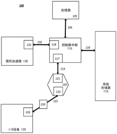
Semiconductor device based on UCIe interface
PatentActiveCN117222234A
Innovation
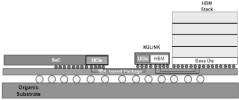
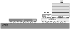
- Using semiconductor devices based on the UCIe interface, the SoC is decoupled from the HBM through joint dies, and the rewiring layer and organic substrate are used for interconnection, avoiding the silicon interposer, realizing the decoupling of the SoC and HBM memory, and through the on-chip bus Perform data exchange.
Supply Chain Implications for UCIe Implementation
The implementation of UCIe (Universal Chiplet Interconnect Express) technology introduces significant transformations across the semiconductor supply chain, requiring careful reconfiguration of existing manufacturing and assembly processes. Traditional monolithic chip production involves a single manufacturer controlling the entire process, whereas chiplet-based designs necessitate collaboration among multiple suppliers specializing in different components.
For UCIe implementation, supply chain complexity increases substantially as it requires coordination between foundries producing different chiplets, packaging facilities handling advanced integration, and testing services ensuring inter-chiplet communication reliability. This fragmentation creates new dependencies and potential bottlenecks that must be carefully managed to maintain production efficiency.
Yield management becomes particularly critical in the UCIe supply chain. While chiplet architectures theoretically improve overall yield by separating components, they simultaneously introduce new failure points at interconnect interfaces. Supply chain partners must develop shared quality metrics and testing protocols specifically designed for chiplet-to-chiplet connections to ensure consistent performance across different suppliers' components.
Inventory management strategies require significant adjustment when implementing UCIe technology. Companies must balance maintaining sufficient stocks of various chiplet types against the risk of obsolescence, particularly challenging given the rapid evolution of chiplet standards and specifications. This necessitates more sophisticated forecasting models that account for the interdependencies between different chiplet components.
Geographical distribution of the UCIe supply chain presents both opportunities and challenges. While distributed manufacturing can provide resilience against regional disruptions, it also increases logistics complexity and potential delays. Companies implementing UCIe technology must carefully evaluate the trade-offs between centralized and distributed production models based on their specific product requirements and market conditions.
Intellectual property management becomes more complex in a UCIe ecosystem, as multiple vendors must share interface specifications while protecting their proprietary technologies. This requires new contractual frameworks and collaboration models that balance openness at interfaces with protection of core intellectual assets, potentially reshaping traditional supplier relationships throughout the semiconductor industry.
Standardization Efforts and Industry Collaboration
The UCIe (Universal Chiplet Interconnect Express) standardization represents a pivotal collaborative effort in the semiconductor industry, bringing together major players to establish common protocols for chiplet-to-chiplet communication. This industry-wide initiative, launched in March 2022, includes founding members such as Intel, AMD, Arm, TSMC, Samsung, and Google, demonstrating unprecedented cooperation among traditionally competitive entities.
The standardization process for UCIe has been structured through a multi-tiered approach, with technical working groups focusing on physical layer specifications, protocol definitions, and testing methodologies. These collaborative efforts have accelerated the development of yield-cost sensitivity models that can be universally applied across different manufacturing processes and chiplet designs, creating a common framework for economic evaluation.
Industry collaboration extends beyond mere technical specifications to include shared testing methodologies and validation procedures. The UCIe Consortium has established specialized task forces dedicated to developing standardized yield metrics and cost modeling approaches, enabling more accurate comparisons between different implementation strategies. This collaborative approach has significantly reduced redundant research efforts across the industry.
The standardization efforts have also addressed the critical challenge of interoperability between chiplets from different vendors. By establishing common electrical and mechanical specifications, the industry has created an ecosystem where chiplets can be mixed and matched regardless of their origin, substantially improving manufacturing economics through increased volume and yield optimization across multiple applications.
Knowledge sharing within the consortium has been formalized through regular technical symposiums and publication of reference designs. These collaborative platforms have been instrumental in identifying common yield challenges and developing shared solutions, particularly for complex issues like die-to-die interface alignment and thermal management that significantly impact overall yield calculations in multi-chiplet packages.
The economic impact of these standardization efforts has been substantial, with early adopters reporting up to 30% reduction in integration costs when implementing UCIe-compliant designs. This cost reduction stems primarily from the ability to leverage standardized testing procedures, shared yield improvement techniques, and the emergence of specialized equipment optimized for UCIe manufacturing processes.
Looking forward, the UCIe Consortium has established a roadmap for continued collaboration, with planned extensions to the standard that will address emerging yield challenges in advanced packaging technologies. These future efforts will focus on developing more sophisticated yield-cost models that incorporate additional variables such as thermal performance, signal integrity at higher bandwidths, and reliability factors across diverse operating conditions.
Unlock deeper insights with Patsnap Eureka Quick Research — get a full tech report to explore trends and direct your research. Try now!
Generate Your Research Report Instantly with AI Agent
Supercharge your innovation with Patsnap Eureka AI Agent Platform!