UCIe Chiplet Interconnect EMI/EMC Compliance Toolkit
SEP 1, 20259 MIN READ
Generate Your Research Report Instantly with AI Agent
Patsnap Eureka helps you evaluate technical feasibility & market potential.
UCIe Chiplet Interconnect Background and Objectives
Universal Chiplet Interconnect Express (UCIe) represents a significant advancement in semiconductor integration technology, emerging as a response to the increasing challenges of traditional monolithic chip scaling. Developed through industry collaboration, UCIe aims to establish an open, standardized die-to-die interconnect framework that enables heterogeneous integration of chiplets from different vendors within a single package.
The evolution of UCIe technology can be traced back to the fundamental limitations of Moore's Law, which has traditionally guided semiconductor advancement. As process node scaling becomes increasingly difficult and expensive, the industry has pivoted toward chiplet-based designs that allow for more efficient manufacturing, improved yields, and greater design flexibility. This architectural shift began gaining momentum around 2017-2018, with early proprietary solutions from companies like Intel (EMIB), AMD (Infinity Fabric), and TSMC (CoWoS).
In March 2022, the UCIe consortium was formally established with founding members including Intel, AMD, Arm, ASE, Google, Meta, Microsoft, Qualcomm, Samsung, and TSMC. This marked a pivotal moment in the industry's move toward standardization of chiplet interfaces. The first UCIe 1.0 specification was released simultaneously, defining both the physical and protocol layers for die-to-die communication.
The primary technical objectives of UCIe include establishing high-bandwidth, low-latency connections between chiplets while maintaining energy efficiency. The standard aims to achieve data rates of up to 16 GT/s in its first generation, with a roadmap extending to 32 GT/s and beyond in future iterations. Power efficiency targets are set at less than 1 pJ/bit for advanced implementations.
A critical but often overlooked aspect of UCIe technology is electromagnetic interference and electromagnetic compatibility (EMI/EMC) compliance. As chiplet designs pack more high-speed interconnects into increasingly dense packages, managing electromagnetic emissions and ensuring signal integrity becomes paramount. The development of EMI/EMC compliance toolkits represents a crucial step toward enabling practical implementation of UCIe technology in commercial products.
The UCIe standard encompasses two primary packaging technologies: standard packages with organic substrates and advanced packaging using silicon interposers. This dual approach allows for flexibility in implementation while maintaining interoperability across different manufacturing processes and design methodologies.
Looking forward, the UCIe technology roadmap envisions progressive improvements in bandwidth density, power efficiency, and latency reduction. The standard is expected to evolve to support emerging computing paradigms such as artificial intelligence accelerators, high-performance computing, and edge computing applications, where heterogeneous integration offers significant advantages in performance and efficiency.
Market Demand Analysis for Chiplet Integration
The chiplet integration market is experiencing unprecedented growth as the semiconductor industry shifts from monolithic designs to disaggregated architectures. Current market analysis indicates that the global chiplet market is projected to grow at a compound annual growth rate of 40% through 2027, driven primarily by data center applications, high-performance computing, and artificial intelligence accelerators. This rapid expansion reflects the industry's recognition that traditional Moore's Law scaling alone cannot meet performance and cost requirements for next-generation computing systems.
Market research reveals that approximately 65% of semiconductor companies are actively investing in chiplet technology, with particular emphasis on standardized interconnect solutions. The Universal Chiplet Interconnect Express (UCIe) standard has emerged as a critical enabler for this market, with adoption rates increasing significantly since its introduction in 2022. Industry surveys indicate that over 80% of system architects consider electromagnetic interference and compatibility (EMI/EMC) compliance as a major concern when implementing chiplet-based designs.
The demand for UCIe Chiplet Interconnect EMI/EMC Compliance Toolkits stems from several market factors. First, as data rates exceed 16 GT/s in chiplet-to-chiplet communications, signal integrity and electromagnetic compatibility challenges increase exponentially. Second, regulatory requirements for electronic systems are becoming more stringent globally, with particular focus on high-frequency emissions from computing systems. Third, the cost of non-compliance and post-design remediation can exceed 30% of total development costs.
Market segmentation shows that hyperscalers and cloud service providers represent the largest potential customer base for EMI/EMC compliance tools, accounting for approximately 45% of the market. These organizations are implementing chiplet architectures to optimize performance per watt while maintaining flexibility in their hardware platforms. Telecommunications equipment manufacturers constitute the second-largest segment at 25%, followed by enterprise computing at 20%.
Regional analysis indicates North America leads in chiplet adoption and consequently in demand for compliance toolkits, representing approximately 40% of the global market. Asia-Pacific follows closely at 35%, with particularly strong growth in Taiwan, South Korea, and China where major semiconductor manufacturing is concentrated. Europe accounts for 20% of the market, with increasing interest driven by automotive and industrial applications where EMI/EMC requirements are especially stringent.
Customer interviews reveal that time-to-market pressure is intensifying the need for pre-validated compliance toolkits. Development teams report that EMI/EMC issues typically consume 15-20% of the design cycle when discovered late in the process. A comprehensive compliance toolkit could potentially reduce this to 5-7%, representing significant cost savings and competitive advantage.
Current EMI/EMC Challenges in Chiplet Interconnects
The integration of chiplets through UCIe (Universal Chiplet Interconnect Express) has introduced significant electromagnetic interference (EMI) and electromagnetic compatibility (EMC) challenges that were less prominent in traditional monolithic designs. As chiplet architectures become more prevalent, the density of high-speed interconnects has increased dramatically, creating new electromagnetic emission profiles that can affect both internal component functionality and compliance with regulatory standards.
Signal integrity issues represent one of the most pressing challenges in chiplet interconnects. The transition between dies introduces impedance discontinuities that can cause signal reflections, crosstalk, and ground bounce effects. These phenomena are particularly problematic at the high data rates (up to 32 GT/s) supported by UCIe, where even minor discontinuities can lead to significant signal degradation and increased electromagnetic emissions.
Power delivery network (PDN) noise has emerged as another critical concern. The distributed nature of chiplet designs creates complex power distribution paths with varying impedance characteristics. Simultaneous switching noise (SSN) generated across multiple chiplets can couple into sensitive analog circuits and radiate through package structures, compromising both performance and EMC compliance.
Inter-chiplet coupling mechanisms present unique challenges not seen in traditional designs. The close proximity of multiple dies with independent clock domains creates opportunities for mutual interference through substrate coupling, power/ground bounce, and near-field interactions. These coupling paths are difficult to model accurately during the design phase and can lead to unexpected EMI/EMC issues during product qualification.
Package resonance effects have become more pronounced with chiplet architectures. The physical dimensions and material properties of advanced packaging create resonant structures that can amplify electromagnetic emissions at specific frequencies. These resonances are particularly problematic when they coincide with clock harmonics or data rates used in the chiplet interconnects.
Current test methodologies are struggling to keep pace with these challenges. Traditional EMI/EMC testing approaches often fail to adequately characterize the complex emission patterns of chiplet-based systems. The industry lacks standardized test fixtures and procedures specifically designed for evaluating UCIe implementations, making compliance verification inconsistent across different testing facilities.
Simulation accuracy limitations further complicate the situation. Existing electromagnetic simulation tools often cannot efficiently model the multi-scale physics involved in chiplet designs, from on-die transistors to package-level effects. This modeling gap creates uncertainty in predicting EMI/EMC performance early in the design cycle, leading to costly redesigns when compliance issues are discovered during physical testing.
Current EMI/EMC Compliance Solutions
01 EMI/EMC shielding techniques for UCIe chiplet interconnects
Various shielding techniques are employed to ensure EMI/EMC compliance in UCIe chiplet interconnects. These include the use of conductive enclosures, ground planes, and specialized shielding materials that can absorb or reflect electromagnetic radiation. Advanced shielding designs incorporate multiple layers of different materials to address various frequency ranges of potential interference, ensuring that the chiplet interconnects maintain signal integrity while minimizing electromagnetic emissions.- EMI/EMC shielding techniques for UCIe chiplet interconnects: Various shielding techniques are employed to minimize electromagnetic interference (EMI) and ensure electromagnetic compatibility (EMC) in UCIe chiplet interconnects. These include the use of conductive enclosures, ground planes, and specialized shielding materials that can absorb or reflect electromagnetic radiation. Advanced shielding designs incorporate multiple layers of protection to prevent signal leakage and external interference, which is critical for maintaining signal integrity in high-speed chiplet-to-chiplet communications.
- Signal integrity and noise reduction in UCIe implementations: Maintaining signal integrity and reducing noise are essential for UCIe chiplet interconnect EMI/EMC compliance. This involves careful design of transmission lines, impedance matching, and implementation of noise cancellation techniques. Advanced signal conditioning circuits and equalization methods are used to compensate for channel losses and minimize crosstalk between adjacent channels. These approaches help ensure reliable data transmission across chiplet boundaries while minimizing electromagnetic emissions that could interfere with nearby components.
- Power distribution network design for EMI/EMC compliance: Effective power distribution network design is crucial for UCIe chiplet interconnect EMI/EMC compliance. This includes strategic placement of decoupling capacitors, careful routing of power planes, and implementation of power integrity solutions to minimize voltage fluctuations and current spikes. Advanced power delivery techniques incorporate low-inductance paths and controlled impedance structures to reduce electromagnetic emissions from power distribution networks, which can be significant sources of EMI in chiplet-based systems.
- Testing and verification methodologies for UCIe EMI/EMC compliance: Comprehensive testing and verification methodologies are essential to ensure UCIe chiplet interconnect EMI/EMC compliance. These include near-field and far-field emission measurements, susceptibility testing, and system-level EMI/EMC verification. Advanced simulation techniques are employed to predict potential EMI issues early in the design process, allowing for proactive mitigation strategies. Automated test equipment and specialized test fixtures are used to characterize the electromagnetic behavior of chiplet interconnects under various operating conditions.
- Packaging and integration solutions for EMI/EMC optimization: Advanced packaging and integration solutions play a critical role in optimizing EMI/EMC performance of UCIe chiplet interconnects. These include innovative substrate designs with embedded EMI suppression features, careful die placement strategies, and specialized interconnect structures that minimize radiation. 3D integration techniques and advanced materials are utilized to create compact chiplet packages with inherently better EMI/EMC characteristics. Thermal management solutions are also designed with EMI/EMC considerations to prevent thermal-induced electromagnetic issues.
02 Signal integrity and noise reduction in UCIe implementations
Maintaining signal integrity and reducing noise are critical aspects of UCIe chiplet interconnect EMI/EMC compliance. This involves implementing techniques such as differential signaling, controlled impedance routing, and proper termination strategies. Advanced signal conditioning circuits and equalization techniques are used to compensate for channel losses and minimize inter-symbol interference. These approaches help ensure reliable high-speed data transmission while keeping electromagnetic emissions within acceptable limits.Expand Specific Solutions03 Power distribution network design for EMI/EMC compliant chiplets
Effective power distribution network design is essential for UCIe chiplet interconnect EMI/EMC compliance. This includes implementing decoupling capacitor networks, power plane segmentation, and controlled power delivery impedance. Advanced power integrity solutions incorporate on-die and package-level voltage regulators with fast transient response to minimize switching noise. These techniques help maintain stable power delivery while reducing electromagnetic emissions from the power distribution network.Expand Specific Solutions04 Testing and verification methodologies for UCIe EMI/EMC compliance
Comprehensive testing and verification methodologies are implemented to ensure UCIe chiplet interconnects meet EMI/EMC compliance standards. These include near-field and far-field emission measurements, conducted emission testing, and immunity testing against external interference. Advanced simulation techniques are employed during the design phase to predict potential EMI/EMC issues before fabrication. Automated test equipment and specialized test fixtures are used to characterize the electromagnetic behavior of chiplet interconnects under various operating conditions.Expand Specific Solutions05 Packaging and integration strategies for EMI/EMC compliant UCIe designs
Innovative packaging and integration strategies play a crucial role in achieving EMI/EMC compliance for UCIe chiplet interconnects. These include the use of advanced substrate materials with controlled dielectric properties, embedded ground planes, and strategic via placement. Careful consideration is given to the physical layout and orientation of chiplets to minimize coupling paths for electromagnetic interference. Thermal management solutions are designed to not only address heat dissipation but also to minimize the impact on electromagnetic performance.Expand Specific Solutions
Key Industry Players in Chiplet Ecosystem
The UCIe Chiplet Interconnect EMI/EMC Compliance Toolkit market is in its early growth stage, characterized by increasing adoption of chiplet architectures in semiconductor design. The market is projected to expand significantly as chiplet technology becomes mainstream, driven by demands for higher performance and energy efficiency. Key players shaping the technological landscape include Intel, which leads development of the UCIe standard, alongside QUALCOMM, AMD (formerly ATI), and IBM, who are actively contributing to compliance solutions. Semiconductor manufacturers like GLOBALFOUNDRIES and Renesas are integrating these standards into their fabrication processes. The technology is approaching maturity with specialized testing companies such as SimYog Technology and Dongdian Testing providing dedicated EMI/EMC compliance solutions, while academic institutions like Beihang University contribute research advancements.
Intel Corp.
Technical Solution: Intel has developed a comprehensive UCIe Chiplet Interconnect EMI/EMC Compliance Toolkit that addresses electromagnetic interference and compatibility challenges in chiplet-based designs. Their solution incorporates advanced signal integrity analysis tools that can simulate and predict EMI/EMC issues at the die-to-die interface level. Intel's toolkit includes specialized test fixtures for physical validation of UCIe links, allowing designers to measure emissions and susceptibility across different operating conditions. The company has implemented adaptive equalization techniques that dynamically adjust signal characteristics to maintain compliance while optimizing performance. Intel's approach also features automated compliance testing software that can rapidly identify potential EMI/EMC violations before production, significantly reducing development cycles. Their toolkit supports both standard and advanced UCIe implementations, with particular emphasis on maintaining signal integrity at high data rates (up to 32 GT/s) while minimizing electromagnetic emissions.
Strengths: Intel's position as a founding member of the UCIe consortium gives them deep technical expertise and influence over standards development. Their toolkit benefits from extensive real-world validation across multiple product generations. Weaknesses: The solution may be optimized primarily for Intel's own chiplet ecosystem, potentially limiting compatibility with third-party components. Implementation requires significant engineering resources and specialized equipment.
QUALCOMM, Inc.
Technical Solution: Qualcomm has engineered a UCIe Chiplet Interconnect EMI/EMC Compliance Toolkit specifically optimized for mobile and power-constrained applications. Their solution features proprietary shielding techniques that minimize electromagnetic interference while maintaining the compact form factors required in mobile devices. Qualcomm's toolkit incorporates advanced power management capabilities that dynamically adjust signal characteristics based on transmission requirements, reducing EMI during low-bandwidth operations. The company has developed specialized test methodologies that can accurately characterize EMI/EMC performance under variable power conditions typical in mobile environments. Their approach includes sophisticated simulation models that account for the complex electromagnetic environments found in densely packed mobile devices, allowing designers to identify and mitigate potential issues early in the development process. Qualcomm's toolkit also features automated compliance verification tools that can rapidly assess UCIe implementations against both industry standards and mobile-specific requirements.
Strengths: Qualcomm's expertise in power-efficient design gives their toolkit particular advantages in battery-powered applications. Their solution is highly optimized for the space constraints of mobile devices. Weaknesses: The toolkit may prioritize power efficiency over maximum bandwidth in some scenarios. The specialized nature of their mobile-optimized approach might limit applicability in high-performance computing environments.
Critical Patents and Technical Literature Review
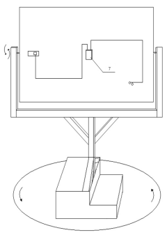
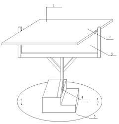
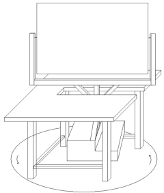
Testing device for electromagnetic compliance darkroom testing system
PatentInactiveCN202217021U
Innovation
- A test device for an electromagnetic compatibility darkroom test system is designed, including electromechanical components. The turntable and bracket controller are used to achieve precise position control and automatic rotation of the bracket table to ensure that the test environment remains unchanged. The turntable and bracket controller and gear system are used , the bracket panel and the rotating shaft are equipped with gears, and the three-dimensional rotation of the bracket panel is realized through electromechanical components and software control.

Technologies for a unified test and debug architecture
PatentWO2024205614A1
Innovation
- A unified test and debug architecture is implemented using an external hardware debug interface that is interface-agnostic, employing Universal Chiplet Interconnect Express (UCIe) packets for debug messages, allowing for seamless communication and interoperability between chiplets, and enabling testing at various stages from sort stage to infield debugging.

Standards and Certification Requirements
UCIe Chiplet Interconnect technology must adhere to rigorous standards and certification requirements to ensure interoperability, reliability, and compliance with electromagnetic interference (EMI) and electromagnetic compatibility (EMC) regulations. The Universal Chiplet Interconnect Express (UCIe) consortium has established comprehensive specifications that manufacturers must follow when implementing chiplet-based designs.
The primary regulatory frameworks governing UCIe implementations include FCC Part 15 (United States), CISPR 22/EN 55022 (Europe), and equivalent standards in other jurisdictions. These regulations establish limits for conducted and radiated emissions, ensuring that electronic devices do not interfere with other equipment. For UCIe specifically, compliance with these standards is critical due to the high-speed signaling (up to 16 GT/s in UCIe 1.0) that can potentially generate significant electromagnetic emissions.
The UCIe Compliance Program requires manufacturers to conduct extensive testing using specialized equipment and methodologies. This includes near-field and far-field emission measurements, susceptibility testing, and signal integrity verification. The EMI/EMC Compliance Toolkit provides standardized test procedures, reference designs, and validation methodologies to ensure consistent evaluation across different implementations.
Certification requirements for UCIe chiplet interconnects typically involve third-party laboratory testing and verification. The process includes pre-compliance testing during development, formal compliance testing prior to market release, and periodic re-certification when significant design changes occur. Documentation requirements are substantial, including detailed test reports, technical construction files, and declarations of conformity.
The UCIe consortium has also established specific performance thresholds for different application categories, recognizing that requirements may vary between consumer, industrial, automotive, and medical applications. For instance, automotive applications must meet the more stringent AEC-Q100 qualification requirements alongside basic EMI/EMC standards.
Manufacturers seeking UCIe certification must implement appropriate mitigation techniques to address potential EMI/EMC issues. These include proper shielding, controlled impedance routing, ground plane optimization, and strategic component placement. The Compliance Toolkit provides guidance on these mitigation strategies, along with reference designs that demonstrate successful implementation approaches.
As UCIe technology evolves, certification requirements are expected to become more stringent, particularly as data rates increase in future specifications. The consortium maintains a roadmap for updating standards and certification processes to address emerging challenges in high-speed chiplet interconnect technologies.
Thermal Management Considerations
Thermal management represents a critical consideration in the development and implementation of UCIe (Universal Chiplet Interconnect Express) technology. As chiplet-based designs continue to gain prominence in addressing the scaling challenges of traditional monolithic architectures, the thermal implications become increasingly significant. The high-density interconnects between chiplets generate substantial heat during operation, particularly at the interface boundaries where signal integrity must be maintained for reliable data transmission.
The thermal characteristics of UCIe implementations directly impact EMI/EMC compliance, as temperature fluctuations can alter electrical properties of materials and affect signal integrity. Higher operating temperatures typically increase electrical resistance in interconnect pathways, potentially leading to signal degradation and increased electromagnetic emissions. This thermal-electrical coupling effect necessitates comprehensive thermal management strategies as part of any EMI/EMC compliance toolkit.
Current thermal management approaches for UCIe implementations include advanced thermal interface materials (TIMs) specifically engineered for chiplet-to-chiplet and chiplet-to-package interfaces. These materials must balance thermal conductivity with electrical isolation properties to prevent thermal-induced EMI issues. Computational fluid dynamics (CFD) modeling has emerged as an essential tool in the pre-compliance phase, allowing designers to identify potential hotspots at interconnect junctions before physical prototyping.
The industry has observed that thermal gradients across chiplet interfaces can induce mechanical stress, potentially altering the electromagnetic characteristics of the interconnect. This phenomenon becomes particularly pronounced in heterogeneous integration scenarios where different materials with varying coefficients of thermal expansion are employed. The EMI/EMC compliance toolkit must therefore incorporate thermal cycling tests that evaluate interconnect performance across the expected operational temperature range.
Recent advancements in active cooling solutions specifically designed for chiplet architectures show promise in maintaining thermal stability. These include micro-fluidic cooling channels integrated directly into the interposer or package substrate, which can significantly reduce thermal resistance at critical interconnect points. Such innovations help maintain signal integrity under varying computational loads, thereby supporting consistent EMI/EMC performance.
For comprehensive compliance testing, thermal cameras and infrared microscopy have become essential components of the toolkit, enabling real-time monitoring of thermal distributions during electrical testing. This simultaneous thermal-electrical characterization allows for correlation between temperature variations and EMI/EMC anomalies, providing valuable insights for design optimization.
Unlock deeper insights with Patsnap Eureka Quick Research — get a full tech report to explore trends and direct your research. Try now!
Generate Your Research Report Instantly with AI Agent
Supercharge your innovation with Patsnap Eureka AI Agent Platform!