

UCIe Chiplet Interconnect Post-Silicon Validation Guide
SEP 1, 202510 MIN READ
Generate Your Research Report Instantly with AI Agent
PatSnap Eureka helps you evaluate technical feasibility & market potential.
UCIe Chiplet Technology Background and Objectives
Universal Chiplet Interconnect Express (UCIe) represents a significant advancement in semiconductor integration technology, emerging as a response to the increasing challenges of traditional monolithic chip scaling. The evolution of chiplet technology can be traced back to the early 2010s when semiconductor manufacturers began exploring disaggregated chip designs to overcome the limitations imposed by Moore's Law. UCIe, officially introduced in March 2022, stands as a collaborative industry effort to standardize die-to-die interconnects for chiplet-based designs.
The development of UCIe addresses the fundamental shift in semiconductor architecture from monolithic systems-on-chip (SoCs) to more modular, heterogeneous integration approaches. This transition has been driven by several factors, including the escalating costs of advanced process nodes, increasing design complexity, and the need for specialized silicon optimized for specific functions. By enabling the integration of multiple smaller dies (chiplets) manufactured using different process technologies, UCIe facilitates more cost-effective and flexible semiconductor solutions.
The technical evolution trajectory of chiplet interconnect technology has progressed from proprietary solutions like AMD's Infinity Fabric and Intel's EMIB (Embedded Multi-die Interconnect Bridge) toward open standards that promote interoperability. UCIe builds upon previous interconnect technologies while introducing standardized protocols for both die-to-die and package-to-package connections, supporting both standard and advanced packaging technologies.
The primary objective of UCIe is to establish an open, industry-standard interconnect that enables chiplets from different vendors to work seamlessly together. This interoperability aims to foster a more diverse and innovative chiplet ecosystem, allowing semiconductor companies to focus on their core competencies while leveraging complementary technologies from other providers. The standard encompasses both physical layer specifications and protocol stack definitions to ensure consistent performance and reliability across implementations.
Post-silicon validation represents a critical phase in the UCIe implementation lifecycle, focusing on verifying that manufactured chiplets conform to the standard's specifications and can interoperate as intended. This validation process aims to identify and resolve any issues related to signal integrity, power delivery, thermal management, and protocol compliance before chiplet-based products reach commercial deployment.
Looking forward, the UCIe technology roadmap anticipates increasing data rates, reduced power consumption, and enhanced security features to support next-generation computing requirements across data centers, high-performance computing, artificial intelligence, and edge computing applications. The standard is expected to evolve to accommodate emerging packaging technologies and address the growing demand for specialized computing architectures.
Market Demand Analysis for Chiplet-Based Solutions
The chiplet-based design approach has gained significant traction in the semiconductor industry, driven by several converging market factors. As traditional monolithic chip scaling faces increasing technical and economic challenges, the demand for modular, heterogeneous integration solutions has accelerated dramatically. Market research indicates that the global chiplet market is projected to grow at a compound annual growth rate exceeding 40% through 2027, reflecting the industry's rapid shift toward disaggregated architectures.
This market expansion is primarily fueled by data center and high-performance computing sectors, where the need for specialized processing capabilities combined with cost efficiency has become paramount. Cloud service providers and hyperscalers are increasingly adopting chiplet-based solutions to optimize performance-per-watt metrics while maintaining flexibility in their hardware infrastructure. The ability to mix and match different process nodes within a single package allows these companies to balance cutting-edge performance with economic sustainability.
Consumer electronics manufacturers represent another significant market segment embracing chiplet technology. As devices become more feature-rich while maintaining strict power and form factor constraints, the ability to integrate best-in-class components from different process technologies becomes increasingly valuable. This trend is particularly evident in premium smartphones, tablets, and emerging AR/VR devices where heterogeneous integration enables differentiated capabilities.
The automotive and industrial sectors are emerging as growth areas for chiplet adoption, particularly as these industries undergo digital transformation. Advanced driver assistance systems, autonomous vehicles, and industrial automation all require specialized processing capabilities that can benefit from the flexible integration approach that chiplets enable. These markets value the ability to combine mature, proven components with newer, specialized silicon.
From a supply chain perspective, the chiplet ecosystem is creating new business models and partnership opportunities. Fabless design companies can now focus on their core competencies while leveraging standardized interfaces like UCIe to integrate with complementary technologies. This has spurred the development of specialized chiplet providers and integration services, expanding the overall semiconductor value chain.
Geographically, North America and East Asia dominate the chiplet market, with major investments in both regions aimed at securing technological leadership in this strategic area. Government initiatives, particularly in the United States, Europe, and China, are providing additional market stimulus through funding programs specifically targeting advanced packaging and heterogeneous integration technologies.
The standardization of interfaces, particularly through initiatives like UCIe, is expected to accelerate market adoption by reducing integration risks and enabling broader ecosystem participation. As post-silicon validation methodologies mature, the market is likely to see increased confidence in chiplet-based designs, further driving adoption across industry segments.
UCIe Interconnect Technical Challenges and Status
UCIe (Universal Chiplet Interconnect Express) represents a significant advancement in chip-to-chip interconnect technology, enabling heterogeneous integration of chiplets within a package. However, the implementation and validation of UCIe interconnects present several technical challenges that must be addressed to ensure reliable operation and performance.
The primary challenge in UCIe interconnect technology lies in achieving high-speed signal integrity across the die-to-die interfaces. With data rates reaching up to 32 GT/s in UCIe 1.0 and potentially higher in future iterations, maintaining signal quality becomes increasingly difficult due to crosstalk, impedance mismatches, and power integrity issues. These challenges are exacerbated by the ultra-short channel characteristics of chiplet interconnects, which behave differently from traditional PCB-based interconnects.
Power management presents another significant hurdle, as the dense integration of chiplets creates thermal hotspots that can affect signal integrity and overall system reliability. The UCIe standard must accommodate various power states and transitions while maintaining consistent performance across different operational conditions.
Testing and validation methodologies for UCIe interconnects remain in nascent stages. Current post-silicon validation approaches must evolve to address the unique characteristics of die-to-die interfaces, including new test patterns, measurement techniques, and specialized equipment capable of probing these miniaturized connections.
Interoperability between chiplets from different vendors represents a fundamental challenge that UCIe aims to solve. However, ensuring seamless integration requires robust compliance testing and validation procedures that are still being developed by the industry consortium.
The current status of UCIe technology shows promising advancement. The UCIe 1.0 specification, released in March 2022, has established a foundation for standardized chiplet interconnects with three defined stack layers: physical layer, die-to-die adapter layer, and protocol layer. Major semiconductor companies including Intel, AMD, Arm, TSMC, and Samsung have joined the UCIe consortium, indicating strong industry support.
Initial implementations have demonstrated feasibility, with companies like Intel showcasing UCIe-based designs in their research papers and product roadmaps. However, widespread commercial deployment remains limited, with most applications still in research or early development phases.
Post-silicon validation tools and methodologies specific to UCIe are emerging but remain specialized. Equipment manufacturers are developing new capabilities for testing die-to-die interfaces at the required precision and speed, though comprehensive validation suites are still evolving.
The ecosystem around UCIe continues to develop, with EDA vendors incorporating UCIe-specific design and verification capabilities into their tools. However, a complete design-to-validation workflow optimized for UCIe implementations is still maturing.
Current Post-Silicon Validation Methodologies
01 Post-Silicon Validation Methodologies for UCIe Chiplet Interconnects
Various methodologies and techniques are employed for post-silicon validation of UCIe (Universal Chiplet Interconnect Express) chiplet interconnects. These include automated test pattern generation, boundary scan testing, and built-in self-test mechanisms specifically designed for chiplet-to-chiplet interfaces. These validation approaches help verify signal integrity, timing margins, and protocol compliance across die boundaries, ensuring reliable high-speed communication between chiplets in a package.- Post-silicon validation methodologies for UCIe chiplet interconnects: Various methodologies and techniques are employed for post-silicon validation of UCIe (Universal Chiplet Interconnect Express) chiplet interconnects. These include automated test pattern generation, boundary scan testing, and built-in self-test mechanisms specifically designed for chiplet-to-chiplet interfaces. These validation approaches help ensure signal integrity, timing margins, and protocol compliance across the high-speed interconnects between chiplets in advanced packaging configurations.
- Testing infrastructure for UCIe physical layer validation: Specialized testing infrastructure is developed for validating the physical layer of UCIe chiplet interconnects. This includes test fixtures, probe cards, and automated test equipment specifically designed to characterize high-speed die-to-die links. The physical layer validation focuses on parameters such as voltage margins, jitter tolerance, crosstalk, and other signal integrity aspects critical for reliable operation of chiplet interconnects at multi-gigabit speeds.
- Protocol and functional validation techniques for UCIe interfaces: Protocol and functional validation techniques ensure that UCIe chiplet interconnects operate according to specification at the transaction layer. These techniques include protocol checkers, compliance test suites, and functional coverage models that verify proper operation of the UCIe protocol stack. The validation process includes testing various protocol features such as flow control, error handling, power management, and interoperability between chiplets from different vendors.
- Performance characterization and optimization of UCIe interconnects: Methods for characterizing and optimizing the performance of UCIe chiplet interconnects focus on bandwidth, latency, and power efficiency metrics. These include stress testing under various operating conditions, thermal analysis, and power profiling. Advanced techniques such as statistical analysis and machine learning are employed to identify performance bottlenecks and optimize the interconnect for specific application requirements, ensuring that the chiplet-based system meets its performance targets.
- System-level validation of UCIe-based multi-chiplet designs: System-level validation approaches for UCIe-based multi-chiplet designs ensure proper integration and operation of the complete system. These include end-to-end functional testing, system boot validation, and application-level performance verification. The validation process addresses challenges such as clock domain crossing, power sequencing, and thermal management across multiple chiplets. Hardware-software co-validation techniques are also employed to ensure proper operation of the software stack on the chiplet-based hardware platform.
02 Testing Infrastructure for UCIe Interconnect Validation
Specialized testing infrastructure is developed for validating UCIe chiplet interconnects, including on-die test circuits, probe points, and debug interfaces. These testing structures enable comprehensive characterization of electrical parameters, power integrity, and thermal performance of the interconnect. The infrastructure supports both manufacturing tests and in-field diagnostics, allowing for detection of defects and performance degradation in chiplet-based systems.Expand Specific Solutions03 Signal Integrity and Performance Verification for UCIe Interfaces
Methods for verifying signal integrity and performance characteristics of UCIe interfaces focus on measuring and analyzing key parameters such as jitter, crosstalk, and eye diagrams. Advanced techniques including statistical analysis, machine learning-based pattern recognition, and adaptive equalization are employed to ensure reliable high-bandwidth communication between chiplets. These verification processes help optimize the interconnect design and validate compliance with UCIe specifications.Expand Specific Solutions04 System-Level Validation of UCIe-Based Multi-Chiplet Designs
System-level validation approaches for UCIe-based multi-chiplet designs involve end-to-end testing of functional paths across multiple chiplets. These methods include protocol-aware traffic generation, latency measurement, bandwidth testing, and power consumption analysis under various workloads. The validation ensures proper integration of chiplets from different vendors and verifies interoperability according to the UCIe standard, addressing challenges in heterogeneous integration.Expand Specific Solutions05 Automated Validation Frameworks for UCIe Chiplet Interconnects
Automated validation frameworks streamline the testing process for UCIe chiplet interconnects through test case generation, execution, and result analysis. These frameworks incorporate simulation-to-silicon correlation, regression testing capabilities, and comprehensive coverage metrics to ensure thorough validation. The automation enables efficient detection of corner cases, accelerates time-to-market, and supports continuous validation throughout the product lifecycle, addressing the complexity of modern chiplet-based system designs.Expand Specific Solutions
Key Industry Players in Chiplet Ecosystem
The UCIe Chiplet Interconnect market is currently in its early growth phase, characterized by rapid technological development and increasing industry adoption. The market size is projected to expand significantly as chiplet-based designs become more prevalent in addressing computing performance and power efficiency challenges. From a technical maturity perspective, industry leaders Intel, TSMC, and AMD are driving standardization efforts, while companies like Qualcomm, Samsung, and MediaTek are actively developing compatible solutions. GlobalFoundries and Jariet Technologies are focusing on specialized chiplet interconnect validation methodologies. The ecosystem is evolving with both established semiconductor giants and specialized firms contributing to validation frameworks, testing protocols, and post-silicon verification tools necessary for ensuring reliable chiplet-to-chiplet communication across heterogeneous integration platforms.
Intel Corp.
Technical Solution: Intel has pioneered the Universal Chiplet Interconnect Express (UCIe) standard and leads its development consortium. Their post-silicon validation approach for UCIe involves comprehensive testing methodologies including physical layer electrical validation, protocol layer compliance testing, and system-level interoperability verification. Intel's validation framework implements automated test suites that verify signal integrity across die-to-die interfaces, focusing on parameters such as eye diagrams, jitter measurements, and crosstalk analysis. Their methodology incorporates both in-die built-in self-test (BIST) circuits and external testing equipment to validate UCIe links at speeds up to 16 GT/s. Intel has developed specialized probe cards and test fixtures specifically designed for chiplet testing that enable high-precision measurements while maintaining signal fidelity across the interconnect.
Strengths: Industry-leading expertise as UCIe founder with comprehensive validation infrastructure and tools. Extensive experience with heterogeneous integration. Weaknesses: Proprietary aspects of their validation methodology may limit broader ecosystem adoption, and their solutions may be optimized primarily for their own manufacturing processes.
QUALCOMM, Inc.
Technical Solution: Qualcomm has developed a sophisticated UCIe post-silicon validation framework tailored for mobile and edge computing applications. Their approach emphasizes power efficiency validation alongside performance metrics, implementing specialized test vectors that stress the interconnect under various power states and thermal conditions. Qualcomm's validation methodology incorporates on-die measurement circuits that can characterize UCIe link performance in real-time during operation, allowing for dynamic adaptation and optimization. Their test infrastructure includes custom-designed automated test equipment (ATE) interfaces that can simultaneously validate multiple chiplet interconnects while simulating real-world application workloads. Qualcomm has particularly focused on validating the D2D (die-to-die) PHY layer reliability across process variations, implementing statistical analysis techniques to ensure robust operation across manufacturing tolerances.
Strengths: Advanced power-aware validation techniques optimized for mobile/edge applications with strong focus on energy efficiency metrics. Weaknesses: Validation approach may be overly specialized for mobile use cases, potentially limiting applicability to high-performance computing or data center environments.
Critical UCIe Validation Patents and Techniques
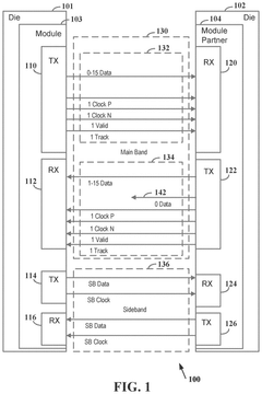
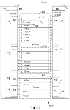
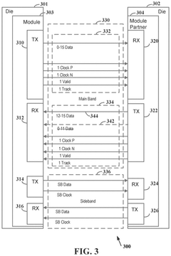
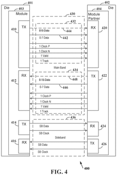
Variable link width in two directions for main band chip module connection
PatentPendingUS20240354279A1
Innovation
- Implementing a method to establish a die-to-die connection with a variable link width, allowing for independent configuration of transmit and receive data lanes through a sideband communication, enabling operation with different numbers of active data lanes in each direction to optimize power usage and data rates, and supporting fault tolerance by excluding faulty lines.
Mechanism To Improve The Reliability Of Sideband In Chiplets
PatentPendingUS20250086136A1
Innovation
- The method involves transitioning the UCIe link from an active state to a reset state and then initializing a different functional sideband, allowing for runtime configuration of sidebands and aggregation of multiple sidebands to enhance communication reliability and throughput.
Standardization Efforts and Industry Consortiums
The UCIe (Universal Chiplet Interconnect Express) ecosystem has witnessed significant collaborative efforts across the semiconductor industry to establish standardized frameworks for chiplet interconnection validation. The UCIe Consortium, formed in March 2022, represents the primary standardization body driving the development and adoption of the UCIe specification. This consortium brings together industry giants including Intel, AMD, Arm, TSMC, Samsung, and Qualcomm, creating a powerful alliance focused on establishing an open chiplet ecosystem.
The consortium's working groups have been instrumental in developing comprehensive validation methodologies that address the complex challenges of post-silicon validation for chiplet interconnects. These groups focus on various aspects including electrical specifications, protocol definitions, and compliance testing procedures, ensuring interoperability across different vendors' chiplets.
Beyond the UCIe Consortium, other industry organizations have contributed significantly to complementary standards that support the broader chiplet ecosystem. The JEDEC Solid State Technology Association has developed standards for memory interfaces that integrate with UCIe implementations. Similarly, the Open Compute Project (OCP) has established frameworks for server architectures that leverage chiplet-based designs, providing valuable validation contexts.
The Compute Express Link (CXL) Consortium has worked closely with UCIe stakeholders to ensure compatibility between these interconnect technologies, particularly important as both standards often coexist in modern system architectures. Their collaborative efforts have resulted in validation methodologies that address the interaction between UCIe and CXL interfaces.
Industry standardization has also extended to testing equipment and methodologies. The Automated Test Equipment (ATE) Consortium has developed specialized testing protocols for high-speed die-to-die interfaces, directly applicable to UCIe validation. These efforts have standardized test fixtures, signal integrity measurements, and performance benchmarking approaches.
Regional standardization bodies have also contributed to the UCIe validation ecosystem. The China Electronics Standardization Institute (CESI) and the European Telecommunications Standards Institute (ETSI) have developed region-specific validation guidelines that complement the core UCIe specification, addressing unique regulatory requirements while maintaining global interoperability.
These collaborative standardization efforts have been crucial in establishing a robust validation framework for UCIe implementations, enabling chiplet designers and system integrators to confidently develop interoperable components. The continued evolution of these standards will be essential as chiplet technology advances toward more complex integration scenarios and higher performance requirements.
Thermal Management Considerations for UCIe Implementation
Thermal management represents a critical challenge in the implementation of Universal Chiplet Interconnect Express (UCIe) technology. As chiplet-based designs increase in complexity and density, heat dissipation becomes a significant limiting factor affecting both performance and reliability. The UCIe standard, while providing high-bandwidth, low-latency interconnects between chiplets, introduces unique thermal considerations that must be addressed during post-silicon validation.
The primary thermal challenge in UCIe implementations stems from the concentrated power density at interconnect points. With die-to-die (D2D) interfaces operating at data rates up to 32 GT/s in advanced implementations, these junction points can become thermal hotspots. Post-silicon validation must therefore incorporate comprehensive thermal profiling across various workloads to identify potential thermal bottlenecks.
Effective thermal management strategies for UCIe implementations typically involve a multi-layered approach. At the package level, thermal interface materials (TIMs) with optimized thermal conductivity are essential for efficient heat transfer from chiplets to the heat spreader. The selection of appropriate TIMs must be validated through thermal resistance measurements during post-silicon testing, with particular attention to the thermal boundary resistance at chiplet interfaces.
Advanced cooling solutions, including integrated liquid cooling channels and vapor chambers, are increasingly being explored for high-performance UCIe implementations. Post-silicon validation protocols should include thermal cycling tests to evaluate the reliability of these cooling solutions under varying thermal loads and environmental conditions. Thermal imaging techniques, such as infrared microscopy, provide valuable data on temperature distribution across the chiplet assembly.
Dynamic thermal management (DTM) mechanisms represent another critical aspect of UCIe implementations. These include adaptive power management algorithms that modulate chiplet activity based on thermal feedback. Post-silicon validation must verify the responsiveness and effectiveness of these DTM systems, particularly during workload transitions that can cause rapid temperature fluctuations.
The physical layout of chiplets within a UCIe implementation significantly impacts thermal behavior. Validation engineers must evaluate different chiplet arrangements to optimize thermal spreading and minimize hotspots. Computational fluid dynamics (CFD) models, calibrated with post-silicon thermal measurements, can guide these optimization efforts and predict thermal performance under various operating conditions.
Long-term reliability testing constitutes an essential component of thermal validation for UCIe implementations. Accelerated aging tests under elevated temperatures help identify potential failure mechanisms related to thermal stress, including interconnect degradation and substrate warping. These tests inform lifetime reliability projections and help establish appropriate thermal design power (TDP) specifications for UCIe-based products.
Unlock deeper insights with PatSnap Eureka Quick Research — get a full tech report to explore trends and direct your research. Try now!
Generate Your Research Report Instantly with AI Agent
Supercharge your innovation with PatSnap Eureka AI Agent Platform!