

Test Access And DFT Methods In UCIe Chiplet Interconnect
SEP 1, 20259 MIN READ
Generate Your Research Report Instantly with AI Agent
PatSnap Eureka helps you evaluate technical feasibility & market potential.
UCIe Chiplet Interconnect Testing Background and Objectives
Universal Chiplet Interconnect Express (UCIe) has emerged as a transformative technology in the semiconductor industry, representing a paradigm shift from traditional monolithic chip designs to modular chiplet architectures. This evolution began in the mid-2010s as semiconductor manufacturers faced increasing challenges with Moore's Law, where the economic and technical feasibility of shrinking transistors became progressively more difficult. The chiplet approach allows different functional blocks to be manufactured using optimal process nodes and then integrated into a single package, offering significant advantages in cost, yield, and design flexibility.
The development of UCIe as an open industry standard was formally announced in March 2022, backed by major industry players including Intel, AMD, Arm, TSMC, and Samsung. This collaborative effort aimed to establish a unified interconnect standard that would enable chiplets from different vendors to communicate seamlessly within a package, fostering an open chiplet ecosystem. The standard defines both the physical layer and protocol stack for die-to-die interconnection, supporting data rates up to 32 GT/s in its first iteration.
Testing methodologies for chiplet-based designs represent a critical technical challenge that has evolved alongside the UCIe standard. Traditional Design for Test (DFT) approaches developed for monolithic chips are insufficient for the complex, multi-die architectures enabled by UCIe. The interconnect between chiplets introduces new failure modes and testing requirements that must be addressed to ensure reliable operation of integrated systems.
The primary technical objectives for UCIe testing include developing efficient test access mechanisms that can verify the integrity of die-to-die interconnects without excessive overhead. This involves creating standardized test interfaces that can operate across chiplets from different vendors while maintaining compatibility with existing test equipment and methodologies. Additionally, there is a need for test solutions that can be applied at multiple stages: at wafer level, after packaging, and in-system.
Current trends in UCIe testing are moving toward built-in self-test (BIST) capabilities that can validate interconnect functionality with minimal external equipment. There is also growing interest in adaptive test methodologies that can adjust testing parameters based on specific chiplet configurations and application requirements. The industry is working toward test standards that balance thoroughness with practical considerations of test time and cost.
The ultimate goal of UCIe testing development is to establish a robust, standardized testing framework that ensures reliable operation of heterogeneous chiplet-based systems while supporting the broader vision of an open chiplet ecosystem where components from multiple vendors can be seamlessly integrated.
Market Demand Analysis for Advanced Chiplet Testing Solutions
The global market for advanced chiplet testing solutions is experiencing robust growth, driven primarily by the accelerating adoption of chiplet-based architectures in semiconductor design. As traditional monolithic chip scaling faces increasing physical and economic limitations, the industry is rapidly pivoting toward disaggregated designs that leverage the Universal Chiplet Interconnect Express (UCIe) standard. Market research indicates that the chiplet market is projected to grow at a compound annual growth rate of over 40% through 2027, creating substantial demand for specialized testing methodologies.
The demand for UCIe-specific test access and Design for Testability (DFT) solutions is particularly acute in high-performance computing, data centers, and artificial intelligence applications. These sectors require increasingly complex systems-on-chip that benefit from the modularity and cost efficiency of chiplet designs. Industry surveys reveal that approximately 85% of semiconductor companies are actively exploring or implementing chiplet-based architectures, with testing solutions representing a critical enabler for widespread adoption.
A significant market driver is the economic advantage of chiplet designs. By enabling the integration of heterogeneous dies manufactured using different process nodes, chiplet architectures allow companies to optimize performance while controlling costs. However, this creates complex testing challenges at the interconnect level that conventional testing approaches cannot adequately address. The resulting gap has created a specialized market segment for UCIe-compliant testing solutions estimated to reach several hundred million dollars by 2025.
Regional analysis shows North America leading in demand for advanced chiplet testing solutions, followed by East Asia, particularly Taiwan, South Korea, and Japan. This geographic distribution aligns with the concentration of advanced semiconductor manufacturing and design capabilities. European markets are showing increased interest, particularly in automotive and industrial applications where reliability testing is paramount.
Customer segmentation reveals three primary market categories: integrated device manufacturers seeking comprehensive in-house testing capabilities, fabless semiconductor companies requiring specialized testing services, and third-party testing service providers expanding their offerings to include chiplet interconnect validation. Each segment presents distinct requirements and growth trajectories within the overall market.
The market is further characterized by strong demand for testing solutions that can address the unique challenges of UCIe implementations, including high-speed signal integrity verification, power delivery network validation, and thermal management assessment. Industry stakeholders consistently identify test coverage, throughput, and cost-effectiveness as the three most critical factors influencing purchasing decisions for chiplet testing solutions.
Current DFT Challenges in UCIe Chiplet Interconnects
The integration of chiplets through Universal Chiplet Interconnect Express (UCIe) presents significant challenges for Design for Testability (DFT) methodologies. As chiplet-based designs become more prevalent in addressing the limitations of monolithic integration, testing these complex multi-die systems has emerged as a critical bottleneck in the development pipeline.
One of the primary challenges is the limited test access to inter-chiplet connections. The high-density, fine-pitch interconnects in UCIe implementations often restrict traditional boundary scan testing approaches. With interconnect pitches reaching sub-10μm dimensions, physical probe access becomes nearly impossible, necessitating built-in test mechanisms that must be incorporated during the design phase.
Signal integrity issues compound the testing difficulties in UCIe environments. The high-speed nature of UCIe interfaces (up to 16 GT/s in UCIe 1.0) creates challenges for accurate at-speed testing. Conventional test methodologies struggle to detect subtle timing violations and signal degradation that may occur only under specific operating conditions or after prolonged use.
The heterogeneous integration aspect of chiplet designs introduces compatibility issues between different test methodologies. When chiplets from various vendors with diverse test infrastructures are combined, establishing a unified test strategy becomes exceedingly complex. The lack of standardized test interfaces across different chiplet implementations creates interoperability challenges that impede comprehensive system-level testing.
Power management during testing represents another significant hurdle. The power delivery network in multi-chiplet systems must be thoroughly tested, but traditional methods often fail to adequately stress these networks under realistic conditions. Additionally, thermal management during testing becomes critical as high-performance chiplets can generate substantial heat when operating at full test patterns.
Test data volume and bandwidth limitations present logistical challenges. Modern chiplet designs contain billions of transistors across multiple dies, generating enormous test data volumes that strain existing Automatic Test Equipment (ATE) capabilities. The limited number of test pins available for accessing internal chiplet structures further restricts test bandwidth.
Fault isolation in multi-chiplet systems presents unique diagnostic challenges. When a test fails, determining whether the fault resides in a specific chiplet, in the interconnect, or at the interface between chiplets requires sophisticated diagnostic capabilities that current tools may not fully support.
The industry also faces challenges in developing effective Known Good Die (KGD) testing methodologies for chiplets before integration. Without comprehensive pre-integration testing, defective chiplets may be incorporated into expensive packages, resulting in yield losses and increased manufacturing costs.
Mainstream DFT Methodologies for UCIe Implementation
01 UCIe Chiplet Interconnect Testing Architecture
The Universal Chiplet Interconnect Express (UCIe) architecture provides standardized methods for testing interconnects between chiplets. This includes built-in self-test (BIST) mechanisms specifically designed for die-to-die interfaces, boundary scan techniques, and test access ports that allow for comprehensive verification of chiplet interconnections. These testing architectures enable manufacturers to validate the integrity of high-speed connections between chiplets in multi-die packages.- UCIe Chiplet Interconnect Testing Architectures: Testing architectures specifically designed for UCIe (Universal Chiplet Interconnect Express) interfaces that enable comprehensive validation of chiplet-to-chiplet connections. These architectures incorporate specialized test access mechanisms to verify signal integrity, timing parameters, and protocol compliance across die boundaries. The testing frameworks typically include boundary scan cells, built-in self-test circuits, and loopback testing capabilities to ensure reliable operation of high-speed interconnects between chiplets.
- Design for Testability (DFT) Methods for Chiplet Interfaces: Design for Testability methods specifically tailored for chiplet-based systems using UCIe interfaces. These methods include test pattern generation techniques, scan chain implementations, and at-speed testing methodologies that address the unique challenges of testing disaggregated die architectures. The DFT approaches enable manufacturing defect detection, interconnect characterization, and performance validation while minimizing test time and maximizing fault coverage across chiplet boundaries.
- Built-In Self-Test (BIST) for UCIe Interfaces: Built-In Self-Test solutions specifically designed for UCIe interfaces that enable on-chip testing capabilities without requiring external test equipment. These BIST implementations include pattern generators, error detectors, and analysis circuits that can validate PHY layer functionality, link training sequences, and protocol compliance. The self-test mechanisms can operate during power-on, in-field operation, or manufacturing test to ensure reliable chiplet-to-chiplet communication.
- Test Access Mechanisms for Multi-Chiplet Packages: Test access mechanisms designed for multi-chiplet packages that utilize UCIe interconnects. These mechanisms include test wrappers, access ports, and control structures that enable efficient testing of complex chiplet-based systems. The test access solutions address challenges related to limited pin access, power constraints, and thermal considerations in densely packed chiplet assemblies while providing comprehensive test coverage for both intra-chiplet and inter-chiplet connections.
- Automated Test Equipment (ATE) Integration for UCIe Testing: Methods and systems for integrating Automated Test Equipment with UCIe-based chiplet designs to enable efficient production testing. These approaches include test protocol adaptations, specialized test fixtures, and software frameworks that allow standard ATE platforms to validate high-speed UCIe interfaces. The integration techniques address challenges related to high-frequency testing, signal integrity verification, and parallel testing of multiple chiplets to optimize manufacturing test costs and throughput.
02 Design for Testability (DFT) Methods for Chiplet Interfaces
Design for Testability methods specific to UCIe chiplet interfaces include scan chain implementations, loopback testing mechanisms, and specialized test pattern generators. These DFT approaches are integrated during the design phase to ensure testability of complex chiplet-based systems. The methods allow for fault detection, signal integrity verification, and parametric testing of die-to-die interfaces while minimizing test time and maximizing coverage of potential defects.Expand Specific Solutions03 At-Speed Testing for UCIe Interfaces
At-speed testing techniques for UCIe interfaces enable verification of chiplet interconnects at their operational frequencies. These methods include high-speed PRBS (Pseudo-Random Binary Sequence) testing, jitter tolerance testing, and eye diagram analysis. The techniques ensure that the chiplet interconnects meet performance requirements under actual operating conditions, validating bandwidth capabilities, latency characteristics, and signal integrity at full operational speeds.Expand Specific Solutions04 Automated Test Equipment (ATE) Integration for UCIe Testing
Integration of Automated Test Equipment with UCIe testing frameworks allows for efficient production testing of chiplet-based systems. This includes specialized test fixtures, probe card designs, and test program development methodologies specific to chiplet interconnects. The ATE integration enables high-volume manufacturing test of UCIe interfaces with optimized test flows, reducing test time while maintaining comprehensive coverage of potential interconnect defects.Expand Specific Solutions05 Known-Good-Die Testing for UCIe Chiplets
Known-Good-Die testing methodologies for UCIe chiplets ensure that individual dies are fully functional before integration into multi-chiplet packages. These approaches include wafer-level testing of UCIe interfaces, pre-bond testing techniques, and correlation methods between wafer-level and package-level test results. The methodologies help identify defective chiplets early in the manufacturing process, improving yield and reducing costs associated with packaging defective components.Expand Specific Solutions
Leading Companies in UCIe Test Technology Ecosystem
The UCIe chiplet interconnect test access and DFT methods market is currently in its growth phase, with increasing adoption of chiplet architectures driving demand for specialized testing solutions. The market is projected to expand significantly as heterogeneous integration becomes mainstream in semiconductor manufacturing. Intel leads the technological development with its foundational UCIe contributions, while Qualcomm, Huawei, and Samsung are actively developing compatible solutions. TSMC provides critical manufacturing support, and test equipment vendors like Advantest are creating specialized tools. Companies including AMD (formerly ATI/Xilinx) and IBM are contributing to standardization efforts, while specialized firms such as SiliConch Systems and Zhongke Ehiway are developing niche testing IP and methodologies.
Intel Corp.
Technical Solution: Intel has developed comprehensive test access methods for UCIe (Universal Chiplet Interconnect Express) chiplet interconnects, focusing on Design for Testability (DFT) solutions that enable efficient testing of multi-die packages. Their approach includes Built-In Self-Test (BIST) mechanisms specifically designed for die-to-die interfaces, allowing testing of PHY layer components without external test equipment. Intel's UCIe test architecture implements boundary scan techniques with specialized Test Access Points (TAPs) at the chiplet boundaries, facilitating interconnect testing between dies. They've also developed a hierarchical test methodology that enables both pre-packaging die-level testing and post-packaging system-level testing, with test patterns that can detect manufacturing defects in the die-to-die interfaces. Intel's solution incorporates IEEE 1149.1/JTAG compatibility for standardized test access, while adding UCIe-specific extensions to address the unique challenges of chiplet interconnects.
Strengths: Intel's solution leverages their extensive experience in chiplet technology and integration, providing comprehensive coverage for various fault models. Their hierarchical approach enables efficient testing at multiple stages of production. Weaknesses: The solution may require significant silicon area overhead for test structures and might introduce additional design complexity when implementing across heterogeneous chiplets from different vendors.
QUALCOMM, Inc.
Technical Solution: Qualcomm has developed a specialized DFT methodology for UCIe chiplet interconnects that focuses on high-speed SerDes testing and validation. Their approach implements a combination of loopback testing mechanisms and on-die measurement circuits to verify the integrity of die-to-die connections. Qualcomm's test solution incorporates dedicated Built-In Self-Test (BIST) engines that can generate pseudo-random bit sequences to stress-test the UCIe links at various operating conditions, measuring bit error rates and signal integrity parameters. They've implemented a modular test architecture that allows selective testing of individual lanes within the UCIe interface, enabling efficient fault isolation. Their DFT solution also includes specialized test modes that can characterize link performance across different voltage and frequency conditions, providing comprehensive coverage for manufacturing defects and parametric failures. Qualcomm's approach emphasizes minimizing test time while maintaining high fault coverage, with optimized test patterns that target specific failure mechanisms in chiplet interconnects.
Strengths: Qualcomm's solution excels in high-speed SerDes testing with sophisticated BIST capabilities that provide detailed performance metrics. Their modular approach allows for efficient fault isolation and diagnosis. Weaknesses: The solution may require significant computational resources for test pattern generation and analysis, potentially increasing test costs for complex multi-chiplet designs.
Key Test Access Patents and Technical Innovations
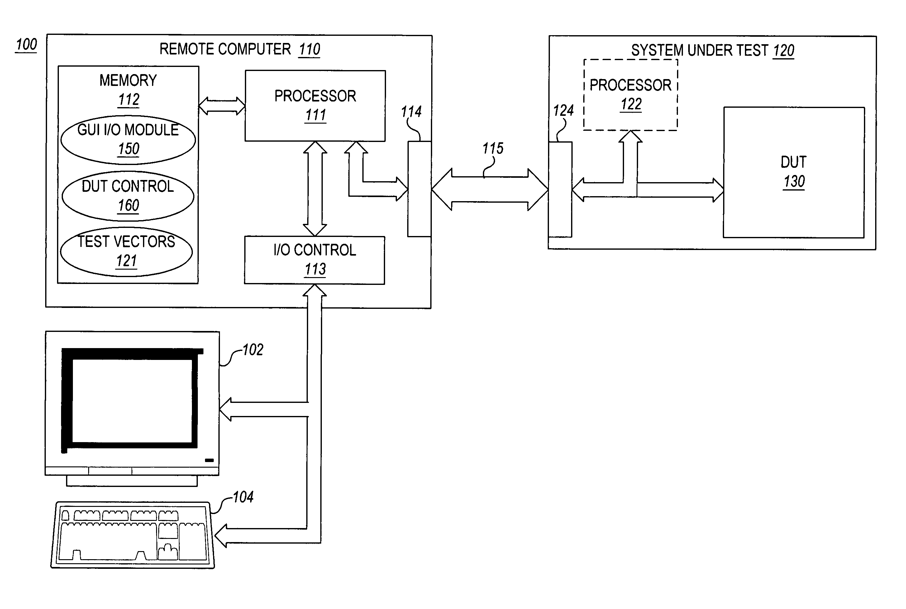
Remote integrated circuit testing method and apparatus
PatentActiveUS7237161B2
Innovation
- A method allowing remote testing and control of integrated circuits using a parallel cable and a graphical user interface, enabling test vectors to be applied and results to be analyzed without removing the IC from its native system, utilizing a Test Access Port (TAP) implementing the IEEE 1149.1 protocol.

Chiplet test circuit based on flexible configurable modules
PatentWO2023231276A1
Innovation
- Using a core chip test circuit based on a flexible configurable module (FCM), through a dual-channel obliquely symmetrical design structure and a control signal configuration module, the test configuration steps are simplified, and flexible control of the data transmission direction and multi-mode switching are achieved to meet the needs of horizontal dual lines transport and vertical bidirectional transport requirements, providing a common, scalable test access structure.


Standardization Efforts in Chiplet Testing
The standardization of chiplet testing methodologies has become increasingly critical as the semiconductor industry embraces disaggregated chip designs. Several industry consortia and standards bodies are actively working to establish unified frameworks for testing chiplet interconnects, with UCIe (Universal Chiplet Interconnect Express) being at the forefront of these efforts.
The UCIe Consortium, formed in 2022, has been developing comprehensive specifications that include dedicated sections on test methodologies for chiplet interconnects. Their working groups focus specifically on Design for Testability (DFT) requirements to ensure interoperability between chiplets from different vendors. The latest UCIe 1.1 specification includes enhanced provisions for test access mechanisms that address both pre-packaging and post-packaging testing scenarios.
JEDEC has also contributed significantly to chiplet testing standardization through its JC-13 committee, which has published guidelines for known good die testing applicable to chiplet architectures. These guidelines complement the UCIe specifications by providing detailed procedures for ensuring die quality before integration into multi-chiplet packages.
The IEEE has established the P2851 working group specifically focused on creating standards for inter-chiplet communication test methodologies. This group is developing test patterns and protocols that can verify the integrity of high-speed die-to-die interfaces like those used in UCIe implementations. Their work includes standardized Built-In Self-Test (BIST) architectures optimized for chiplet interconnects.
Open Compute Project (OCP) has launched initiatives to standardize chiplet testing within their Open Domain-Specific Architecture (ODSA) subproject. Their Chiplet Design Exchange (CDX) framework includes standardized test interfaces and methodologies that align with UCIe specifications while extending coverage to system-level testing considerations.
The CHIPS Alliance, another industry consortium, has been working on open-source DFT tools specifically designed for chiplet-based systems. Their efforts include developing standard test access port implementations and boundary scan methodologies compatible with UCIe interfaces.
Collaboration between these standardization bodies has accelerated in recent months, with joint working groups formed to ensure alignment between different standards. A notable development is the creation of the Chiplet Test Interoperability Framework (CTIF), which aims to harmonize test methodologies across different chiplet interface standards including UCIe, AIB, and BoW.
These standardization efforts collectively address critical challenges in chiplet testing, including test access mechanisms, fault models specific to die-to-die interfaces, and test pattern generation methodologies that can adequately verify the complex physical and protocol layers of modern chiplet interconnects.
Cost-Performance Tradeoffs in UCIe Test Strategies
When evaluating UCIe test strategies, organizations must carefully balance cost considerations against performance requirements. The implementation of comprehensive test access mechanisms in UCIe chiplet interconnects introduces significant cost factors that must be weighed against the benefits they provide. These costs manifest in multiple dimensions, including silicon area overhead, design complexity, and manufacturing expenses.
Silicon area dedicated to test infrastructure represents a direct cost impact, as test access ports (TAPs), boundary scan cells, and built-in self-test (BIST) circuits consume valuable die space that could otherwise be utilized for functional logic. This area overhead typically ranges from 2-5% of the total die area, depending on the comprehensiveness of the test infrastructure implemented. For high-volume production, this translates to measurable per-unit cost increases.
Design complexity introduces another cost dimension, as more sophisticated test methodologies require additional engineering resources during the design phase. The integration of advanced test features such as IEEE 1149.1/1500 compliance or UCIe-specific test structures necessitates specialized expertise and extends development timelines. Companies must evaluate whether these upfront investments will yield sufficient returns through improved test coverage and reduced test time.
Performance implications of test infrastructure must also be considered. While robust test mechanisms enhance long-term reliability, they may introduce parasitic capacitances and resistances that impact signal integrity across the UCIe interface. This is particularly critical for high-speed die-to-die connections operating at multi-gigabit rates, where even minor degradations in signal quality can affect overall system performance.
Test time represents another crucial trade-off factor. More comprehensive test methodologies generally require longer test cycles, directly impacting manufacturing throughput and cost. However, inadequate testing may result in field failures and warranty returns that ultimately prove more expensive. Finding the optimal balance requires careful modeling of defect rates, test coverage, and the cost implications of escaped defects.
The scalability of test strategies across different production volumes presents additional considerations. Highly automated test methodologies may require substantial upfront investment in equipment and infrastructure but can deliver significant cost advantages at high volumes. Conversely, more manual approaches may be economically viable for lower-volume, specialized applications despite higher per-unit test costs.
Unlock deeper insights with PatSnap Eureka Quick Research — get a full tech report to explore trends and direct your research. Try now!
Generate Your Research Report Instantly with AI Agent
Supercharge your innovation with PatSnap Eureka AI Agent Platform!