

Standards Roadmap And 2.0+ Updates For UCIe Chiplet Interconnect
SEP 1, 20259 MIN READ
Generate Your Research Report Instantly with AI Agent
PatSnap Eureka helps you evaluate technical feasibility & market potential.
UCIe Chiplet Interconnect Background and Objectives
Universal Chiplet Interconnect Express (UCIe) emerged as a critical technology in response to the semiconductor industry's growing challenges with traditional monolithic chip designs. As Moore's Law faces physical and economic limitations, the chiplet approach has gained prominence by disaggregating complex systems into smaller, specialized dies. UCIe was established in 2022 by an industry consortium including Intel, AMD, Arm, TSMC, Samsung, and other major players to create an open, standardized die-to-die interconnect technology.
The evolution of semiconductor technology has historically followed a trajectory of increasing integration and miniaturization. However, as process nodes shrink below 5nm, manufacturing costs and technical challenges have escalated dramatically. This has driven the industry toward chiplet-based designs, where multiple smaller dies are integrated into a single package. Prior to UCIe, various proprietary interconnect technologies existed, creating fragmentation in the ecosystem and limiting interoperability.
UCIe aims to establish a universal interconnect standard that enables chiplets from different vendors to work seamlessly together, fostering an open chiplet ecosystem. The standard encompasses both the physical layer specifications and protocols necessary for die-to-die communication within a package. The initial UCIe 1.0 specification focused on establishing the foundation for this ecosystem with standardized PHY, die-to-die adapters, and protocols.
The primary objectives of UCIe include enabling high-bandwidth, low-latency, and energy-efficient communication between chiplets while maintaining signal integrity. The standard seeks to support both standard and advanced packaging technologies, including silicon interposers and organic substrates. Additionally, UCIe aims to create a vibrant ecosystem where chiplets from different vendors can be mixed and matched, similar to how PCIe enabled interoperability between components at the board level.
The roadmap for UCIe 2.0+ updates represents the next evolution of this technology, addressing emerging requirements for higher bandwidth, improved power efficiency, and enhanced security features. These updates are critical as the industry moves toward more complex heterogeneous integration, incorporating diverse components such as CPUs, GPUs, memory, and specialized accelerators within a single package.
The technological trajectory of UCIe is closely aligned with broader industry trends, including the rise of AI/ML workloads, edge computing, and high-performance computing applications that demand unprecedented levels of computational density and efficiency. By establishing a common interconnect standard, UCIe aims to accelerate innovation while reducing development costs and time-to-market for advanced computing solutions.
Market Demand Analysis for Chiplet Technology
The chiplet technology market is experiencing unprecedented growth driven by the increasing demand for high-performance computing solutions across various industries. As traditional monolithic chip designs reach their physical and economic limits, chiplet-based architectures have emerged as a compelling alternative, offering improved performance, power efficiency, and cost-effectiveness. Market research indicates that the global chiplet market is projected to grow at a compound annual growth rate of over 40% from 2023 to 2030, reaching tens of billions of dollars by the end of the decade.
The primary market drivers for chiplet technology include the exponential growth in data center infrastructure, artificial intelligence applications, and high-performance computing systems. Cloud service providers are increasingly adopting chiplet-based solutions to address the computational demands of AI workloads, which require massive parallel processing capabilities and memory bandwidth. The rise of edge computing and IoT applications further amplifies the need for specialized, power-efficient computing solutions that chiplets can effectively deliver.
Consumer electronics manufacturers are also showing significant interest in chiplet technology as they seek to differentiate their products through enhanced performance while managing development costs. The automotive industry represents another substantial growth segment, with advanced driver-assistance systems and autonomous driving technologies requiring sophisticated computing platforms that can be efficiently implemented using chiplet architectures.
The UCIe (Universal Chiplet Interconnect Express) standard has emerged as a critical enabler for the chiplet ecosystem, addressing the interoperability challenges that previously limited widespread adoption. Market analysis shows that standardization efforts like UCIe are accelerating market growth by reducing integration risks and enabling a more diverse supplier ecosystem. The upcoming UCIe 2.0+ updates are anticipated to further expand market opportunities by enhancing interconnect capabilities and supporting more diverse integration scenarios.
From a geographical perspective, North America currently leads the chiplet market, driven by the presence of major semiconductor companies and hyperscale data center operators. However, Asia-Pacific is expected to witness the fastest growth, supported by substantial investments in semiconductor manufacturing infrastructure and government initiatives promoting technological self-sufficiency.
The market demand for chiplet technology is also influenced by broader industry trends, including the slowdown of Moore's Law, increasing chip design costs, and supply chain resilience concerns. Organizations are increasingly viewing chiplet-based designs as a strategic approach to mitigate these challenges while maintaining innovation momentum in semiconductor technology.
UCIe Technical Status and Implementation Challenges
UCIe (Universal Chiplet Interconnect Express) technology has evolved significantly since its introduction in 2022. Currently, the standard is at version 1.1, with the consortium actively working on version 2.0. The global adoption of UCIe has been uneven, with major semiconductor companies in North America and Asia leading implementation efforts. Companies like Intel, AMD, TSMC, and Samsung have made substantial investments in chiplet-based designs utilizing UCIe standards.
The primary technical challenges facing UCIe implementation revolve around several critical areas. First, achieving true interoperability between chiplets from different manufacturers remains difficult due to variations in implementation approaches and proprietary extensions. While the standard aims to create a universal interconnect, practical integration often requires extensive customization and testing.
Power efficiency presents another significant hurdle. As chiplet designs become more complex with higher data transfer rates, managing power consumption at the interconnect level becomes increasingly challenging. The current UCIe standard provides basic power management features, but optimizing power across heterogeneous chiplets requires sophisticated solutions not fully addressed in the current specification.
Signal integrity issues emerge as data rates increase, particularly in the physical layer implementation. Cross-talk, electromagnetic interference, and thermal effects can degrade signal quality, requiring advanced packaging technologies and careful design considerations. The industry is still developing best practices for maintaining signal integrity in high-density chiplet implementations.
Testing and validation methodologies for UCIe-based systems remain underdeveloped. Unlike traditional monolithic chips with established testing protocols, chiplet-based designs require new approaches to verify functionality across die boundaries. The lack of standardized testing frameworks increases development time and costs.
Geographically, UCIe technology development shows concentration in specific regions. North American companies like Intel and AMD have pioneered many aspects of the standard, while Asian manufacturers, particularly in Taiwan, South Korea, and increasingly China, focus on implementation and manufacturing optimization. European involvement has been more limited, primarily through research institutions and specialized semiconductor companies.
The ecosystem supporting UCIe is still maturing, with gaps in design tools, verification methodologies, and manufacturing processes. EDA vendors are working to incorporate chiplet-specific features into their tools, but comprehensive design flows optimized for UCIe remain a work in progress. This fragmented ecosystem creates additional barriers to widespread adoption, particularly for smaller companies with limited resources.
Current UCIe Implementation Solutions
01 UCIe architecture and implementation standards
The Universal Chiplet Interconnect Express (UCIe) architecture establishes standardized protocols for chiplet-to-chiplet communication within advanced packaging systems. These standards define physical layer specifications, protocol layers, and electrical parameters to ensure interoperability between chiplets from different manufacturers. The implementation standards include specifications for die-to-die interfaces, signal integrity requirements, and power delivery mechanisms that enable high-bandwidth, low-latency connections between integrated components.- UCIe standard development and evolution: The Universal Chiplet Interconnect Express (UCIe) standard has been evolving to address the growing needs of chiplet-based designs. The roadmap includes progressive improvements in data rates, power efficiency, and protocol support. The standard development focuses on establishing specifications for die-to-die interconnects that enable seamless integration of chiplets from different vendors, creating a more open ecosystem for heterogeneous integration.
- Physical layer implementations for chiplet interconnects: Physical layer implementations for UCIe focus on high-speed, low-power interconnects between chiplets. These implementations include advanced signaling techniques, equalization methods, and clock recovery mechanisms to ensure reliable data transmission across chiplet boundaries. The physical layer designs address challenges such as signal integrity, power consumption, and thermal management while supporting increasing bandwidth requirements for next-generation computing systems.
- Packaging technologies for chiplet integration: Advanced packaging technologies are crucial for implementing UCIe-based chiplet designs. These include silicon interposers, organic substrates, and advanced assembly techniques that enable high-density interconnects between chiplets. The packaging solutions address thermal management, mechanical stress, and electrical performance requirements while supporting the high bandwidth and low latency connections needed for chiplet-based systems.
- Protocol and interface standardization: The UCIe roadmap includes standardization of protocols and interfaces to ensure interoperability between chiplets from different vendors. This includes defining transaction protocols, flow control mechanisms, and error handling procedures. The standardization efforts aim to create a unified ecosystem where chiplets can be mixed and matched regardless of their manufacturer, enabling more flexible and cost-effective system designs.
- Testing and validation methodologies: Testing and validation methodologies for UCIe-compliant chiplets are essential for ensuring interoperability and reliability. These include standardized test procedures, compliance testing, and validation frameworks that verify proper implementation of the UCIe specifications. The roadmap includes development of test chips, reference designs, and validation tools that help manufacturers ensure their chiplets will work correctly when integrated with other UCIe-compliant components.
02 Advanced packaging technologies for UCIe integration
Advanced packaging technologies are critical for implementing UCIe standards in multi-chiplet designs. These include 2.5D and 3D integration methods, silicon interposers, and organic substrates that facilitate high-density interconnects between chiplets. The packaging approaches address thermal management challenges, mechanical stress considerations, and manufacturing yield optimization while maintaining the high-speed signaling capabilities required by UCIe specifications. These technologies enable heterogeneous integration of chiplets with different process nodes and functionalities.Expand Specific Solutions03 UCIe protocol enhancements and future roadmap
The UCIe standard continues to evolve with protocol enhancements that address emerging requirements for chiplet-based systems. Future roadmap developments include increased bandwidth capabilities, reduced power consumption, enhanced security features, and support for new use cases such as AI accelerators and specialized computing architectures. The roadmap also outlines compatibility with emerging memory interfaces, coherency protocols, and standardized testing methodologies to ensure long-term viability of the UCIe ecosystem across multiple technology generations.Expand Specific Solutions04 Testing and validation methodologies for UCIe compliance
Comprehensive testing and validation methodologies are essential for ensuring UCIe compliance across different chiplet implementations. These include standardized test patterns, signal integrity verification procedures, interoperability testing frameworks, and compliance certification processes. The methodologies address both pre-silicon validation through simulation and post-silicon testing using specialized equipment. They enable manufacturers to verify that their chiplet designs meet the electrical, timing, and protocol requirements specified in the UCIe standard, ensuring reliable operation in multi-vendor environments.Expand Specific Solutions05 System-level integration and optimization for UCIe-based designs
System-level integration considerations for UCIe-based designs encompass power management strategies, thermal solutions, and software optimization techniques. These include dynamic power scaling, chiplet-aware operating systems, and middleware that can efficiently utilize heterogeneous computing resources. The optimization approaches focus on balancing performance, power efficiency, and manufacturing cost while maintaining compliance with the UCIe standard. System architects must consider the entire stack from physical integration to application software to fully leverage the benefits of chiplet-based designs in various computing platforms.Expand Specific Solutions
Key Industry Players in Chiplet Ecosystem
The UCIe chiplet interconnect technology is currently in an early growth phase, with significant momentum building around standardization and 2.0+ updates. The market is expanding rapidly as chiplet-based designs become essential for advanced computing systems, driven by the need for heterogeneous integration and improved performance. Major semiconductor players including Intel, TSMC, Samsung, Qualcomm, and AMD (through ATI) are leading technical development, with Intel being a primary contributor to the UCIe standard. The technology is approaching early maturity with first-generation implementations, while 2.0+ updates aim to address higher bandwidth, reduced latency, and improved power efficiency. Chinese companies like Huawei and academic institutions such as the National University of Defense Technology are also actively participating, indicating the global strategic importance of this interconnect technology for future computing architectures.
Intel Corp.
Technical Solution: Intel is a founding member and key contributor to the UCIe (Universal Chiplet Interconnect Express) consortium. Their technical approach to UCIe focuses on an open die-to-die interconnect standard that enables chiplet-based designs across multiple process nodes and foundries. Intel's implementation leverages their EMIB (Embedded Multi-die Interconnect Bridge) and Foveros packaging technologies as complementary to UCIe. For UCIe 2.0+, Intel is driving advancements in physical layer specifications supporting higher bandwidth densities up to 32 GT/s per pin, improved power efficiency with new low-power states, and enhanced protocol layers for more efficient data movement between chiplets. Their solution includes standardized testing methodologies and compliance programs to ensure interoperability across the ecosystem. Intel has also developed reference designs and validation tools to accelerate adoption across the industry, positioning UCIe as the foundation for their disaggregated chip architecture strategy.
Strengths: Strong ecosystem influence as founding member; mature packaging technologies (EMIB/Foveros) that complement UCIe; extensive IP portfolio. Weaknesses: Potential competitive concerns from other foundries may limit full industry adoption; transitioning from proprietary interconnects to open standards requires significant investment and strategic shifts.
QUALCOMM, Inc.
Technical Solution: Qualcomm's approach to UCIe focuses on extending their mobile SoC expertise to a chiplet-based architecture. Their technical solution emphasizes power efficiency and high-bandwidth communication critical for mobile and edge computing applications. Qualcomm has developed specialized PHY layer implementations for UCIe that optimize for power-constrained environments, achieving up to 20% better energy efficiency compared to standard implementations. For UCIe 2.0+, Qualcomm is contributing advancements in cache coherency protocols and memory sharing mechanisms between heterogeneous chiplets, enabling more efficient processing for AI workloads at the edge. Their implementation includes custom controller logic that dynamically adjusts bandwidth and power states based on workload demands, maximizing battery life in mobile devices. Qualcomm is also developing security extensions for UCIe to enable trusted execution environments across chiplet boundaries, addressing a critical requirement for secure computing in distributed architectures.
Strengths: Industry-leading expertise in power-efficient designs; strong IP position in mobile connectivity that can extend to chiplet interconnects; vertical integration capabilities. Weaknesses: Less experience with data center scale implementations where other UCIe consortium members have stronger positions; potential challenges in adapting mobile-optimized approaches to broader computing markets.
Core UCIe 2.0+ Technical Innovations
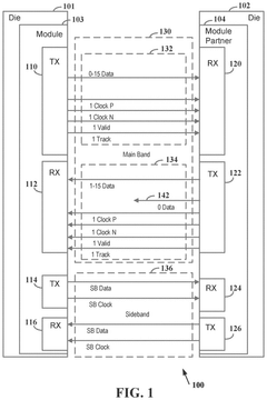
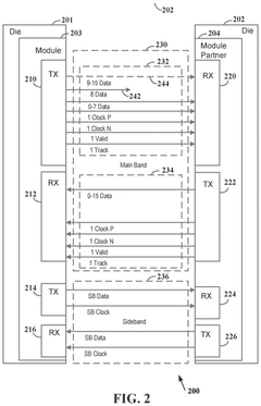
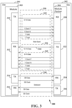
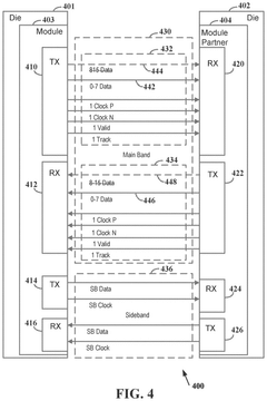
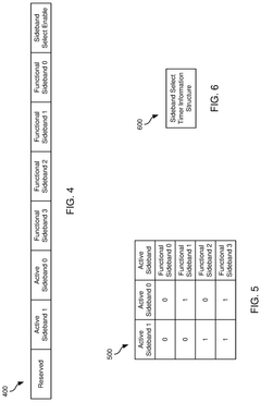
Variable link width in two directions for main band chip module connection
PatentPendingUS20240354279A1
Innovation
- Implementing a method to establish a die-to-die connection with a variable link width, allowing for independent configuration of transmit and receive data lanes through a sideband communication, enabling operation with different numbers of active data lanes in each direction to optimize power usage and data rates, and supporting fault tolerance by excluding faulty lines.
Mechanism To Improve The Reliability Of Sideband In Chiplets
PatentPendingUS20250086136A1
Innovation
- The method involves transitioning the UCIe link from an active state to a reset state and then initializing a different functional sideband, allowing for runtime configuration of sidebands and aggregation of multiple sidebands to enhance communication reliability and throughput.
Interoperability and Compatibility Considerations
Interoperability and compatibility represent critical dimensions for the UCIe (Universal Chiplet Interconnect Express) standard as it evolves toward version 2.0 and beyond. The heterogeneous integration of chiplets from different vendors necessitates robust frameworks ensuring seamless communication across diverse silicon components. Current UCIe 1.0 specifications establish baseline interoperability through standardized physical, protocol, and electrical layers, yet significant challenges remain as the ecosystem expands.
The UCIe Consortium has prioritized backward compatibility in its roadmap, ensuring that future implementations will maintain support for previous generation devices. This approach protects industry investments while enabling innovation. However, maintaining this compatibility while introducing performance enhancements presents technical challenges, particularly regarding signal integrity and power management across different process nodes.
Cross-vendor interoperability testing has emerged as a cornerstone activity within the UCIe ecosystem. The consortium has established working groups dedicated to developing comprehensive compliance test suites and certification programs. These initiatives aim to validate that chiplets from different manufacturers can effectively communicate when integrated on common substrates, with particular attention to latency, bandwidth, and error handling mechanisms.
Protocol translation layers represent another critical consideration in the UCIe roadmap. As the standard evolves to accommodate diverse interface requirements from memory, I/O, and accelerator chiplets, efficient protocol bridges must be developed. The 2.0+ specifications are expected to introduce enhanced protocol abstraction layers that simplify integration while maintaining performance targets.
Security and trust boundaries between chiplets from different vendors introduce additional interoperability challenges. The UCIe roadmap addresses these concerns through standardized authentication mechanisms and secure communication channels between chiplets. These features are particularly important for applications in financial services, healthcare, and government sectors where data protection requirements are stringent.
Power management compatibility across chiplets represents another focus area for UCIe 2.0+. The standard is evolving to include more sophisticated power state coordination mechanisms, allowing heterogeneous chiplets to efficiently manage thermal constraints while optimizing system-level energy consumption. This capability becomes increasingly important as chiplet-based designs scale to more complex configurations.
Looking forward, the UCIe Consortium is developing enhanced interoperability frameworks for specialized domains such as AI accelerators, where custom data formats and computational patterns require standardized interfaces. These domain-specific extensions will maintain core compatibility while enabling optimized performance for targeted workloads, representing a balanced approach to ecosystem expansion.
Industry Adoption Barriers and Strategies
Despite the promising technical foundation of UCIe (Universal Chiplet Interconnect Express), several significant barriers impede its widespread industry adoption. The heterogeneous integration ecosystem faces standardization challenges as companies with established proprietary interconnect technologies may resist transitioning to UCIe due to substantial investments in their existing solutions. This resistance creates market fragmentation that slows universal adoption across the semiconductor industry.
Technical implementation barriers present another major challenge. The complexity of implementing UCIe across different manufacturing processes and technology nodes requires substantial engineering resources and expertise. Many smaller companies lack the technical capabilities and financial resources to integrate UCIe into their design workflows, creating an adoption gap between industry leaders and smaller players.
Intellectual property concerns further complicate adoption. While UCIe is positioned as an open standard, questions regarding licensing terms, patent pools, and royalty structures remain partially unresolved. Companies hesitate to commit without clear understanding of long-term IP implications and potential costs associated with implementation.
Supply chain readiness represents another critical barrier. The ecosystem of testing equipment, verification tools, and manufacturing processes specifically optimized for UCIe-based chiplet designs remains underdeveloped. This infrastructure gap increases implementation risks and costs for early adopters.
To overcome these barriers, several strategic approaches are emerging. Industry consortiums and working groups are developing comprehensive implementation guidelines, reference designs, and validation methodologies to reduce technical uncertainty. These collaborative efforts aim to create a shared knowledge base that lowers the entry barrier for new adopters.
Financial incentives through government programs and industry partnerships are being established to offset initial implementation costs, particularly for smaller companies and academic institutions. These initiatives help distribute the financial burden of adoption across the ecosystem rather than placing it solely on individual companies.
Open-source development frameworks for UCIe implementation are gaining traction, providing accessible design tools and verification environments that reduce development costs. These frameworks democratize access to chiplet technology across a broader range of organizations.
Phased adoption strategies allow companies to gradually integrate UCIe alongside existing interconnect technologies, creating migration paths that preserve investments while enabling transition to the new standard. This approach reduces disruption while still moving the industry toward greater standardization.
Unlock deeper insights with PatSnap Eureka Quick Research — get a full tech report to explore trends and direct your research. Try now!
Generate Your Research Report Instantly with AI Agent
Supercharge your innovation with PatSnap Eureka AI Agent Platform!