UCIe Chiplet Interconnect Bump Pitch And Yield Tradeoffs Analysis
SEP 1, 20259 MIN READ
Generate Your Research Report Instantly with AI Agent
Patsnap Eureka helps you evaluate technical feasibility & market potential.
UCIe Chiplet Interconnect Evolution and Objectives
Universal Chiplet Interconnect Express (UCIe) represents a significant advancement in semiconductor integration technology, emerging as a response to the increasing challenges of traditional monolithic chip scaling. The evolution of UCIe technology can be traced back to the fundamental limitations encountered in Moore's Law progression, where physical constraints and economic factors began to impede the traditional approach of packing more transistors onto a single silicon die.
The development of chiplet technology marks a paradigm shift in semiconductor design philosophy, moving from monolithic integration to a more modular approach. This evolution began with early multi-chip module (MCM) technologies in the 1990s, progressed through 2.5D and 3D integration in the 2000s, and has now culminated in the standardized chiplet interconnect frameworks we see today with UCIe.
UCIe specifically addresses the critical need for a standardized interconnect protocol that enables heterogeneous integration of chiplets from different vendors and manufacturing processes. The first UCIe 1.0 specification was released in March 2022, establishing a foundation for die-to-die interconnect that spans multiple packaging technologies including both standard and advanced packaging options.
The primary objective of UCIe technology is to enable a disaggregated approach to system design, where specialized functional blocks can be manufactured using optimal process nodes and then integrated into a cohesive system. This approach aims to overcome the yield, cost, and performance limitations associated with large monolithic dies while maintaining the benefits of tight integration.
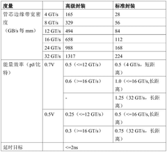
A key technical goal of UCIe is to provide high-bandwidth, low-latency, and energy-efficient communication between chiplets. The specification targets data rates ranging from 16 GT/s to 32 GT/s per pin in its initial implementations, with a roadmap for higher speeds in future iterations. This performance is critical for applications in high-performance computing, artificial intelligence, and data centers where data movement between processing elements is often a bottleneck.
Another crucial objective is establishing an ecosystem that promotes interoperability and standardization across the semiconductor industry. By creating an open standard, UCIe aims to foster innovation while reducing development costs and time-to-market for complex semiconductor products. This ecosystem approach is supported by a consortium of major industry players including Intel, AMD, Arm, TSMC, Samsung, and others.
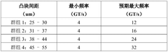
The evolution of UCIe is closely tied to advancements in bump pitch technology, as the density and reliability of interconnects directly impact the overall performance and yield of chiplet-based systems. As bump pitch continues to decrease from current standards (typically 40-55μm) toward finer pitches (potentially sub-30μm), the tradeoffs between interconnect density, manufacturing yield, and system cost become increasingly critical considerations in the UCIe technology roadmap.
The development of chiplet technology marks a paradigm shift in semiconductor design philosophy, moving from monolithic integration to a more modular approach. This evolution began with early multi-chip module (MCM) technologies in the 1990s, progressed through 2.5D and 3D integration in the 2000s, and has now culminated in the standardized chiplet interconnect frameworks we see today with UCIe.
UCIe specifically addresses the critical need for a standardized interconnect protocol that enables heterogeneous integration of chiplets from different vendors and manufacturing processes. The first UCIe 1.0 specification was released in March 2022, establishing a foundation for die-to-die interconnect that spans multiple packaging technologies including both standard and advanced packaging options.
The primary objective of UCIe technology is to enable a disaggregated approach to system design, where specialized functional blocks can be manufactured using optimal process nodes and then integrated into a cohesive system. This approach aims to overcome the yield, cost, and performance limitations associated with large monolithic dies while maintaining the benefits of tight integration.
A key technical goal of UCIe is to provide high-bandwidth, low-latency, and energy-efficient communication between chiplets. The specification targets data rates ranging from 16 GT/s to 32 GT/s per pin in its initial implementations, with a roadmap for higher speeds in future iterations. This performance is critical for applications in high-performance computing, artificial intelligence, and data centers where data movement between processing elements is often a bottleneck.
Another crucial objective is establishing an ecosystem that promotes interoperability and standardization across the semiconductor industry. By creating an open standard, UCIe aims to foster innovation while reducing development costs and time-to-market for complex semiconductor products. This ecosystem approach is supported by a consortium of major industry players including Intel, AMD, Arm, TSMC, Samsung, and others.
The evolution of UCIe is closely tied to advancements in bump pitch technology, as the density and reliability of interconnects directly impact the overall performance and yield of chiplet-based systems. As bump pitch continues to decrease from current standards (typically 40-55μm) toward finer pitches (potentially sub-30μm), the tradeoffs between interconnect density, manufacturing yield, and system cost become increasingly critical considerations in the UCIe technology roadmap.
Market Demand for Advanced Chiplet Integration
The demand for advanced chiplet integration technologies has experienced exponential growth in recent years, driven primarily by the semiconductor industry's need to overcome the limitations of traditional monolithic chip designs. As Moore's Law faces increasing physical and economic constraints, chiplet-based architectures have emerged as a viable alternative for continuing performance scaling while managing costs and manufacturing complexity.
Market research indicates that the global chiplet market is projected to grow at a CAGR of 40% from 2023 to 2030, with the total addressable market expected to reach $50 billion by 2030. This growth is fueled by increasing adoption across multiple sectors including high-performance computing, data centers, artificial intelligence accelerators, and telecommunications infrastructure.
The UCIe (Universal Chiplet Interconnect Express) standard has become a critical enabler for this market expansion. Industry surveys show that 85% of semiconductor companies are either implementing or evaluating UCIe for future product designs. The standard's promise of interoperability between chiplets from different vendors has created new market opportunities and business models centered around specialized chiplet development.
Data center operators represent the largest current market segment, with their demand driven by the need for customized compute solutions that balance performance, power efficiency, and cost. Cloud service providers are particularly interested in UCIe-based solutions that allow for rapid deployment of specialized AI and machine learning hardware configurations.
Consumer electronics manufacturers are increasingly exploring chiplet-based designs for next-generation mobile devices, AR/VR equipment, and edge computing products. Market analysis shows that these companies value the ability to integrate best-in-class components while maintaining competitive form factors and power profiles.
The automotive sector represents an emerging but rapidly growing market for advanced chiplet integration. As vehicles incorporate more sophisticated driver assistance systems and autonomous capabilities, the demand for high-performance, reliable computing platforms has intensified. UCIe's standardized approach offers automotive manufacturers a path to scalable solutions that can meet stringent reliability requirements.
Market surveys indicate that customers across all segments are particularly focused on the yield-cost tradeoffs in chiplet integration. As bump pitch decreases to enable higher bandwidth density, the associated yield challenges directly impact product costs and time-to-market. Industry analysts report that a 10% improvement in yield at advanced bump pitches could translate to approximately 15-20% cost reduction in final assembled products, representing a significant competitive advantage.
Current Challenges in Bump Pitch Scaling
As the semiconductor industry continues to advance, the scaling of bump pitch in UCIe (Universal Chiplet Interconnect Express) chiplet interconnects faces significant technical challenges. Current state-of-the-art bump pitch in high-volume manufacturing ranges between 30-40μm, with research demonstrations pushing boundaries to 20μm and below. However, this aggressive scaling trajectory encounters multiple barriers that impact manufacturing yield and reliability.
The primary challenge lies in the fundamental trade-off between bump pitch reduction and manufacturing yield. As bump pitch decreases, the process window for successful interconnect formation narrows substantially. Statistical analysis shows that yield degradation follows an exponential rather than linear relationship with pitch reduction, creating a critical inflection point where further miniaturization becomes economically unfeasible.
Material limitations present another significant obstacle. Traditional solder-based interconnects experience increasing electromigration and thermomechanical stress issues at finer pitches. The surface tension effects of molten solder become more pronounced at sub-30μm dimensions, leading to bridging defects and non-uniform bump formation. Alternative materials such as copper pillars with solder caps offer improved performance but introduce new process integration challenges.
Alignment precision requirements escalate dramatically with decreasing bump pitch. Current lithography and placement tools struggle to maintain the necessary accuracy at pitches below 25μm. The required alignment precision follows a quadratic relationship with bump pitch reduction, necessitating substantial equipment upgrades that impact manufacturing economics.
Inspection and quality control methodologies face resolution limitations when examining ultra-fine pitch interconnects. Conventional optical inspection techniques become inadequate, forcing a transition to more expensive and time-consuming electron microscopy methods. This creates bottlenecks in high-volume manufacturing environments and increases production costs.
Thermal management becomes increasingly problematic as bump density increases. The reduced cross-sectional area of finer-pitch bumps limits heat dissipation capabilities, potentially leading to localized hotspots and reliability concerns. Thermal modeling indicates that cooling solutions must evolve significantly to accommodate the higher power densities associated with advanced chiplet architectures.
Underfill processes, critical for mechanical stability and reliability, encounter significant challenges with decreasing bump pitch. Capillary flow dynamics become less predictable at sub-30μm spacings, leading to void formation and incomplete coverage. This necessitates the development of new underfill materials and application techniques specifically optimized for fine-pitch applications.
Existing Bump Pitch Solutions and Yield Management Approaches
01 UCIe bump pitch optimization for chiplet interconnects
The Universal Chiplet Interconnect Express (UCIe) standard defines specific bump pitch requirements for chiplet interconnects. Optimizing the bump pitch is crucial for achieving high-density connections between chiplets while maintaining signal integrity. Finer bump pitches allow for more interconnects in a given area, enabling higher bandwidth between chiplets. However, as bump pitch decreases, manufacturing challenges increase, requiring advanced lithography and alignment techniques to maintain yield.- UCIe bump pitch optimization for chiplet interconnects: The Universal Chiplet Interconnect Express (UCIe) standard defines specific bump pitch requirements for chiplet interconnects. Optimizing the bump pitch is crucial for achieving high-density interconnections between chiplets while maintaining signal integrity. Smaller bump pitches allow for more connections in a given area, enabling higher bandwidth between chiplets. However, the pitch must be carefully balanced with manufacturing capabilities to ensure reliable connections.
- Yield improvement techniques for UCIe chiplet manufacturing: Various techniques are employed to improve manufacturing yield in UCIe chiplet interconnects. These include advanced inspection methods, redundant bump designs, and self-healing interconnect technologies. Process optimization strategies focus on controlling bump height uniformity and coplanarity. Additionally, thermal cycling tests and reliability modeling help identify potential failure modes early in the manufacturing process, leading to improved overall yield rates for chiplet-based systems.
- Advanced materials for UCIe bump interconnects: Novel materials are being developed to enhance the performance and reliability of UCIe chiplet interconnects. These materials offer improved electrical conductivity, thermal stability, and mechanical strength compared to traditional solder bumps. Some approaches incorporate composite materials that can withstand the thermal and mechanical stresses encountered during operation. The selection of appropriate bump materials is critical for achieving the fine pitch requirements of UCIe while maintaining high yield and reliability.
- Testing and quality control for UCIe interconnects: Specialized testing methodologies have been developed to ensure the quality and reliability of UCIe chiplet interconnects. These include electrical testing for connectivity, resistance measurements, and high-frequency signal integrity verification. Advanced imaging techniques such as X-ray inspection and acoustic microscopy help detect defects in the bump connections. Automated test equipment specifically designed for chiplet testing enables high-throughput screening, which is essential for maintaining yield rates in volume production.
- Integration of UCIe with advanced packaging technologies: UCIe chiplet interconnect technology is being integrated with various advanced packaging approaches to optimize system performance. These include 2.5D and 3D integration schemes, silicon interposers, and embedded bridge technologies. The combination of UCIe with these packaging technologies enables heterogeneous integration of chiplets from different process nodes and manufacturers. Careful consideration of thermal management and mechanical stress is required when designing these integrated systems to maintain high yield and reliability.
02 Yield improvement techniques for UCIe chiplet interconnects
Various techniques are employed to improve the yield of UCIe chiplet interconnects. These include redundant bump structures, self-alignment mechanisms, and improved underfill materials. Advanced inspection and testing methodologies help identify defects early in the manufacturing process. Additionally, thermal management solutions are implemented to prevent bump failures due to thermal stress during operation. These yield improvement techniques are essential for the commercial viability of chiplet-based designs using the UCIe standard.Expand Specific Solutions03 Advanced materials for UCIe bump connections
The selection of materials for UCIe bump connections significantly impacts both performance and yield. Advanced solder compositions with improved mechanical properties help withstand thermal cycling and mechanical stress. Novel underfill materials provide better protection against environmental factors while maintaining electrical performance. Barrier metals and under-bump metallization layers are optimized to prevent intermetallic compound formation that could compromise connection reliability. These material innovations enable finer pitch interconnects while maintaining acceptable yield rates.Expand Specific Solutions04 Manufacturing processes for high-density UCIe interconnects
Specialized manufacturing processes are developed to achieve the high-density interconnects required by the UCIe standard. These include advanced lithography techniques for precise bump formation, improved alignment methods for accurate die placement, and optimized reflow processes to ensure proper bump formation. Innovations in pick-and-place equipment enable the handling of thin chiplets with minimal damage. Process control monitoring systems help maintain consistency across high-volume manufacturing, which is essential for achieving acceptable yield rates with fine-pitch UCIe interconnects.Expand Specific Solutions05 Testing and reliability assessment of UCIe chiplet interconnects
Comprehensive testing and reliability assessment methodologies are crucial for UCIe chiplet interconnects. These include electrical testing for connectivity, high-frequency signal integrity testing, and thermal cycling tests to evaluate long-term reliability. Non-destructive inspection techniques such as X-ray and acoustic microscopy help identify hidden defects in bump connections. Accelerated life testing protocols are developed specifically for chiplet interconnects to predict field reliability. These testing approaches help identify yield-limiting factors and guide process improvements for UCIe interconnect manufacturing.Expand Specific Solutions
Key Industry Players in Chiplet Ecosystem
The UCIe chiplet interconnect technology is currently in an early growth phase, with market expansion driven by increasing demand for heterogeneous integration in high-performance computing. The market is projected to grow significantly as chiplet-based designs become more prevalent in data centers and AI applications. Technologically, the industry faces critical tradeoffs between bump pitch reduction and manufacturing yield, with leading players developing different approaches. Intel and TSMC are pioneering advanced packaging technologies, while Qualcomm, AMD (formerly Xilinx), and Samsung are actively developing UCIe-compatible solutions. IBM and NXP are contributing to standardization efforts, with specialized players like STATS ChipPAC and Jariet Technologies focusing on specific interconnect challenges. The ecosystem is rapidly evolving as companies balance performance gains from finer pitches against yield and reliability concerns.
Intel Corp.
Technical Solution: Intel has been at the forefront of UCIe (Universal Chiplet Interconnect Express) development as a founding member of the UCIe consortium. Their approach to chiplet interconnect bump pitch optimization focuses on balancing high-density connections with manufacturing yield. Intel's Embedded Multi-die Interconnect Bridge (EMIB) technology serves as a foundation for their UCIe implementation, allowing for fine bump pitches (as small as 35μm) while maintaining acceptable yields through advanced process control. Intel has developed specialized testing methodologies that identify potential yield-impacting factors during the manufacturing process, including thermal cycling resistance and mechanical stress distribution across the interconnect surface. Their research indicates that optimizing bump height-to-width ratios significantly impacts yield rates, with their proprietary bump formation techniques achieving up to 99.7% yield at 45μm pitch in production environments.
Strengths: Industry-leading experience with heterogeneous integration and advanced packaging; established manufacturing infrastructure capable of high-volume production; proprietary yield enhancement techniques. Weaknesses: Higher implementation costs compared to traditional packaging; requires specialized equipment for the finest pitch implementations; thermal management challenges at the densest interconnect configurations.
Xilinx, Inc.
Technical Solution: Xilinx (now part of AMD) has developed specialized approaches to UCIe chiplet interconnect technology that leverage their extensive experience with FPGA-based heterogeneous integration. Their Stacked Silicon Interconnect (SSI) technology serves as a foundation for their UCIe implementation, with particular focus on the relationship between bump pitch, signal integrity, and manufacturing yield. Xilinx's research has established that bump pitches in the 40-50μm range currently provide the optimal balance of interconnect density and yield for their high-performance computing applications. Their approach incorporates specialized bump metallurgy with precisely controlled solder composition to enhance reliability while maintaining electrical performance. Xilinx has developed advanced testing methodologies that can identify potential yield-impacting factors during the manufacturing process, including thermal cycling resistance and mechanical stress distribution. Their data indicates that optimizing the underfill material properties and application process can improve yield by up to 15% at finer pitches by reducing void formation and enhancing mechanical stability. Xilinx's implementation also includes sophisticated power delivery network designs that address the increased current density requirements of fine-pitch interconnects.
Strengths: Extensive experience with heterogeneous integration in FPGA products; strong design tools and ecosystem support; now part of AMD's broader chiplet strategy. Weaknesses: Historically focused on specific application domains rather than general-purpose computing; integration with AMD's technologies still evolving; faces competition from larger semiconductor manufacturers with more extensive manufacturing capabilities.
Critical Patents and Research on UCIe Interconnect Technologies
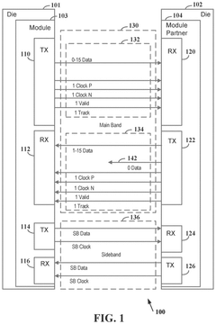
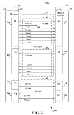
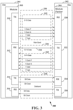
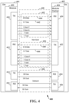
Variable link width in two directions for main band chip module connection
PatentPendingUS20240354279A1
Innovation
- Implementing a method to establish a die-to-die connection with a variable link width, allowing for independent configuration of transmit and receive data lanes through a sideband communication, enabling operation with different numbers of active data lanes in each direction to optimize power usage and data rates, and supporting fault tolerance by excluding faulty lines.
Die-to-die interconnect
PatentPendingCN117651940A
Innovation
- Using the Universal Chiplet Interconnect Express (UCIe) protocol, this protocol provides a universal, open on-package interconnect standard that supports high bandwidth, low latency and high power efficiency inter-core connections through standardized dies to The die interface enables interoperability across suppliers and factories.
Manufacturing Process Considerations for UCIe Implementation
The implementation of Universal Chiplet Interconnect Express (UCIe) requires careful consideration of manufacturing processes to ensure optimal performance and yield. Advanced packaging technologies such as flip-chip bonding, through-silicon vias (TSVs), and micro-bumps are essential for UCIe implementation, each presenting unique challenges in the manufacturing workflow.
Bump pitch reduction is a critical factor in UCIe manufacturing, as it directly impacts interconnect density and overall chiplet integration capabilities. Current industry standards for high-volume manufacturing typically achieve bump pitches of 40-55μm, while leading-edge research demonstrates capabilities down to 25-30μm. The manufacturing processes must be precisely controlled to maintain consistent bump height and coplanarity across the die surface.
Surface preparation techniques significantly influence UCIe implementation success. Chemical-mechanical planarization (CMP) processes must achieve surface roughness values below 5nm RMS to ensure proper bump formation and adhesion. Additionally, under-bump metallization (UBM) layers require precise deposition control, typically utilizing physical vapor deposition (PVD) or electroplating techniques with thickness variations maintained within ±5%.
Temperature management during the manufacturing process presents another critical consideration. The coefficient of thermal expansion (CTE) mismatch between different materials can lead to mechanical stress and potential bump failures. Manufacturing processes typically employ thermal cycling tests between -40°C and 125°C to validate interconnect reliability, with specialized underfill materials helping to mitigate CTE-related stresses.
Alignment accuracy represents a fundamental manufacturing challenge for fine-pitch UCIe implementations. Advanced manufacturing equipment must achieve alignment precision better than ±1.5μm to ensure proper bump connections. This precision requirement drives the need for sophisticated optical alignment systems and feedback control mechanisms in the manufacturing line.
Contamination control constitutes a paramount concern in UCIe manufacturing environments. Particle counts must be maintained below Class 10 (ISO 4) standards, with specialized cleaning processes implemented before critical manufacturing steps. Even microscopic contaminants can significantly impact yield rates when working with bump pitches below 40μm.
Testing methodologies must evolve to accommodate the unique characteristics of UCIe implementations. Non-destructive testing approaches such as X-ray inspection, acoustic microscopy, and electrical parametric testing are increasingly integrated into the manufacturing workflow to identify defects early in the process, thereby improving overall yield rates and reducing manufacturing costs.
Cost-Performance Analysis of Chiplet Integration Technologies
The economic viability of chiplet integration technologies depends heavily on the balance between manufacturing costs and performance benefits. UCIe (Universal Chiplet Interconnect Express) represents a significant advancement in chiplet interconnection standards, but implementing this technology involves careful consideration of cost factors against performance gains.
Manufacturing costs for UCIe-based chiplet designs are influenced by several key factors. The bump pitch—the distance between adjacent interconnect bumps—directly impacts manufacturing complexity and yield rates. Finer bump pitches enable higher interconnect density and bandwidth but increase manufacturing challenges and costs. Current industry standards for UCIe implementations typically range from 25-55μm bump pitches, with each reduction in pitch size potentially increasing manufacturing costs by 15-30%.
Yield considerations represent another critical cost factor. As bump pitch decreases, the probability of defects during the manufacturing process increases exponentially. Industry data suggests that moving from a 55μm to a 35μm bump pitch can reduce yield rates by approximately 8-12%, significantly impacting overall production economics. These yield challenges are particularly pronounced in high-volume manufacturing environments where even small percentage decreases in yield translate to substantial cost implications.
The cost structure of chiplet integration also includes testing and packaging expenses. UCIe implementations require sophisticated testing methodologies to ensure proper interconnect functionality, adding approximately 5-10% to overall production costs. Advanced packaging technologies necessary for UCIe, such as silicon interposers or organic substrates with fine-line routing capabilities, contribute an additional 20-30% to the total cost structure compared to traditional monolithic designs.
When analyzing the performance benefits against these costs, UCIe-based designs demonstrate compelling advantages. The technology enables 2-3x higher bandwidth density compared to traditional package-level interconnects, with energy efficiency improvements of 25-35% per bit transferred. These performance gains translate directly to system-level improvements in data-intensive applications such as AI training and high-performance computing.
The economic inflection point—where increased costs are justified by performance gains—varies by application. For high-performance computing applications, the premium cost of UCIe implementation (typically 30-40% higher than traditional approaches) is often justified by the 2-3x performance improvement. However, for cost-sensitive consumer applications, the economic equation becomes more challenging, requiring careful optimization of bump pitch and other design parameters to achieve acceptable cost-performance ratios.
Unlock deeper insights with Patsnap Eureka Quick Research — get a full tech report to explore trends and direct your research. Try now!
Generate Your Research Report Instantly with AI Agent
Supercharge your innovation with Patsnap Eureka AI Agent Platform!