UCIe Chiplet Interconnect Cost Modeling And NRE Breakdown
SEP 1, 20259 MIN READ
Generate Your Research Report Instantly with AI Agent
Patsnap Eureka helps you evaluate technical feasibility & market potential.
UCIe Chiplet Technology Background and Objectives
Universal Chiplet Interconnect Express (UCIe) represents a significant advancement in semiconductor integration technology, emerging as a response to the increasing challenges of traditional monolithic chip scaling. The evolution of chiplet technology can be traced back to the early 2010s when semiconductor manufacturers began exploring disaggregated chip designs to overcome the limitations imposed by Moore's Law. UCIe, officially introduced in March 2022, stands as a collaborative industry effort to standardize die-to-die interconnects for chiplet-based designs.
The primary objective of UCIe technology is to establish an open, industry-standard interconnect architecture that enables heterogeneous integration of chiplets from different vendors within a single package. This standardization aims to create a more flexible and cost-effective approach to semiconductor design and manufacturing, allowing companies to mix and match chiplets based on specific performance, power, and area requirements without being constrained by proprietary interconnect technologies.
UCIe technology addresses several critical challenges in modern semiconductor development. As traditional node scaling becomes increasingly difficult and expensive, chiplet-based designs offer an alternative path to continue performance scaling. By disaggregating complex SoCs into smaller, more manageable chiplets, manufacturers can optimize each component independently, potentially improving yields and reducing overall costs.
The technical evolution of chiplet interconnects has progressed through several generations, from early proprietary solutions like AMD's Infinity Fabric and Intel's EMIB to more standardized approaches. UCIe represents the culmination of these efforts, incorporating lessons learned from previous implementations while establishing a framework for future innovation. The standard encompasses both package-level interconnects and die-to-die interfaces, supporting both standard and advanced packaging technologies.
Current UCIe specifications define two primary interface layers: the Physical Layer and the Protocol Layer. The Physical Layer addresses signal integrity, power delivery, and mechanical aspects of chiplet integration, while the Protocol Layer focuses on data transfer protocols, error handling, and flow control mechanisms. Together, these specifications aim to ensure reliable, high-bandwidth, and low-latency communication between chiplets.
The long-term vision for UCIe technology extends beyond current implementations, with roadmaps indicating future support for higher bandwidth densities, improved power efficiency, and enhanced security features. As the ecosystem matures, UCIe is expected to enable more complex heterogeneous integration scenarios, potentially revolutionizing how semiconductor products are designed, manufactured, and brought to market.
Market Demand Analysis for Chiplet-Based Solutions
The chiplet market is experiencing unprecedented growth, driven by the increasing demand for high-performance computing solutions across various industries. As traditional monolithic chip designs reach their physical and economic limits, chiplet-based architectures have emerged as a compelling alternative. Market research indicates that the global chiplet market is projected to grow at a compound annual growth rate of 38% from 2023 to 2030, reaching a market value of 47 billion USD by 2030.
The primary market demand for UCIe chiplet interconnect technology stems from data centers and cloud service providers seeking to optimize performance while managing power consumption and costs. These entities require increasingly powerful computing solutions to handle artificial intelligence, machine learning, and big data analytics workloads. The chiplet approach allows for more efficient scaling of computing resources compared to traditional monolithic designs.
Consumer electronics manufacturers represent another significant market segment, as they seek to incorporate advanced computing capabilities into smaller form factors while maintaining reasonable power consumption profiles. The modular nature of chiplet-based designs enables more flexible product development and potentially faster time-to-market for new devices.
Telecommunications equipment providers are also driving demand for chiplet solutions as they deploy 5G infrastructure and prepare for future network technologies. These applications require high-bandwidth, low-latency processing capabilities that can be efficiently delivered through chiplet architectures.
Market analysis reveals that cost considerations are paramount for potential adopters of chiplet technology. While the initial non-recurring engineering (NRE) costs for chiplet designs may be higher than traditional approaches, the long-term total cost of ownership can be significantly lower due to improved yield rates, reusability of chiplet components, and reduced material waste.
Industry surveys indicate that 78% of semiconductor companies are actively exploring or implementing chiplet-based designs, with cost modeling being a critical factor in their decision-making process. The ability to accurately predict both NRE costs and production economics is essential for widespread adoption of UCIe chiplet interconnect technology.
Regional market analysis shows that North America currently leads in chiplet technology adoption, followed by Asia-Pacific and Europe. However, the Asia-Pacific region is expected to show the highest growth rate over the next five years as manufacturing capabilities expand and local demand increases for advanced computing solutions.
Current State and Challenges in Chiplet Interconnect
The UCIe (Universal Chiplet Interconnect Express) standard represents a significant advancement in chiplet interconnect technology, currently adopted by major industry players including Intel, AMD, TSMC, and Samsung. This open standard aims to establish a unified die-to-die interconnect protocol across the semiconductor industry. Despite its promising potential, UCIe faces several technical and economic challenges that impact its widespread implementation.
Current market analysis indicates that while chiplet technology offers substantial benefits in terms of manufacturing yield and design flexibility, the interconnect costs remain a significant portion of the overall chiplet implementation expenses. Industry data suggests that die-to-die interconnect can account for 20-30% of the total chiplet solution cost, with UCIe implementations varying based on implementation complexity and production volume.
A primary technical challenge for UCIe adoption lies in the physical implementation requirements. The standard demands precise alignment between chiplets, with bump pitches as small as 25-40μm for advanced packages. This necessitates specialized equipment and processes that increase manufacturing complexity and cost. Additionally, the testing infrastructure for UCIe connections requires sophisticated methodologies to ensure signal integrity across the interconnect, further adding to the non-recurring engineering (NRE) costs.
Thermal management presents another significant challenge. As chiplets are packed more densely, heat dissipation becomes increasingly problematic, particularly at the high data rates (up to 32 GT/s) supported by UCIe. Current cooling solutions often add complexity and cost to the overall package design, impacting both performance and economic viability.
From a geographical perspective, UCIe technology development is concentrated primarily in North America, East Asia, and to a lesser extent, Europe. This distribution creates potential supply chain vulnerabilities and regional disparities in adoption rates. The concentration of advanced packaging capabilities in specific regions also impacts the global accessibility of UCIe implementation resources.
Signal integrity challenges increase exponentially with higher data rates, requiring sophisticated equalization techniques and careful power delivery network design. Current UCIe implementations must balance performance requirements with power consumption constraints, often necessitating complex trade-offs that impact overall system efficiency.
The ecosystem maturity represents another significant hurdle. While the UCIe consortium has established the standard, the supporting design tools, IP blocks, and verification methodologies are still evolving. This immature ecosystem increases development risk and potentially extends time-to-market for products utilizing UCIe technology.
Current UCIe Implementation Approaches
01 Cost reduction strategies for UCIe chiplet interconnects
Various strategies can be implemented to reduce the cost of UCIe chiplet interconnects. These include optimizing manufacturing processes, using standardized interfaces, implementing efficient packaging techniques, and reducing material costs. By adopting these strategies, manufacturers can achieve cost-effective production of chiplet-based systems while maintaining high performance and reliability.- Cost reduction through advanced packaging technologies: UCIe chiplet interconnect costs can be reduced through advanced packaging technologies that optimize the integration of multiple chiplets. These technologies include the use of silicon interposers, organic substrates, and through-silicon vias (TSVs) that enable more efficient connections between chiplets. By improving the packaging architecture, manufacturers can decrease the overall production costs while maintaining high performance and reliability of the chiplet-based systems.
- Manufacturing process optimization for UCIe implementation: Optimizing manufacturing processes specifically for UCIe chiplet interconnects can significantly impact costs. This includes developing specialized fabrication techniques, improving yield rates, and implementing more efficient testing methodologies. By streamlining the manufacturing workflow and reducing defect rates, the overall cost of producing UCIe-compliant chiplets can be decreased, making the technology more accessible for various applications.
- Power efficiency improvements to reduce operational costs: Enhancing the power efficiency of UCIe chiplet interconnects can lead to reduced operational costs over the lifetime of the system. This involves implementing advanced power management techniques, optimizing signal integrity, and reducing power consumption during data transfer between chiplets. These improvements not only decrease the energy requirements but also reduce thermal management needs, resulting in lower overall system costs.
- Standardization and interoperability to reduce design costs: The standardization of UCIe specifications and ensuring interoperability between different vendors' chiplets can significantly reduce design and integration costs. By establishing common protocols, interface specifications, and testing methodologies, companies can avoid custom development expenses and leverage existing designs. This approach enables a more competitive ecosystem where chiplets from various manufacturers can work together seamlessly, driving down overall system costs.
- Scaling and miniaturization strategies for cost efficiency: Implementing scaling and miniaturization strategies for UCIe chiplet interconnects can lead to improved cost efficiency. This includes reducing die sizes, optimizing interconnect densities, and developing more compact packaging solutions. By maximizing the number of functional units per wafer and minimizing material usage, manufacturers can achieve better economies of scale and lower per-unit costs while maintaining the performance benefits of chiplet-based designs.
02 Advanced packaging technologies for UCIe implementation
Advanced packaging technologies play a crucial role in implementing UCIe chiplet interconnects cost-effectively. These technologies include 2.5D and 3D integration, silicon interposers, and organic substrates. By utilizing these advanced packaging approaches, manufacturers can optimize the physical implementation of UCIe interfaces, resulting in improved performance and reduced overall system costs.Expand Specific Solutions03 Manufacturing yield improvements for UCIe chiplets
Improving manufacturing yields is essential for reducing the cost of UCIe chiplet interconnects. Techniques such as design for manufacturability, process optimization, defect detection, and redundancy implementation can significantly enhance yields. Higher yields translate to lower production costs, making chiplet-based designs more economically viable compared to monolithic approaches.Expand Specific Solutions04 Economic analysis of UCIe versus traditional interconnect technologies
Economic comparisons between UCIe chiplet interconnects and traditional interconnect technologies reveal potential cost advantages. Factors considered in this analysis include design flexibility, reusability of IP blocks, time-to-market, and scaling benefits. The modular nature of chiplet designs allows for more efficient use of silicon area and potentially lower overall system costs despite the additional interconnect overhead.Expand Specific Solutions05 Standardization impact on UCIe chiplet interconnect costs
The standardization of UCIe chiplet interconnects has significant implications for cost reduction. Industry-wide adoption of standardized interfaces enables ecosystem development, promotes competition among suppliers, and facilitates interoperability between chiplets from different vendors. This standardization reduces design and validation costs, simplifies integration, and creates economies of scale that drive down the overall cost of chiplet-based systems.Expand Specific Solutions
Key Industry Players in Chiplet Ecosystem
The UCIe Chiplet Interconnect market is currently in its early growth phase, characterized by rapid technological advancement and increasing industry adoption. The market size is projected to expand significantly as chiplet technology becomes essential for next-generation computing architectures. From a technical maturity perspective, industry leaders Intel and AMD (through Xilinx acquisition) are spearheading standardization efforts, while Qualcomm, Samsung, and Huawei are making substantial investments in chiplet interconnect technologies. Western Digital and Microchip are developing complementary storage and peripheral integration solutions. The competitive landscape shows a clear division between established semiconductor giants with extensive IP portfolios and emerging specialized players focusing on specific aspects of the UCIe ecosystem. Cost modeling remains a critical challenge as companies work to optimize the NRE-to-volume production ratio while maintaining performance advantages over traditional monolithic designs.
QUALCOMM, Inc.
Technical Solution: Qualcomm has developed a sophisticated approach to UCIe chiplet interconnect cost modeling focused on mobile and edge computing applications. Their methodology incorporates both die-to-die (D2D) and die-to-wafer (D2W) integration scenarios, with particular emphasis on power efficiency metrics that impact overall system costs. Qualcomm's cost models factor in their proprietary High-Speed Low-Power (HSLP) interface technology, which has been adapted to align with UCIe standards while maintaining backward compatibility with their existing interconnect solutions. Their NRE breakdown typically allocates 35-45% to architecture and design, 20-30% to verification and validation, 15-20% to software development and integration, and the remainder to certification and compliance testing. Qualcomm has demonstrated that their chiplet-based approach can reduce development costs by approximately 30% for iterative product generations by enabling IP block reuse across multiple product lines. Their cost modeling also incorporates sophisticated yield analysis that accounts for known good die (KGD) testing and advanced packaging yield factors, which they claim can improve overall economics by 15-25% compared to traditional SoC approaches for certain applications.
Strengths: Qualcomm's expertise in power-efficient designs translates to cost advantages in thermal management and packaging. Their established mobile ecosystem provides valuable real-world cost data. Weaknesses: Their cost models may be overly optimized for mobile applications, potentially limiting applicability to high-performance computing scenarios. Dependency on third-party manufacturing may introduce additional cost variables.
Intel Corp.
Technical Solution: Intel has pioneered UCIe (Universal Chiplet Interconnect Express) as a founding member of the UCIe consortium. Their approach to chiplet interconnect cost modeling involves a comprehensive framework that addresses both physical and protocol layers. Intel's Embedded Multi-die Interconnect Bridge (EMIB) technology serves as a foundation for their UCIe implementation, providing high-bandwidth, low-latency die-to-die connections without the need for silicon interposers. Their cost modeling accounts for various factors including silicon area, packaging complexity, testing overhead, and yield implications. Intel has reported that their advanced packaging technologies can reduce costs by up to 40% compared to monolithic designs for certain applications. The NRE (Non-Recurring Engineering) breakdown in Intel's model typically includes design costs (approximately 30-40%), validation and testing (25-30%), IP licensing (10-15%), and tooling setup (remaining percentage). Intel's Advanced Interface Bus (AIB) protocol, which aligns with UCIe standards, enables a modular approach to chip design that can significantly reduce development cycles and associated NRE costs.
Strengths: Intel's extensive manufacturing infrastructure provides vertical integration advantages in cost optimization. Their established ecosystem allows for better economies of scale. Weaknesses: Their cost models may be optimized for their own manufacturing processes, potentially limiting applicability to other fabrication approaches. Higher initial investment requirements compared to some competitors.
Core Patents and Technical Literature in Chiplet Interconnect
On-package memory with universal chiplet interconnect express
PatentPendingUS20250123990A1
Innovation
- The implementation of Universal Chiplet Interconnect Express (UCIe) enhances memory interfacing by standardizing connections between processors and various memory types, optimizing communication, and integrating memory controllers on the same package to increase bandwidth and reduce latency.
Reconfigurable circuit, device for interconnecting reconfigurable chips and method thereof
PatentActiveCN117056279B
Innovation
- A reconfigurable circuit is designed, including a reconfigurable interconnect module and a control module, connected to the micro-bump group through multiple reconfigurable switch units, and controlled by a non-volatile memory module and a register group module to realize the chip Flexible connections and multiple reconfigurations between particles.
Cost Structure Breakdown and NRE Analysis
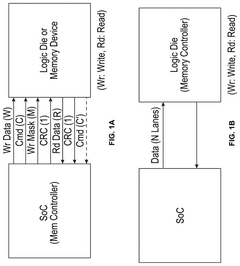
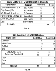
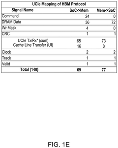
The cost structure of UCIe (Universal Chiplet Interconnect Express) implementation can be divided into several key components that significantly impact the overall economics of chiplet-based designs. The primary cost elements include silicon area, packaging technology, testing infrastructure, and intellectual property licensing. Silicon area costs are directly proportional to the die size dedicated to UCIe interfaces, which typically ranges from 0.5mm² to 2mm² depending on the implementation complexity and bandwidth requirements.
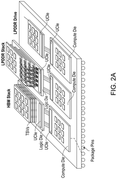
Packaging costs represent approximately 30-40% of the total chiplet implementation expenses, with advanced packaging technologies like silicon interposers and organic substrates commanding premium pricing. The choice between fan-out wafer-level packaging (FOWLP) and 2.5D/3D integration significantly influences the cost structure, with more advanced solutions potentially doubling the packaging expenses.
Testing infrastructure costs account for 15-25% of the total implementation budget, encompassing both pre-packaging die testing and post-packaging system validation. The specialized equipment required for high-speed interface testing at UCIe's 16-32 GT/s data rates represents a substantial capital investment for manufacturers.
Non-recurring engineering (NRE) costs for UCIe implementation can be broken down into several categories. Design and verification expenses typically constitute 40-50% of total NRE, covering the architectural planning, circuit design, and extensive simulation required to ensure compliance with the UCIe specification. These costs range from $5-15 million depending on design complexity and performance targets.
Mask generation and initial production setup represent another 20-30% of NRE costs, with advanced nodes (5nm and below) significantly increasing these expenses compared to mature process technologies. Test development accounts for 15-20% of NRE investment, encompassing the creation of specialized test vectors and validation methodologies specific to chiplet interfaces.
Certification and compliance testing contribute the remaining 10-15% of NRE expenses, ensuring interoperability with other UCIe-compliant components. This includes formal verification against the UCIe standard and interoperability testing with reference designs. The total NRE investment for a comprehensive UCIe implementation typically ranges from $10-30 million, with higher costs associated with leading-edge process nodes and more complex implementations targeting maximum bandwidth configurations.
Supply Chain Considerations for UCIe Implementation
The implementation of UCIe (Universal Chiplet Interconnect Express) technology requires careful consideration of supply chain dynamics to ensure successful adoption and cost-effective manufacturing. The current semiconductor supply chain is highly specialized, with different entities focusing on specific aspects of the production process, from design to packaging and testing.
For UCIe implementation, organizations must evaluate their existing supply chain partnerships and potentially establish new relationships with specialized vendors. Key supply chain considerations include the availability of advanced packaging facilities capable of handling chiplet integration with the precision required by UCIe specifications. Currently, only a limited number of foundries and OSATs (Outsourced Semiconductor Assembly and Test) providers possess the technical capabilities to support UCIe-based designs.
Material sourcing represents another critical supply chain factor. UCIe implementations require specific substrate materials and interconnect technologies that may have limited supplier options. Organizations must secure reliable sources for these specialized materials to avoid production bottlenecks and ensure consistent quality across manufacturing runs.
The geographical distribution of the UCIe supply chain introduces additional complexities. With key suppliers concentrated in specific regions, particularly East Asia, companies must develop strategies to mitigate geopolitical risks and potential supply disruptions. Diversification of supply sources, where possible, can help address these concerns, though this may come with increased coordination costs.
Intellectual property management across the supply chain presents unique challenges for UCIe implementation. As chiplet designs may incorporate IP from multiple vendors, clear agreements regarding IP ownership, licensing, and protection must be established throughout the supply chain. This is particularly important given the modular nature of chiplet-based designs, where different components may originate from different suppliers.
Testing and validation capabilities within the supply chain also warrant attention. UCIe implementations require specialized testing procedures to verify proper die-to-die communication and overall system functionality. Organizations must ensure their supply chain partners possess the necessary testing equipment and expertise to support these requirements.
Finally, supply chain transparency and traceability are increasingly important considerations for UCIe implementation. As chiplet-based designs involve multiple suppliers and manufacturing steps, maintaining visibility throughout the production process helps identify potential quality issues and ensures compliance with industry standards and regulatory requirements.
Unlock deeper insights with Patsnap Eureka Quick Research — get a full tech report to explore trends and direct your research. Try now!
Generate Your Research Report Instantly with AI Agent
Supercharge your innovation with Patsnap Eureka AI Agent Platform!