Packaging Warpage Control For UCIe Chiplet Interconnect
SEP 1, 20259 MIN READ
Generate Your Research Report Instantly with AI Agent
Patsnap Eureka helps you evaluate technical feasibility & market potential.
UCIe Chiplet Packaging Warpage Background and Objectives
The Universal Chiplet Interconnect Express (UCIe) has emerged as a transformative technology in the semiconductor industry, enabling heterogeneous integration of multiple chiplets within a single package. This approach represents a paradigm shift from traditional monolithic chip designs to more modular architectures, allowing for improved performance, power efficiency, and manufacturing yield. The evolution of chiplet technology has been driven by the slowing of Moore's Law and the increasing challenges in scaling traditional integrated circuits.
Warpage control has become a critical challenge in UCIe chiplet packaging. As the industry moves toward more complex multi-chiplet designs with finer interconnect pitches, even minor package warpage can significantly impact the reliability of die-to-die connections. Historically, package warpage was manageable with larger interconnect pitches, but UCIe's sub-micron pitch requirements have dramatically tightened warpage tolerances.
The technical evolution of warpage control spans several decades, beginning with simple single-chip packages and progressing through various integration approaches including multi-chip modules (MCMs), 2.5D integration with silicon interposers, and now advanced chiplet architectures. Each evolutionary step has introduced more stringent warpage requirements, with UCIe representing the most demanding standard to date.
Current UCIe specifications demand warpage control within extremely tight tolerances—typically less than 20 microns across the package—to ensure reliable interconnections between chiplets. This precision is necessary to maintain the integrity of the thousands of interconnects that may exist between adjacent chiplets, each requiring perfect alignment during the bonding process.
The primary objective of warpage control in UCIe packaging is to ensure consistent, reliable electrical connections between chiplets while maintaining manufacturing yield at economically viable levels. This involves developing materials, processes, and design methodologies that can predictably manage the complex thermomechanical interactions within heterogeneous packages.
Secondary objectives include minimizing the cost impact of warpage control measures, ensuring compatibility with existing manufacturing infrastructure, and developing solutions that can scale with future generations of the UCIe standard as interconnect densities continue to increase.
The industry is currently witnessing a convergence of materials science, mechanical engineering, and electronic design automation to address these challenges, with significant research focused on coefficient of thermal expansion (CTE) matching, novel substrate materials, and advanced simulation techniques to predict and mitigate warpage effects throughout the product lifecycle.
Market Demand Analysis for Advanced Chiplet Interconnect Solutions
The global market for advanced chiplet interconnect solutions is experiencing robust growth, driven by the increasing demand for high-performance computing systems across various industries. The Universal Chiplet Interconnect Express (UCIe) standard has emerged as a critical technology enabler for heterogeneous integration, allowing semiconductor companies to mix and match chiplets from different vendors while maintaining high-speed, low-latency communication between components.
Market research indicates that the chiplet market is projected to grow at a compound annual growth rate of over 40% through 2027, with the total addressable market expected to reach several billion dollars. This growth is primarily fueled by data centers, artificial intelligence applications, and high-performance computing sectors that require increasingly powerful and energy-efficient solutions that traditional monolithic chip designs struggle to deliver.
The demand for UCIe-based solutions is particularly strong in cloud service providers and hyperscalers who are seeking to optimize their infrastructure for workloads like machine learning training and inference. These customers value the flexibility of chiplet-based designs that allow for customization while reducing development costs and time-to-market compared to fully custom ASICs.
Packaging warpage control represents a critical factor in the commercial viability of UCIe implementations. Industry surveys reveal that yield issues related to warpage can increase manufacturing costs by 15-30%, significantly impacting the economic advantages of chiplet-based designs. Customers across the semiconductor ecosystem have expressed strong interest in solutions that can mitigate these challenges.
Geographically, North America leads in demand for advanced chiplet interconnect solutions, followed by East Asia, particularly Taiwan, South Korea, and Japan where major semiconductor manufacturing is concentrated. Europe shows growing interest, especially in automotive and industrial applications where reliability under thermal stress is paramount.
The market segmentation reveals distinct customer profiles: high-performance computing and data center operators prioritize bandwidth and power efficiency; telecommunications equipment manufacturers focus on reliability and standardization; while consumer electronics companies emphasize cost-effectiveness and miniaturization capabilities.
Customer feedback indicates that solving packaging warpage issues could accelerate UCIe adoption by 18-24 months across these segments. Specifically, thermal management solutions that address coefficient of thermal expansion (CTE) mismatches between different materials in the package stack are highly sought after, as they directly impact manufacturing yield, long-term reliability, and overall system performance.
Current Warpage Control Challenges in UCIe Implementation
The implementation of Universal Chiplet Interconnect Express (UCIe) faces significant warpage control challenges that threaten the reliability and performance of chiplet-based architectures. The primary challenge stems from the thermal expansion coefficient (CTE) mismatch between different materials used in the package assembly. When silicon dies with low CTE values are attached to organic substrates with higher CTE values, the package experiences differential expansion and contraction during thermal cycling, resulting in warpage that can compromise the fine-pitch interconnects required by UCIe standards.
The ultra-fine pitch requirements of UCIe (down to 25μm bump pitch) create an extremely narrow tolerance window for warpage. Even minor deviations can lead to connection failures, as the physical margin for error is significantly reduced compared to traditional packaging technologies. This challenge is particularly acute during the reflow soldering process, where temperature variations can cause dynamic warpage that exceeds acceptable limits.
Another critical challenge is the increasing die-to-die proximity demanded by UCIe implementations. As chiplets are placed closer together to minimize latency and maximize bandwidth, the gap between adjacent dies becomes smaller, leaving minimal space for warpage accommodation. This proximity requirement conflicts directly with the natural tendency of packages to warp under thermal stress, creating a fundamental engineering dilemma.
Multi-layer packages with varying material properties compound the warpage issue. Each material layer in the stack-up contributes differently to the overall warpage behavior, making prediction and control increasingly complex. The interaction between these layers during thermal cycling creates non-linear warpage patterns that are difficult to model accurately using conventional simulation tools.
Manufacturing process variations introduce additional uncertainty in warpage control. Inconsistencies in material properties, adhesive application, curing conditions, and assembly pressures can all contribute to unpredictable warpage outcomes. This variability makes it challenging to establish reliable manufacturing processes that consistently produce packages meeting UCIe warpage specifications.
The industry also faces measurement challenges when dealing with UCIe-level warpage control. Traditional warpage measurement techniques lack the resolution and accuracy needed to characterize the minute deformations that can affect UCIe interconnect reliability. Real-time measurement during thermal cycling presents additional technical hurdles that must be overcome to develop effective warpage control strategies.
Cost considerations further complicate warpage control solutions. While advanced substrate materials with tailored CTE values could mitigate warpage issues, their higher cost impacts the economic viability of UCIe implementations. Similarly, sophisticated warpage compensation techniques often require expensive equipment and process steps that must be balanced against the performance benefits they provide.
Current Warpage Mitigation Strategies for Chiplet Packaging
01 Warpage control in chiplet packaging
Various methods are employed to control warpage in chiplet packaging with UCIe interconnects. These include using specific substrate materials with matched coefficients of thermal expansion, implementing stress-relieving structures, and optimizing the package design to distribute stress evenly. These techniques help maintain the planarity of the package during thermal cycling, which is critical for reliable UCIe interconnections between chiplets.- Warpage control in UCIe chiplet packaging: Various methods are employed to control warpage in UCIe (Universal Chiplet Interconnect Express) chiplet packaging. These include using specific substrate materials with matched coefficient of thermal expansion (CTE), implementing stress compensation layers, and optimizing the package design to distribute stress evenly. Advanced simulation techniques are used to predict and mitigate warpage during thermal cycling, ensuring reliable interconnections between chiplets.
- Thermal management solutions for chiplet interconnects: Thermal management is critical in UCIe chiplet packaging to prevent warpage and ensure reliable interconnections. Solutions include integrating thermal interface materials between chiplets, incorporating heat spreaders and heat sinks, and designing thermal vias in the substrate. Advanced cooling techniques such as microfluidic cooling channels and phase-change materials are also implemented to manage heat distribution and minimize thermal-induced stress.
- Advanced materials for UCIe packaging warpage reduction: Specialized materials are developed to address warpage challenges in UCIe chiplet packaging. These include low-CTE substrate materials, composite underfills with enhanced mechanical properties, and novel die-attach materials that can absorb stress. Reinforced polymers and ceramic-based substrates with tailored thermal and mechanical properties help maintain package flatness during assembly and operation, ensuring reliable high-density interconnections.
- Manufacturing processes to minimize interconnect warpage: Optimized manufacturing processes are essential to minimize warpage in UCIe chiplet packaging. These include controlled reflow profiles, sequential assembly techniques, and precision placement methods. Advanced molding compounds and encapsulation processes are designed to balance internal stresses. Post-assembly treatments such as annealing and stress relief processes help maintain package flatness and ensure reliable electrical connections between chiplets.
- Testing and quality control for UCIe chiplet interconnects: Comprehensive testing and quality control methods are implemented to ensure UCIe chiplet interconnects maintain integrity despite potential warpage. These include optical and mechanical warpage measurement techniques, in-situ monitoring during thermal cycling, and electrical testing of interconnects under stress conditions. Advanced imaging technologies such as X-ray and acoustic microscopy are used to detect delamination or microcracks that might affect interconnect reliability.
02 Thermal management solutions for UCIe chiplet interconnects
Thermal management is crucial in UCIe chiplet packaging to prevent warpage. Solutions include integrated heat spreaders, thermal interface materials with specific properties, and advanced cooling mechanisms. These thermal management approaches help maintain consistent temperatures across the package, reducing thermal gradients that can lead to warpage and ensuring the reliability of the fine-pitch interconnects used in UCIe technology.Expand Specific Solutions03 Advanced materials for UCIe packaging warpage reduction
Specialized materials are developed to address warpage in UCIe chiplet packaging. These include composite substrates, low-CTE (Coefficient of Thermal Expansion) materials, and novel underfill formulations. The materials are designed to minimize stress during manufacturing processes and operation, providing dimensional stability for the high-density interconnects required in UCIe implementations.Expand Specific Solutions04 Manufacturing processes to minimize warpage in UCIe implementations
Specific manufacturing processes are developed to minimize warpage in UCIe chiplet packaging. These include controlled reflow profiles, sequential assembly techniques, and precision molding processes. Process optimization focuses on maintaining alignment during the critical interconnection steps, ensuring that the fine-pitch UCIe interfaces remain properly aligned despite thermal and mechanical stresses during manufacturing.Expand Specific Solutions05 Testing and simulation methods for UCIe packaging warpage
Advanced testing and simulation methods are employed to predict and measure warpage in UCIe chiplet packaging. These include finite element analysis, shadow moiré techniques, digital image correlation, and in-situ warpage measurement during assembly. These methods help optimize package designs before manufacturing and validate the effectiveness of warpage control strategies, ensuring reliable UCIe interconnections in the final product.Expand Specific Solutions
Key Industry Players in UCIe Chiplet Ecosystem
The UCIe chiplet interconnect packaging warpage control market is in its early growth phase, characterized by increasing adoption of advanced packaging technologies for heterogeneous integration. The market is expanding rapidly as chiplet architectures become essential for high-performance computing applications, with projections indicating significant growth over the next five years. Leading semiconductor companies including Intel, TSMC, AMD, and Samsung are driving technological innovation in this space, with Intel particularly advancing UCIe standardization efforts. Packaging specialists like JCET Group, Powertech Technology, and STATS ChipPAC are developing specialized warpage control solutions. The technology is approaching maturity for first-generation implementations, though challenges remain in ultra-fine pitch interconnects and thermal management for high-density chiplet designs.
Intel Corp.
Technical Solution: Intel has developed comprehensive warpage control solutions for UCIe chiplet interconnects, focusing on advanced material selection and structural optimization. Their approach includes using low-CTE (Coefficient of Thermal Expansion) substrate materials and implementing strategic stiffener designs to minimize warpage during thermal cycling. Intel's Embedded Multi-die Interconnect Bridge (EMIB) technology complements their UCIe implementation by providing precise die-to-die connections while controlling warpage through optimized bridge structures. They've also pioneered thermal compression bonding techniques specifically calibrated for UCIe applications, ensuring uniform pressure distribution during assembly to prevent warpage-induced connection failures. Intel's simulation-driven design methodology incorporates multi-physics modeling that predicts warpage behavior across the entire temperature range experienced during manufacturing and operation.
Strengths: Intel's extensive manufacturing infrastructure allows for rapid iteration and validation of warpage control techniques. Their vertical integration enables coordinated optimization across chip design, packaging, and assembly processes. Weaknesses: Their solutions may be optimized primarily for x86 architecture implementations, potentially limiting applicability to other semiconductor platforms. Higher implementation costs compared to simpler packaging approaches.
Huawei Technologies Co., Ltd.
Technical Solution: Huawei has developed a multi-layered approach to UCIe chiplet warpage control centered around their advanced Kirin chip architecture. Their solution incorporates gradient-stiffness substrate designs where material composition varies across the package to counteract warpage forces during thermal cycling. Huawei employs proprietary molding compound formulations with carefully engineered viscoelastic properties that provide dynamic warpage compensation throughout temperature fluctuations. Their manufacturing process includes precision-controlled cooling profiles during assembly that minimize residual stresses. Huawei has also implemented real-time optical measurement systems during production that allow for adaptive process control based on actual warpage measurements, enabling corrective actions during manufacturing. Their approach integrates machine learning algorithms that analyze historical warpage data to optimize design parameters for new chiplet configurations.
Strengths: Huawei's solution demonstrates excellent performance in high-density applications where multiple chiplets must maintain precise alignment. Their integrated measurement and control systems enable consistent quality across high-volume manufacturing. Weaknesses: Reliance on proprietary materials may create supply chain vulnerabilities. The complexity of their multi-layered approach requires sophisticated manufacturing equipment and expertise.
Critical Patents and Research in UCIe Warpage Control
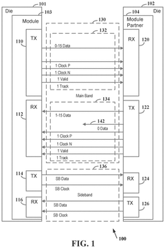
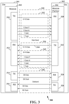
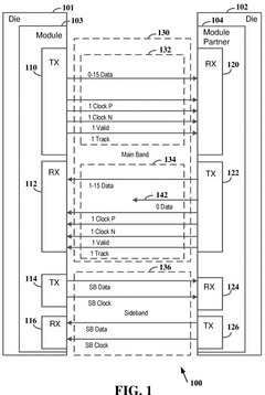
Variable link width in two directions for main band chip module connection
PatentPendingUS20240354279A1
Innovation
- Implementing a method to establish a die-to-die connection with a variable link width, allowing for independent configuration of transmit and receive data lanes through a sideband communication, enabling operation with different numbers of active data lanes in each direction to optimize power usage and data rates, and supporting fault tolerance by excluding faulty lines.
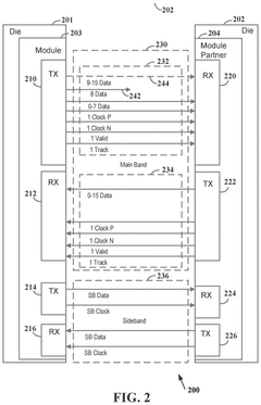
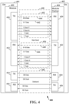
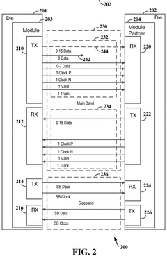
Variable link width in two directions for main band chip module connection
PatentWO2024226177A1
Innovation
- Implementing a variable link width mechanism in both directions of the main band connection, allowing for dynamic adjustment of the number of active data lanes based on requirements through a sideband communication protocol, enabling independent configuration of transmit and receive data lines to optimize power usage and data rates.

Thermal Management Considerations in UCIe Packaging
Thermal management represents a critical aspect of UCIe (Universal Chiplet Interconnect Express) packaging design, particularly when addressing warpage control challenges. The high-density interconnects in UCIe packages generate significant heat during operation, with thermal densities often exceeding 100W/cm² in advanced applications. This concentrated heat generation creates thermal gradients that directly contribute to package warpage through differential thermal expansion.
The coefficient of thermal expansion (CTE) mismatch between different materials in UCIe packages exacerbates warpage issues. Silicon chiplets typically have a CTE of 2-3 ppm/°C, while organic substrates range from 15-18 ppm/°C, creating substantial stress at interface regions during thermal cycling. These thermal-mechanical interactions must be carefully managed to maintain the precise alignment required for UCIe's fine-pitch interconnects.
Thermal design power (TDP) considerations significantly impact warpage control strategies. Higher-performance chiplets with elevated TDP values require more robust thermal management solutions, which often introduce additional materials and interfaces that must be accounted for in warpage mitigation. The thermal solution itself—whether direct lid contact, thermal interface materials, or integrated heat spreaders—introduces mechanical forces that can either counteract or worsen warpage tendencies.
Dynamic thermal conditions present particular challenges for UCIe packages. Power-state transitions during operation create transient thermal gradients that induce momentary warpage fluctuations. These dynamic effects can temporarily disrupt the electrical integrity of chiplet interconnects, especially in packages utilizing silicon bridges or interposers where alignment tolerances are extremely tight.
Advanced thermal simulation techniques have become essential for predicting and controlling warpage in UCIe implementations. Coupled thermal-mechanical finite element analysis (FEA) enables designers to model the complex interactions between thermal loads and mechanical responses across multiple materials and interfaces. These simulations inform material selection, geometry optimization, and thermal solution design to minimize warpage effects.
Innovative thermal management approaches specifically targeting warpage control include embedded cooling channels, thermally optimized underfill materials, and strategic thermal interface material (TIM) placement. These solutions aim to create more uniform temperature distributions across the package, reducing the thermal gradients that drive warpage. Some advanced designs incorporate active thermal management systems that dynamically adjust cooling to maintain dimensional stability during varying workloads.
Materials Science Advancements for Improved Warpage Control
Recent advancements in materials science have significantly contributed to addressing warpage challenges in UCIe chiplet interconnect packaging. The development of novel composite materials with tailored coefficient of thermal expansion (CTE) properties has emerged as a critical innovation. These materials incorporate specialized fillers such as silica nanoparticles and carbon nanotubes that can be precisely engineered to match the CTE of silicon dies and organic substrates, thereby minimizing thermal stress during temperature cycling.
Thermally conductive adhesives with improved mechanical properties represent another breakthrough area. These next-generation adhesives not only provide excellent thermal management but also offer enhanced flexibility to accommodate differential expansion between package components. Some formulations incorporate phase-change materials that can absorb expansion-related stress during temperature fluctuations, maintaining structural integrity across the operating temperature range.
Mold compound innovations have focused on developing materials with reduced curing shrinkage and improved dimensional stability. Advanced epoxy formulations with modified curing chemistry demonstrate up to 40% reduction in warpage compared to conventional compounds. These materials incorporate stress-relieving additives that can dynamically respond to mechanical stresses during assembly and operation.
Substrate material advancements have yielded high-modulus, low-CTE alternatives to traditional organic substrates. Glass-reinforced composites with specialized resin systems provide exceptional dimensional stability while maintaining necessary electrical properties. Some manufacturers have developed gradient materials with spatially varying properties that can create a more gradual transition between silicon and organic components.
Surface treatment technologies have also evolved to enhance adhesion between dissimilar materials while accommodating differential movement. Plasma-activated bonding techniques and chemically modified interfaces create stronger yet more compliant bonds between package components. These treatments can be selectively applied to create regions of varying compliance within the package structure.
Underfill materials have seen significant innovation with the development of reworkable formulations that maintain mechanical integrity across broader temperature ranges. These materials incorporate self-healing mechanisms that can repair microcracks formed during thermal cycling, extending package reliability. Some advanced underfills feature anisotropic properties that allow for controlled expansion in specific directions to minimize overall warpage effects.
Unlock deeper insights with Patsnap Eureka Quick Research — get a full tech report to explore trends and direct your research. Try now!
Generate Your Research Report Instantly with AI Agent
Supercharge your innovation with Patsnap Eureka AI Agent Platform!