

UCIe Chiplet Interconnect Protocol Layers And Mapping Methods
SEP 1, 20259 MIN READ
Generate Your Research Report Instantly with AI Agent
PatSnap Eureka helps you evaluate technical feasibility & market potential.
UCIe Chiplet Technology Background and Objectives
Universal Chiplet Interconnect Express (UCIe) emerged as a critical technology in response to the growing challenges in semiconductor scaling and the increasing demand for heterogeneous integration. The evolution of chiplet technology can be traced back to the slowdown of Moore's Law, where traditional monolithic chip designs faced physical limitations and escalating manufacturing costs. As transistor scaling became more difficult, the industry began exploring alternative approaches to continue performance improvements while managing costs and power consumption.
The development of UCIe represents a significant milestone in this technological evolution, building upon earlier interconnect technologies such as Intel's EMIB (Embedded Multi-die Interconnect Bridge), AMD's Infinity Fabric, and TSMC's CoWoS (Chip on Wafer on Substrate). These predecessors demonstrated the viability of disaggregating complex systems into smaller, more manageable chiplets, but lacked standardization across the industry.
UCIe aims to establish an open, standardized die-to-die interconnect that enables chiplets from different vendors to work seamlessly together. This standardization is crucial for fostering innovation and competition in the semiconductor ecosystem, allowing specialized manufacturers to focus on their areas of expertise while ensuring interoperability.
The primary technical objectives of UCIe include achieving high bandwidth density (up to 2 Tbps/mm), low latency communication between chiplets, power efficiency, and scalability across different packaging technologies. The standard encompasses both the physical layer specifications and protocol layers necessary for reliable data transfer between chiplets.
UCIe's protocol architecture is organized into three distinct layers: the Physical Layer, which handles the electrical signaling; the Die-to-Die Adapter Layer, which manages flow control and reliability; and the Protocol Layer, which supports various standard protocols such as PCIe, CXL, and custom protocols.
The technology targets a wide range of applications, from high-performance computing and data centers to edge computing and mobile devices. By enabling mix-and-match chiplet designs, UCIe supports more efficient product development cycles and potentially reduces time-to-market for new semiconductor products.
Industry projections indicate that the chiplet market is expected to grow significantly, with estimates suggesting it could reach $50 billion by 2030. This growth is driven by the fundamental advantages chiplets offer: improved yield, reduced development costs, enhanced performance, and greater design flexibility compared to monolithic approaches.
The UCIe consortium, founded in 2022 with initial members including Intel, AMD, Arm, TSMC, Samsung, and other industry leaders, continues to expand its membership and refine the specification to address emerging technical challenges and market requirements.
Market Demand Analysis for Chiplet-Based Integration
The chiplet-based integration market is experiencing unprecedented growth, driven by the increasing complexity of semiconductor designs and the physical limitations of traditional monolithic approaches. As Moore's Law faces challenges, the semiconductor industry is pivoting toward disaggregated architectures that allow for more flexible, cost-effective, and performance-optimized solutions. The global chiplet market is projected to grow at a CAGR of 40% from 2023 to 2030, reaching significant market valuation by the end of the decade.
The primary demand drivers for UCIe (Universal Chiplet Interconnect Express) technology stem from several converging market forces. High-performance computing applications, including AI/ML workloads, require increasingly specialized silicon solutions that can be rapidly developed and deployed. These applications demand both high bandwidth and low latency interconnects between chiplets, which UCIe aims to standardize.
Data centers represent the largest immediate market opportunity, with hyperscalers actively investing in chiplet-based architectures to optimize performance per watt and reduce total cost of ownership. The need for customized solutions while maintaining economies of scale has created strong pull for standardized chiplet interfaces like UCIe.
Consumer electronics manufacturers are also showing interest in chiplet technology to enable more differentiated products with improved performance and power efficiency. The automotive sector, particularly for advanced driver-assistance systems and autonomous vehicles, represents another growing market segment requiring heterogeneous integration capabilities.
Market research indicates that approximately 65% of new high-performance system-on-chip designs will incorporate some form of chiplet-based architecture by 2026. This transition is accelerating as more companies join industry consortia like the UCIe Consortium to establish interoperability standards.
The economic benefits driving market demand include reduced development costs through IP reuse, improved manufacturing yields by limiting die sizes, and faster time-to-market through parallel development of different chiplet components. Additionally, the ability to mix process nodes allows companies to optimize cost-performance tradeoffs by using advanced nodes only where necessary.
Regional analysis shows North America leading in chiplet adoption, followed by Asia-Pacific with significant growth potential. The establishment of UCIe as a standardized protocol for chiplet interconnection is expected to accelerate market growth by reducing integration barriers and enabling a more diverse ecosystem of chiplet suppliers and integrators.
UCIe Protocol Layers: Current Status and Challenges
The Universal Chiplet Interconnect Express (UCIe) protocol stack represents a significant advancement in chiplet interconnection technology, yet faces several critical challenges in its current implementation. The protocol is structured in three distinct layers: Physical, Die-to-Die, and Protocol Adaptation Layers, each with its own set of technical complexities and development hurdles.
The Physical Layer (PHY) of UCIe currently supports both Standard and Advanced modes, operating at 16 GT/s and 32 GT/s respectively. While these speeds represent substantial improvements over previous interconnect technologies, they still lag behind the theoretical bandwidth capabilities needed for next-generation computing applications. Signal integrity issues at these high speeds remain a persistent challenge, particularly when dealing with varying chiplet distances and substrate materials.
In the Die-to-Die Layer (D2D), the protocol implements flow control mechanisms and error handling that, while functional, introduce latency penalties that can impact overall system performance. Current implementations struggle with efficient power management across different operational states, leading to suboptimal energy consumption profiles when scaling to larger chiplet configurations.
The Protocol Adaptation Layer (PAL) faces perhaps the most significant challenges, as it must bridge between UCIe's native protocols and various industry standards including PCIe, CXL, and proprietary interfaces. This translation process introduces overhead and complexity, particularly when mapping memory semantics across different protocol domains. The current specification lacks comprehensive standardization for protocol mapping methodologies, resulting in fragmented implementation approaches across the industry.
From a geographical perspective, UCIe development shows concentration in North America and East Asia, with major semiconductor companies in these regions driving advancements at different rates and with varying priorities. This has led to uneven implementation of the protocol stack across global supply chains.
Technical limitations in the current UCIe specification include insufficient support for heterogeneous integration scenarios where chiplets with vastly different processing capabilities and communication requirements must interact seamlessly. Additionally, security features within the protocol layers remain underdeveloped, particularly for scenarios requiring secure boot and authenticated communication between chiplets from different vendors.
The industry also faces significant testing and validation challenges, as comprehensive verification of multi-vendor chiplet systems requires new methodologies beyond traditional semiconductor testing approaches. Interoperability testing frameworks for UCIe remain in early stages of development, hampering broader adoption across the ecosystem.
Current UCIe Protocol Implementation Approaches
01 UCIe Protocol Layer Architecture
The Universal Chiplet Interconnect Express (UCIe) architecture consists of multiple protocol layers that enable high-speed communication between chiplets. The architecture typically includes a physical layer for electrical signaling, a data link layer for error detection and correction, a transaction layer for packet-based communication, and a protocol layer that handles higher-level functions. This layered approach allows for efficient and reliable data transfer between different chiplets within a package, supporting various communication protocols and ensuring interoperability.- UCIe Protocol Layer Architecture: The Universal Chiplet Interconnect Express (UCIe) protocol is structured in multiple layers that facilitate communication between chiplets. The architecture typically includes a physical layer for signal transmission, a data link layer for error detection and correction, a transaction layer for packet handling, and a protocol layer that defines communication rules. This layered approach enables efficient and reliable data exchange between different chiplets in a heterogeneous integrated system.
- Mapping Methods for UCIe Implementation: Various mapping methods are employed to implement UCIe in chiplet designs. These methods include address mapping techniques that translate between different address spaces, protocol mapping that enables interoperability between UCIe and other interconnect standards, and resource mapping that allocates system resources efficiently. These mapping approaches are crucial for ensuring seamless integration of chiplets from different vendors and optimizing the overall system performance.
- UCIe Die-to-Die Communication Mechanisms: UCIe provides specific mechanisms for die-to-die communication that enable high-bandwidth, low-latency data transfer between chiplets. These mechanisms include standardized physical interfaces, signal encoding schemes, and clock synchronization methods. The protocol supports both parallel and serial communication modes, with provisions for power management and thermal considerations. These communication mechanisms are designed to maintain signal integrity across the interconnect while maximizing data throughput.
- UCIe Integration with System-on-Chip Architectures: UCIe protocol is designed to integrate seamlessly with various System-on-Chip (SoC) architectures. This integration involves interface adaptation layers that bridge UCIe with on-chip interconnects, memory subsystems, and I/O interfaces. The protocol provides mechanisms for coherent memory access across chiplets, interrupt handling, and power domain management. This integration capability allows system designers to create modular, scalable designs using chiplets from different sources while maintaining system-level functionality.
- UCIe Compliance and Interoperability Testing: Ensuring compliance with UCIe specifications and interoperability between chiplets requires comprehensive testing methodologies. These include protocol conformance testing that verifies adherence to the UCIe standard, interoperability testing between chiplets from different vendors, and performance validation under various operating conditions. Test patterns and verification procedures are defined to validate the correct implementation of protocol layers and mapping methods. These testing approaches help maintain the ecosystem of interoperable chiplets that can be integrated into complex systems.
02 Die-to-Die Interconnect Mapping Methods
UCIe implements specific mapping methods to facilitate die-to-die interconnections within multi-chip modules. These mapping methods include address translation mechanisms, routing tables, and interconnect topologies that optimize data paths between chiplets. The mapping techniques enable efficient communication by determining the optimal paths for data transfer, managing bandwidth allocation, and reducing latency. Advanced mapping algorithms can dynamically adjust interconnect configurations based on workload requirements, power constraints, and thermal considerations.Expand Specific Solutions03 Protocol Translation and Adaptation
UCIe incorporates protocol translation mechanisms that enable communication between chiplets using different native protocols. These translation layers map protocol-specific commands and data structures to a common UCIe format, allowing heterogeneous chiplets to communicate seamlessly. The adaptation layers handle protocol differences, timing requirements, and data formatting, ensuring interoperability across diverse chiplet technologies. This capability is crucial for creating modular chip designs that combine components from different manufacturers or technology generations.Expand Specific Solutions04 Advanced Flow Control and Quality of Service
UCIe implements sophisticated flow control mechanisms and Quality of Service (QoS) features across its protocol layers. These mechanisms manage data traffic between chiplets, prevent buffer overflows, and ensure fair resource allocation. The protocol supports different priority levels, bandwidth reservation, and latency guarantees for various types of traffic. Flow control signals coordinate data transfer rates between sender and receiver, optimizing throughput while maintaining system stability. These capabilities are essential for complex multi-chiplet systems with diverse performance requirements.Expand Specific Solutions05 Security and Error Management in UCIe
UCIe protocol layers incorporate comprehensive security features and error management mechanisms to ensure data integrity and protect against unauthorized access. These include encryption capabilities, authentication protocols, and secure boot mechanisms at the chiplet level. Error detection and correction techniques operate across multiple protocol layers, identifying and resolving transmission errors, protocol violations, and hardware failures. The protocol supports various error reporting mechanisms, recovery procedures, and fault isolation techniques to maintain system reliability even when individual chiplets experience issues.Expand Specific Solutions
Key Industry Players in UCIe Ecosystem
The UCIe Chiplet Interconnect Protocol market is currently in its growth phase, characterized by rapid technological advancement and increasing industry adoption. The market is projected to expand significantly as heterogeneous integration becomes essential for overcoming traditional semiconductor scaling limitations. Key players like Intel, TSMC, and Qualcomm are leading technical development, with Intel being particularly prominent in establishing the UCIe standard. Asian manufacturers including Huawei, Samsung, and OPPO are actively developing implementation strategies, while companies like Xilinx (now part of AMD) focus on FPGA-based solutions. The technology maturity varies across protocol layers, with physical and link layers being more established than transaction and software layers. Competition is intensifying as both established semiconductor giants and emerging players invest in chiplet ecosystem development to address high-performance computing demands.
QUALCOMM, Inc.
Technical Solution: Qualcomm has developed a UCIe implementation that emphasizes mobile and edge computing applications. Their technical approach focuses on power efficiency while maintaining high bandwidth for chiplet-to-chiplet communication. Qualcomm's solution incorporates a specialized low-power physical layer design that supports the full UCIe protocol stack while optimizing for battery-powered devices. Their mapping methodology includes custom protocol adapters that efficiently bridge between their proprietary interconnects and the standardized UCIe layers. Qualcomm has implemented specific optimizations for handling asymmetric bandwidth requirements between heterogeneous chiplets, such as between AI accelerators and mobile processors. Their implementation includes advanced power state management that can dynamically adjust link parameters based on workload demands, significantly reducing power consumption during low-activity periods while maintaining responsiveness.
Strengths: Qualcomm's solution excels in power efficiency metrics critical for mobile applications, with demonstrated power savings of up to 30% compared to conventional approaches. Their implementation maintains compatibility with the UCIe standard while adding mobile-specific optimizations. Weaknesses: Their focus on mobile applications may result in solutions less optimized for high-performance computing or data center environments where power constraints are less critical than absolute performance.
Intel Corp.
Technical Solution: Intel is a founding member and key contributor to the UCIe (Universal Chiplet Interconnect Express) standard. Their approach to UCIe implementation focuses on a layered architecture that includes physical, die-to-die, protocol adaptation, and software layers. Intel's technical solution incorporates their Advanced Interface Bus (AIB) technology as a foundation for UCIe, providing a comprehensive physical and protocol layer implementation. Their mapping methodology enables seamless integration between different protocol domains, supporting PCIe, CXL, and custom protocols over the UCIe physical layer. Intel has developed specialized PHY designs optimized for both standard and advanced packaging technologies, supporting both standard and advanced packaging options with data rates up to 32 GT/s. Their implementation includes built-in features for link training, error detection, and power management across the protocol stack.
Strengths: Intel's extensive experience in interconnect technologies and their leadership position in the UCIe consortium gives them significant influence over standard development. Their solutions offer backward compatibility with existing AIB implementations while providing a path forward to higher performance. Weaknesses: Intel's approach may favor their own ecosystem and processor architectures, potentially creating challenges for third-party integration with non-Intel components.
Critical Protocol Layer Mapping Techniques
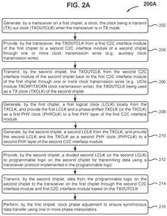
Low-latency aligned modules for data streams
PatentPendingUS20250111119A1
Innovation
- A system and method for low-latency data transfer between chiplets using a low-latency synchronous clock forwarded UCIe interface module that bypasses protocol and adapter layers, maintaining transceiver-generated clock characteristics, and includes alignment circuitry for flexible multi-module alignment.
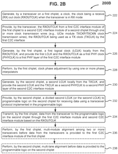
Low-latency aligned modules for data streams
PatentWO2025071864A1
Innovation
- The implementation of low-latency aligned data streams between chiplets through UCIe interface modules, which includes transmitting transceiver-generated clocks directly between chiplets, bypassing protocol layers, and using alignment circuitry for flexible module alignment.
Interoperability and Standardization Considerations
The UCIe (Universal Chiplet Interconnect Express) standard represents a pivotal development in chiplet-based system design, necessitating robust interoperability frameworks and standardization approaches. The consortium behind UCIe, including industry leaders such as Intel, AMD, ARM, and TSMC, has established comprehensive specifications to ensure seamless integration across different vendors' chiplets.
Interoperability within UCIe operates across multiple dimensions. At the physical layer, standardized die-to-die interfaces with defined electrical characteristics ensure signal integrity between chiplets regardless of manufacturer. The protocol layer standardization enables consistent communication methodologies, while the software layer provides uniform APIs for system-level integration.
The UCIe standard incorporates three critical protocol mapping methods to facilitate interoperability: Standard, Advanced, and Custom. The Standard mapping provides baseline compatibility for general-purpose applications, while Advanced mapping offers optimized performance for specific use cases. Custom mapping allows vendors to implement proprietary solutions while maintaining compliance with the broader UCIe framework.
Standardization efforts for UCIe have focused on creating a unified ecosystem while allowing sufficient flexibility for innovation. The specification defines mandatory compliance points alongside optional features, creating a tiered approach to certification. This balance between rigid standardization and flexibility has been crucial for industry adoption, allowing companies to differentiate their offerings while ensuring basic interoperability.
Testing and validation methodologies represent another critical aspect of UCIe standardization. The consortium has developed comprehensive compliance test suites covering electrical, logical, and protocol-level verification. These standardized testing procedures ensure that chiplets from different vendors can reliably communicate when integrated into a single package.
Future standardization roadmaps for UCIe include expanding protocol support beyond the current PCIe, CXL, and memory interfaces to encompass emerging interconnect technologies. Additionally, efforts are underway to harmonize UCIe with complementary standards such as ODSA and OCP, creating a more cohesive heterogeneous integration ecosystem.
The economic implications of UCIe standardization are substantial, potentially reducing development costs by enabling chiplet reuse across different products and manufacturers. This standardization also lowers barriers to entry for smaller companies, fostering innovation by allowing specialized chiplet development without the need to design entire SoCs.
Power and Thermal Management in UCIe Implementations
Power management in UCIe implementations represents a critical design consideration as chiplet-based architectures continue to evolve. The UCIe standard incorporates sophisticated power management capabilities across its protocol layers, enabling dynamic power optimization based on workload requirements. These capabilities include multiple power states that allow chiplets to transition between active, idle, and sleep modes with minimal latency, thereby conserving energy during periods of reduced activity.
Thermal management within UCIe implementations leverages both hardware and software approaches to maintain optimal operating temperatures. The standard defines thermal sensors and monitoring mechanisms that provide real-time temperature data across the chiplet ecosystem. This information feeds into thermal management algorithms that can dynamically adjust clock frequencies, voltage levels, and workload distribution to prevent hotspots and thermal throttling.
The die-to-die (D2D) interfaces in UCIe implementations incorporate power-efficient signaling techniques that significantly reduce energy consumption compared to traditional off-package interconnects. Advanced features such as link width modulation and frequency scaling allow for dynamic adaptation of interconnect bandwidth based on communication demands, further enhancing power efficiency.
UCIe's protocol layers implement power-aware flow control mechanisms that minimize unnecessary data transfers and buffer utilization. These mechanisms include credit-based flow control and quality of service features that prioritize critical transactions while allowing non-critical communications to be scheduled during periods of lower power consumption.
Thermal design considerations in UCIe implementations extend to package-level solutions, including advanced thermal interface materials and integrated heat spreaders optimized for multi-die packages. The standard supports coordinated thermal management across chiplets from different vendors, enabling system-level thermal optimization despite heterogeneous integration challenges.
Power delivery network (PDN) design represents another crucial aspect of UCIe implementations, with the standard supporting distributed power delivery architectures that minimize IR drop and ensure stable voltage across all chiplets. Advanced power gating techniques allow for selective deactivation of unused chiplet components, further reducing static power consumption in complex systems.
As UCIe adoption increases, emerging techniques such as AI-driven power management and predictive thermal modeling are being integrated into chiplet ecosystems, enabling more sophisticated approaches to balancing performance and energy efficiency in next-generation computing systems.
Unlock deeper insights with PatSnap Eureka Quick Research — get a full tech report to explore trends and direct your research. Try now!
Generate Your Research Report Instantly with AI Agent
Supercharge your innovation with PatSnap Eureka AI Agent Platform!