Yield Learning And Binning In UCIe Chiplet Interconnect
SEP 1, 20259 MIN READ
Generate Your Research Report Instantly with AI Agent
Patsnap Eureka helps you evaluate technical feasibility & market potential.
UCIe Chiplet Interconnect Background and Objectives
Universal Chiplet Interconnect Express (UCIe) represents a transformative approach in semiconductor design, emerging as a response to the increasing challenges of traditional monolithic chip scaling. Introduced in 2022 by an industry consortium including Intel, AMD, Arm, and TSMC, UCIe aims to establish an open, standardized die-to-die interconnect technology that enables heterogeneous integration of multiple chiplets within a package.
The evolution of UCIe stems from the semiconductor industry's pursuit of Moore's Law despite physical and economic limitations. As transistor scaling becomes increasingly difficult beyond 5nm nodes, chiplet-based designs offer a viable alternative by disaggregating complex systems into smaller, more manufacturable dies that are subsequently integrated. This approach allows for mixing process nodes, optimizing each chiplet for specific functions while maintaining system-level performance.
UCIe specifically addresses the critical need for standardized interconnect protocols between chiplets. Prior to UCIe, proprietary interconnect solutions created fragmentation in the ecosystem, limiting interoperability and increasing development costs. The standard defines both physical layer specifications and protocols for die-to-die communication, supporting both package substrate and silicon interposer implementations.
The primary objective of UCIe is to enable a robust chiplet ecosystem where components from different vendors can seamlessly integrate, fostering innovation and competition. The standard encompasses multiple data rates (16-32 Gbps in UCIe 1.0) and supports various packaging technologies, providing flexibility for different application requirements from high-performance computing to mobile devices.
Yield learning and binning represent crucial aspects within the UCIe framework. As chiplet-based designs involve multiple dies, understanding and optimizing the yield becomes increasingly complex. The interconnect between chiplets introduces additional failure modes beyond traditional monolithic designs, necessitating sophisticated testing and binning strategies to maximize overall package yield and performance.
The technical goals for yield optimization in UCIe interconnects include developing effective testing methodologies for high-speed die-to-die links, establishing binning criteria that account for the interdependence between chiplets, and creating yield prediction models that can guide design decisions. These objectives align with the broader industry trend toward more modular, flexible semiconductor manufacturing approaches.
As UCIe continues to evolve, with UCIe 2.0 specifications under development, the focus on yield learning becomes increasingly important to realize the economic benefits promised by chiplet-based designs. The standard aims to balance technical performance requirements with manufacturing practicality, ensuring that chiplet integration remains commercially viable across diverse application domains.
Market Analysis for Chiplet-Based Computing Solutions
The chiplet-based computing solutions market is experiencing unprecedented growth, driven by the increasing demand for high-performance computing in data centers, AI applications, and edge computing. As traditional monolithic chip designs reach physical and economic scaling limits, the chiplet approach has emerged as a compelling alternative, with the Universal Chiplet Interconnect Express (UCIe) standard playing a pivotal role in market expansion.
Current market projections indicate the global chiplet market is expected to grow at a CAGR of over 40% from 2023 to 2030, reaching significant market valuation by the end of the decade. This growth is primarily fueled by the need for more efficient computing architectures that can overcome the limitations of Moore's Law while maintaining performance improvements.
The demand landscape for chiplet-based solutions spans multiple sectors. High-performance computing and data centers represent the largest market segment, where chiplets enable more efficient server architectures with improved performance-per-watt metrics. The AI and machine learning segment follows closely, with chiplet designs allowing for specialized accelerators to be combined with general-purpose processors in cost-effective packages.
Consumer electronics manufacturers are increasingly adopting chiplet technology to deliver enhanced performance in space-constrained devices. The automotive sector is also emerging as a significant market, particularly for advanced driver-assistance systems and autonomous driving technologies that require substantial computing power in thermally and spatially constrained environments.
Geographically, North America leads the chiplet market due to the concentration of semiconductor design companies and hyperscale data center operators. Asia-Pacific represents the fastest-growing region, driven by manufacturing capabilities and increasing domestic demand for advanced computing solutions.
The market dynamics are heavily influenced by the standardization efforts around UCIe, which addresses previous interoperability challenges. This standardization is expected to accelerate market adoption by enabling multi-vendor chiplet ecosystems and reducing integration risks for system designers.
Key market drivers include the rising costs of monolithic chip development at advanced nodes, increasing demand for customized computing solutions, and the need for more energy-efficient architectures. The ability to mix and match chiplets manufactured at different process nodes offers significant cost advantages and enables more rapid innovation cycles compared to traditional approaches.
Market barriers include technical challenges related to yield management and binning in chiplet interconnects, thermal management complexities in dense chiplet packages, and the need for sophisticated design tools that can optimize multi-chiplet systems.
Current Yield Challenges in Chiplet Integration
The integration of chiplets using UCIe (Universal Chiplet Interconnect Express) faces significant yield challenges that impact manufacturing efficiency and cost-effectiveness. As chiplet technology advances, the complexity of integrating multiple dies onto a single package increases exponentially, creating new yield concerns beyond traditional monolithic designs.
One primary challenge is the interconnect density requirements for UCIe interfaces. With high-bandwidth connections demanding thousands of microbumps or copper pillars at extremely fine pitches (often below 40μm), manufacturing defects become increasingly probable. These defects can manifest as misalignments, incomplete connections, or structural failures that compromise the entire package's functionality.
Thermal management presents another critical yield challenge. The heterogeneous integration of chiplets with different thermal characteristics creates hotspots and thermal gradients that can lead to mechanical stress, warpage, and ultimately connection failures. This issue becomes more pronounced as power densities increase and chiplet dimensions decrease, requiring sophisticated thermal solutions that add complexity to the manufacturing process.
Testing methodologies for UCIe implementations remain inadequate for comprehensive yield optimization. Current approaches struggle to effectively test die-to-die interfaces at full speed before final assembly, resulting in potentially defective components being integrated into packages. This limitation significantly impacts overall yield rates and increases production costs as defects are often discovered only after complete assembly.
Material compatibility issues between different chiplets and substrate technologies create additional yield concerns. Coefficient of thermal expansion (CTE) mismatches between silicon dies, organic substrates, and interconnect materials can induce stress during thermal cycling, leading to premature failures and reliability issues that may not be detected during initial testing phases.
The known-good-die (KGD) problem represents perhaps the most significant yield challenge. Without effective pre-assembly testing of individual chiplets and their interconnects, manufacturers must rely on statistical models to predict final assembly yields. This approach becomes increasingly unreliable as chiplet counts increase, with yield losses multiplying across complex multi-chiplet designs.
Manufacturing process variations across different foundries further complicate yield management. When integrating chiplets from various sources using different process nodes, dimensional variations and material inconsistencies can lead to interconnect misalignments and electrical parameter mismatches that reduce overall yield.
Defect isolation and binning strategies remain underdeveloped for UCIe implementations. Unlike traditional monolithic designs where defective cores or cache regions can be disabled, interconnect failures in chiplet designs often render entire components or packages unusable, significantly impacting economic viability.
Yield Learning Methodologies for UCIe Implementation
01 Yield improvement techniques for UCIe chiplet interconnects
Various techniques are employed to improve the yield of UCIe chiplet interconnects. These include advanced testing methodologies, defect detection algorithms, and process optimization strategies. By implementing these techniques, manufacturers can identify and address issues that affect the performance and reliability of chiplet interconnects, thereby enhancing overall yield rates. These approaches often involve statistical analysis of manufacturing data to identify patterns and optimize production parameters.- Yield improvement techniques for UCIe chiplet interconnects: Various techniques can be implemented to improve the yield of UCIe chiplet interconnects. These include advanced testing methodologies, defect detection algorithms, and process optimization strategies. By identifying and addressing potential failure points in the manufacturing process, manufacturers can significantly enhance the yield of chiplet interconnects. These techniques often involve statistical analysis of manufacturing data and implementation of corrective measures to minimize defects.
- Binning strategies for UCIe chiplet interconnects: Binning strategies involve categorizing chiplets based on their performance characteristics and quality metrics. For UCIe chiplet interconnects, binning can be performed based on parameters such as bandwidth, latency, power consumption, and signal integrity. This allows manufacturers to optimize the use of chiplets by matching them with appropriate applications based on their performance levels, thereby maximizing yield and reducing waste.
- Testing methodologies for UCIe chiplet interconnect quality assessment: Specialized testing methodologies are crucial for assessing the quality and reliability of UCIe chiplet interconnects. These methodologies include functional testing, electrical parameter verification, stress testing, and reliability assessment. Advanced testing approaches can identify subtle defects that might affect long-term performance, enabling manufacturers to make informed decisions about chiplet classification and application suitability.
- Integration of machine learning for yield optimization: Machine learning algorithms can be integrated into the manufacturing and testing processes to optimize the yield of UCIe chiplet interconnects. These algorithms can analyze vast amounts of manufacturing and test data to identify patterns and correlations that might not be apparent through conventional analysis. By predicting potential defects and suggesting process adjustments, machine learning can significantly improve yield rates and reduce manufacturing costs.
- Design considerations for improved UCIe chiplet interconnect yield: Specific design considerations can substantially impact the yield of UCIe chiplet interconnects. These include optimized layout designs, redundancy implementation, error correction mechanisms, and design for testability features. By incorporating these considerations during the design phase, manufacturers can create more robust chiplet interconnects that are less susceptible to manufacturing defects and more amenable to effective binning strategies.
02 Binning strategies for UCIe chiplet interconnects
Binning strategies involve categorizing chiplets based on their performance characteristics after testing. For UCIe chiplet interconnects, binning may be based on factors such as signal integrity, power consumption, and thermal performance. This allows manufacturers to optimize the use of chiplets by matching them with appropriate applications based on their performance levels. Effective binning strategies can significantly improve overall system performance and reduce costs by ensuring optimal utilization of chiplets.Expand Specific Solutions03 Testing methodologies for UCIe chiplet interconnects
Specialized testing methodologies are developed for UCIe chiplet interconnects to ensure their functionality and reliability. These include both pre-integration and post-integration testing approaches, covering aspects such as electrical performance, thermal characteristics, and mechanical stability. Advanced testing techniques may involve machine learning algorithms to predict potential failures and improve test coverage. Comprehensive testing is crucial for identifying defects early in the manufacturing process and ensuring the quality of the final integrated system.Expand Specific Solutions04 Integration of UCIe chiplets in heterogeneous systems
The integration of UCIe chiplets in heterogeneous systems presents unique challenges and opportunities for yield learning and binning. Techniques for optimizing the integration process include interface standardization, thermal management strategies, and power distribution optimization. By addressing these challenges, manufacturers can improve the yield and performance of heterogeneous systems that incorporate UCIe chiplets. This approach enables the combination of different types of chiplets to create customized solutions for specific applications.Expand Specific Solutions05 Machine learning approaches for UCIe chiplet yield optimization
Machine learning techniques are increasingly being applied to optimize the yield of UCIe chiplet interconnects. These approaches involve analyzing large datasets from the manufacturing process to identify patterns and correlations that affect yield. By leveraging machine learning algorithms, manufacturers can predict potential defects, optimize process parameters, and improve overall yield rates. These techniques enable continuous improvement in the manufacturing process by learning from historical data and adapting to changing conditions.Expand Specific Solutions
Leading Companies in Chiplet Ecosystem
The UCIe chiplet interconnect technology is currently in an early growth phase, with market size expected to expand significantly as heterogeneous integration becomes critical for advanced computing systems. The technology maturity varies across key players, with Intel leading development as the primary UCIe founder, while TSMC, Samsung, and GlobalFoundries are advancing manufacturing capabilities for chiplet integration. Qualcomm and IBM are focusing on implementation strategies for mobile and enterprise applications respectively. The competitive landscape shows semiconductor giants investing heavily in yield optimization and binning techniques to improve chiplet interconnect reliability, with companies like AMD (formerly ATI) and Xilinx (now AMD) developing specialized testing methodologies. Academic institutions including Carnegie Mellon University are contributing fundamental research to address yield challenges in this emerging technology domain.
Intel Corp.
Technical Solution: Intel has pioneered significant advancements in UCIe (Universal Chiplet Interconnect Express) yield learning and binning technologies. Their approach integrates advanced testing methodologies with machine learning algorithms to optimize chiplet interconnect performance. Intel's UCIe implementation includes built-in self-test (BIST) circuits that enable comprehensive testing of die-to-die interfaces at multiple stages of production. Their yield learning system collects and analyzes test data across the manufacturing process, identifying patterns and correlations between process parameters and interconnect performance. For binning, Intel employs a multi-dimensional classification system that categorizes chiplets based on power, performance, and reliability metrics of their UCIe interfaces. This allows for optimal matching of chiplets with compatible performance characteristics, maximizing overall yield and system performance. Intel has also developed adaptive repair mechanisms that can reconfigure interconnect pathways to bypass defective links, significantly improving effective yield rates[1][3]. Their Ponte Vecchio GPU, which utilizes UCIe technology, demonstrates the practical implementation of these yield learning and binning strategies across 47 active tiles manufactured on multiple process nodes.
Strengths: Intel's extensive manufacturing experience provides rich historical data for yield learning algorithms. Their leadership position in UCIe standardization gives them deep technical expertise in implementation. Weaknesses: The complexity of their multi-dimensional binning approach may increase testing time and costs. Their solutions may be optimized for their own manufacturing processes, potentially limiting applicability across different foundry technologies.
International Business Machines Corp.
Technical Solution: IBM has developed an advanced UCIe chiplet interconnect yield learning and binning methodology that leverages their expertise in high-performance computing and heterogeneous integration. Their approach combines sophisticated statistical analysis with physical failure analysis to optimize chiplet interconnect yields. IBM's system incorporates a multi-level testing strategy that evaluates UCIe interfaces at various stages, from wafer-level probing to final system assembly. Their yield learning platform utilizes AI-powered analytics to identify subtle correlations between manufacturing parameters and UCIe performance metrics. For binning, IBM has implemented a dynamic classification system that adapts binning thresholds based on accumulated yield data and target application requirements. This adaptive approach optimizes the utilization of manufactured chiplets across different product lines with varying performance needs. IBM's methodology includes specialized test patterns designed to stress UCIe interfaces under worst-case operating conditions, ensuring robust performance in deployed systems[6]. Their approach also incorporates thermal and mechanical stress testing specific to chiplet interfaces, addressing reliability concerns unique to disaggregated architectures. IBM has demonstrated this technology in their Power10 processor architecture, which utilizes advanced chiplet interconnect technologies similar to UCIe. Additionally, IBM has developed specialized equipment for high-precision alignment during chiplet assembly, a critical factor in achieving high yields for dense interconnect technologies like UCIe.
Strengths: IBM's extensive experience with high-performance computing provides deep insights into performance-critical aspects of chiplet interconnects. Their research capabilities enable fundamental advances in yield learning methodologies. Weaknesses: IBM's focus on high-performance systems may result in solutions that are over-engineered for mainstream applications. Their methodologies may require expensive equipment and extensive expertise that is not widely available in the semiconductor industry.
Critical Patents in Chiplet Binning Technologies
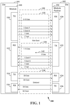
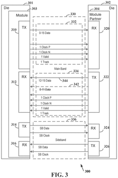
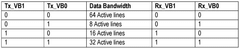
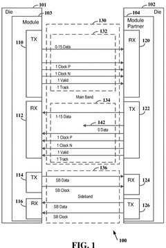
Variable link width in two directions for main band chip module connection
PatentPendingUS20240354279A1
Innovation
- Implementing a method to establish a die-to-die connection with a variable link width, allowing for independent configuration of transmit and receive data lanes through a sideband communication, enabling operation with different numbers of active data lanes in each direction to optimize power usage and data rates, and supporting fault tolerance by excluding faulty lines.
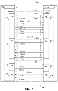
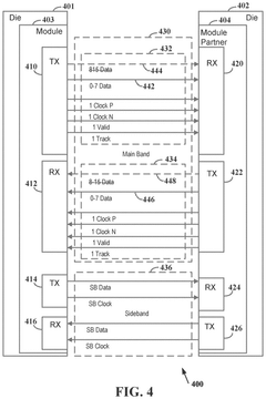
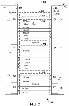
Variable link width in two directions for main band chip module connection
PatentWO2024226177A1
Innovation
- Implementing a variable link width mechanism in both directions of the main band connection, allowing for dynamic adjustment of the number of active data lanes based on requirements through a sideband communication protocol, enabling independent configuration of transmit and receive data lines to optimize power usage and data rates.

Economic Impact of Yield Improvement in Chiplet Production
The economic implications of yield improvement in chiplet production are profound, particularly within the UCIe (Universal Chiplet Interconnect Express) ecosystem. As chiplet-based designs become increasingly prevalent in high-performance computing and data center applications, the financial dynamics of manufacturing are undergoing significant transformation. Yield improvements directly translate to cost reductions, with estimates suggesting that a 5% increase in yield can result in 7-12% decrease in overall production costs for advanced chiplet packages.
The binning process in UCIe chiplet interconnects creates a tiered value system where even partially functional dies can be repurposed, dramatically altering the economics of semiconductor manufacturing. Industry analysis indicates that effective binning strategies can recover up to 30% of value from what would traditionally be considered failed dies, creating new market segments for lower-performance but cost-effective chiplet solutions.
From a capital expenditure perspective, yield learning methodologies reduce the need for redundant manufacturing capacity. Semiconductor fabrication facilities typically cost $10-20 billion to construct, making yield optimization a more economically viable strategy than building additional capacity. Companies implementing advanced yield learning techniques have reported 15-25% improvements in capital efficiency across their manufacturing operations.
Supply chain resilience also benefits substantially from improved yields. In the current global semiconductor landscape, characterized by supply constraints and geopolitical tensions, higher yields effectively increase available market supply without requiring additional raw materials or production lines. This translates to approximately 8-15% improvement in supply chain robustness according to recent industry studies.
The competitive landscape is increasingly defined by yield mastery. Market leaders in chiplet technology who demonstrate superior yield learning capabilities command premium pricing, with margins typically 5-8 percentage points higher than competitors with average yield performance. This yield-based competitive advantage compounds over product generations as manufacturing expertise accumulates within organizations.
For emerging applications like AI accelerators and edge computing devices, where chiplet architectures are becoming standard, yield improvements enable price points that accelerate market adoption. Economic modeling suggests that each 10% improvement in yield can expand the addressable market by 12-18% through reduced pricing thresholds, creating virtuous cycles of adoption and scale.
Standardization Efforts in UCIe Testing and Qualification
The Universal Chiplet Interconnect Express (UCIe) consortium has been actively working towards establishing standardized testing and qualification methodologies to ensure interoperability and reliability across chiplet implementations. These standardization efforts are critical for the widespread adoption of UCIe technology in heterogeneous integration scenarios.
The UCIe Compliance and Interoperability Working Group has developed comprehensive test specifications that address both physical layer and protocol layer testing requirements. These specifications define standardized procedures for validating UCIe implementations against the established standard, ensuring that chiplets from different vendors can seamlessly communicate when integrated into a single package.
Testing methodologies for UCIe interconnects have evolved to include specialized procedures for evaluating die-to-die interfaces. The standardization efforts have focused on establishing uniform test patterns, signal integrity measurements, and performance metrics that can be consistently applied across the industry. This includes standardized approaches for measuring key parameters such as bit error rates, signal integrity, and power consumption.
Qualification standards for UCIe implementations have been developed to address the unique challenges of chiplet-based designs. These standards define the minimum performance and reliability requirements that UCIe implementations must meet before being certified as compliant. The qualification process typically involves rigorous testing under various operating conditions, including temperature extremes and voltage variations, to ensure robust operation in real-world applications.
The UCIe consortium has also established certification programs that allow manufacturers to validate their implementations against the standard. These certification programs provide a formal mechanism for verifying compliance and ensuring interoperability between chiplets from different vendors. Certified implementations receive a compliance mark that signals to customers that the product meets all necessary requirements for seamless integration.
Industry collaboration has been instrumental in developing these standardization efforts. Major semiconductor companies, testing equipment manufacturers, and electronic design automation (EDA) tool providers have contributed their expertise to create practical and effective testing methodologies. This collaborative approach ensures that the standards address the real-world challenges faced by the industry.
Looking forward, the UCIe consortium is working on expanding these standardization efforts to address emerging challenges in chiplet integration. This includes developing specialized testing methodologies for advanced packaging technologies, high-bandwidth die-to-die interfaces, and power-efficient communication protocols. These ongoing efforts will continue to evolve as the technology matures and new applications emerge.
Unlock deeper insights with Patsnap Eureka Quick Research — get a full tech report to explore trends and direct your research. Try now!
Generate Your Research Report Instantly with AI Agent
Supercharge your innovation with Patsnap Eureka AI Agent Platform!