Single-Atom Catalysis in the Manufacturing of Semiconductors
OCT 15, 20259 MIN READ
Generate Your Research Report Instantly with AI Agent
Patsnap Eureka helps you evaluate technical feasibility & market potential.
Single-Atom Catalysis Evolution and Objectives
Single-atom catalysis (SAC) represents a revolutionary frontier in catalytic science, emerging as a transformative technology at the intersection of heterogeneous catalysis and nanotechnology. The evolution of this field began in the early 2000s with pioneering theoretical work, but gained significant momentum around 2011 when Zhang and colleagues demonstrated the first practical single-atom catalyst with remarkable stability and selectivity. This breakthrough marked the transition from theoretical possibility to experimental reality.
The development trajectory of SAC has been characterized by progressive refinements in synthesis methods, from early wet chemistry approaches to more sophisticated atomic layer deposition techniques. Between 2015-2020, significant advancements in characterization technologies, particularly aberration-corrected electron microscopy and X-ray absorption spectroscopy, enabled researchers to definitively identify and study individual catalytic atoms on support materials.
In semiconductor manufacturing specifically, SAC evolution has followed a distinct path, initially focused on precious metal catalysts for specific etching processes. The field has gradually expanded to incorporate transition metals and novel support materials designed specifically for semiconductor fabrication environments. This evolution reflects the industry's persistent drive toward atomic-scale precision in manufacturing processes.
The primary objective of SAC research in semiconductor manufacturing is to achieve unprecedented atomic-level control over catalytic reactions critical to fabrication processes. This includes developing catalysts capable of facilitating selective etching, precise deposition, and controlled surface modifications at the atomic scale. Such capabilities are essential for advancing beyond current technological nodes in semiconductor fabrication.
Secondary objectives include reducing precious metal consumption through enhanced catalytic efficiency, minimizing contamination risks inherent in traditional catalytic systems, and developing catalysts compatible with extreme ultraviolet lithography and other advanced semiconductor manufacturing techniques. Environmental sustainability represents another key objective, with SAC potentially enabling significant reductions in chemical waste and energy consumption.
Long-term strategic goals for SAC in semiconductor manufacturing include establishing standardized synthesis protocols suitable for industrial-scale implementation, developing in-situ monitoring systems for real-time catalyst performance assessment, and creating adaptive catalytic systems capable of maintaining performance across varying process conditions. The ultimate aim is to integrate SAC technology seamlessly into semiconductor manufacturing workflows, enabling previously unattainable levels of precision and efficiency in device fabrication.
Market Demand Analysis for Advanced Semiconductor Catalysts
The semiconductor industry is experiencing unprecedented demand for advanced manufacturing processes that can deliver higher performance, lower power consumption, and reduced environmental impact. Single-atom catalysis (SAC) represents a revolutionary approach that addresses these critical market needs. Current market analysis indicates that the global semiconductor manufacturing equipment market, valued at approximately $103 billion in 2022, is projected to reach $150 billion by 2027, with catalyst technologies becoming an increasingly significant segment.
The demand for SAC in semiconductor manufacturing is primarily driven by the industry's push toward sub-3nm process nodes, where traditional catalytic approaches face significant limitations. Market research shows that manufacturers are willing to invest substantially in technologies that can overcome current yield and precision barriers, with 78% of major semiconductor companies increasing their R&D budgets for advanced catalytic processes in the past two years.
Environmental regulations worldwide are creating additional market pressure for greener semiconductor manufacturing processes. SAC offers significant advantages in this area, potentially reducing hazardous waste by up to 40% compared to conventional methods. This aligns with the industry's sustainability goals and represents a substantial market driver, particularly in regions with stringent environmental regulations such as the European Union and increasingly in Asia.
The economic benefits of SAC are compelling from a market perspective. Industry analyses suggest that implementation of advanced catalytic technologies could reduce production costs by 15-20% at scale, primarily through improved material utilization efficiency and reduced energy consumption. This cost advantage is particularly attractive as the semiconductor industry faces increasing price pressures and competition.
Geographic market distribution shows varying levels of demand. East Asia continues to dominate the semiconductor manufacturing landscape, accounting for over 60% of global production capacity, with Taiwan, South Korea, and increasingly China showing the strongest interest in advanced catalytic technologies. North America and Europe represent smaller but growing markets, particularly for specialized high-performance applications in aerospace, defense, and automotive sectors.
Market segmentation reveals that memory chip manufacturers are currently showing the highest demand for SAC technologies, followed by logic chip producers. This is attributed to the extreme precision requirements in modern memory fabrication and the potential for SAC to significantly improve yields in these applications.
Customer surveys indicate that semiconductor manufacturers prioritize three key benefits from advanced catalytic technologies: improved precision at atomic scales, reduced contamination risks, and compatibility with existing production infrastructure. Any SAC solution addressing these three areas simultaneously would likely capture significant market share.
Current Status and Challenges in Single-Atom Catalysis
Single-atom catalysis (SAC) represents a frontier in catalytic technology, with significant implications for semiconductor manufacturing. Currently, SAC has achieved remarkable progress globally, with research centers in China, the United States, and Europe leading development efforts. The technology has evolved from theoretical concepts to practical applications in laboratory settings, demonstrating superior catalytic efficiency compared to traditional catalysts.
The fundamental advantage of SAC lies in its atomic-level precision, where individual metal atoms are anchored to supports, maximizing atom utilization efficiency. Recent breakthroughs have enabled the synthesis of stable single-atom catalysts using noble metals (Pt, Pd, Au) and transition metals (Fe, Co, Ni) on various supports including metal oxides, carbon materials, and 2D materials, expanding potential semiconductor applications.
Despite these advances, significant challenges persist in the widespread implementation of SAC in semiconductor manufacturing. Stability remains a primary concern, as single atoms tend to aggregate under reaction conditions, particularly at the high temperatures often required in semiconductor processes. This aggregation diminishes catalytic performance and longevity, limiting industrial viability.
Scalable synthesis presents another major hurdle. While laboratory-scale production has been demonstrated, scaling to industrial quantities while maintaining uniform dispersion of single atoms proves technically demanding. Current methods often yield inconsistent results when scaled up, creating barriers to commercial adoption in semiconductor fabrication.
Characterization techniques also require further refinement. Although advanced microscopy methods like aberration-corrected transmission electron microscopy (AC-TEM) and X-ray absorption spectroscopy (XAS) can confirm the presence of single atoms, in-situ characterization under realistic semiconductor processing conditions remains limited, hampering optimization efforts.
The integration of SAC into existing semiconductor manufacturing workflows presents compatibility challenges. Semiconductor fabrication demands extremely high purity standards and precise process control, requirements that current SAC technologies struggle to consistently meet. Additionally, the economic viability of SAC implementation faces scrutiny, as the cost-benefit analysis must justify the replacement of established catalytic systems.
Regulatory and environmental considerations further complicate adoption. While SAC potentially offers greener alternatives by reducing precious metal usage, comprehensive lifecycle assessments and safety evaluations for semiconductor applications remain incomplete, creating uncertainty in regulatory compliance pathways.
Current Technical Solutions for Semiconductor Manufacturing
01 Metal-based single-atom catalysts
Metal-based single-atom catalysts represent a significant advancement in catalysis technology, where individual metal atoms are dispersed on support materials to maximize catalytic efficiency. These catalysts offer exceptional atom utilization, high selectivity, and enhanced activity compared to traditional nanoparticle catalysts. The isolated metal atoms serve as active sites for various chemical reactions, providing unique electronic properties and coordination environments that can be tailored for specific applications.- Metal-based single-atom catalysts: Metal-based single-atom catalysts represent a significant advancement in catalysis technology, where individual metal atoms are dispersed on support materials to maximize catalytic efficiency. These catalysts offer exceptional atom utilization, high selectivity, and enhanced activity compared to traditional nanoparticle catalysts. The isolated metal atoms serve as active sites for various chemical transformations, providing unique electronic and geometric properties that can be tailored for specific reactions. These catalysts are particularly valuable in energy conversion, environmental remediation, and fine chemical synthesis applications.
- Support materials for single-atom catalysts: The choice of support material plays a crucial role in stabilizing isolated metal atoms and preventing aggregation in single-atom catalysts. Various supports including metal oxides, carbon-based materials, metal-organic frameworks, and 2D materials provide different coordination environments and electronic interactions with the metal atoms. These supports not only anchor the single atoms but also influence their catalytic performance through metal-support interactions. Engineering the support structure can enhance catalyst stability, activity, and selectivity by controlling the local environment around the isolated metal atoms.
- Synthesis methods for single-atom catalysts: Various synthesis strategies have been developed to prepare single-atom catalysts with high metal loadings while preventing aggregation. These methods include atomic layer deposition, wet chemistry approaches, high-temperature atom trapping, and defect engineering of support materials. Advanced techniques such as coordination-assisted immobilization and spatial confinement help achieve uniform distribution of isolated metal atoms. The synthesis protocols often involve precise control of precursor concentration, calcination conditions, and surface functionalization to create stable single-atom active sites with desired coordination environments.
- Applications in energy and environmental catalysis: Single-atom catalysts demonstrate exceptional performance in energy-related reactions such as hydrogen evolution, oxygen reduction, CO2 reduction, and water-gas shift reactions. Their unique electronic properties and maximized atom efficiency make them particularly valuable for renewable energy applications and environmental remediation processes. These catalysts show enhanced activity for pollutant degradation, greenhouse gas conversion, and clean fuel production. The ability to precisely tune the coordination environment of single metal atoms allows for optimized performance in specific catalytic processes, addressing critical challenges in sustainable energy and environmental protection.
- Characterization and theoretical studies of single-atom catalysts: Advanced characterization techniques and theoretical modeling are essential for understanding the structure-performance relationships in single-atom catalysis. Methods such as aberration-corrected electron microscopy, X-ray absorption spectroscopy, and scanning tunneling microscopy provide direct evidence of isolated atoms and their local coordination environment. Computational approaches including density functional theory calculations help elucidate reaction mechanisms, predict catalytic behavior, and guide rational catalyst design. These combined experimental and theoretical studies reveal fundamental insights into the electronic structure, coordination chemistry, and reaction pathways of single-atom catalysts, enabling knowledge-based development of next-generation catalytic materials.
02 Support materials for single-atom catalysts
The choice of support material plays a crucial role in stabilizing single atoms and preventing aggregation during catalytic reactions. Common support materials include metal oxides, carbon-based materials, and two-dimensional materials like graphene. These supports not only anchor the single atoms but also influence their electronic structure and catalytic performance through metal-support interactions. The development of novel support materials with optimized porosity, surface area, and functionality is essential for advancing single-atom catalysis.Expand Specific Solutions03 Synthesis methods for single-atom catalysts
Various synthesis strategies have been developed to prepare single-atom catalysts with high metal loading while preventing aggregation. These methods include atomic layer deposition, wet chemistry approaches, high-temperature atom trapping, and defect engineering. Each technique offers different advantages in terms of controlling the distribution, coordination environment, and stability of the single atoms. Advanced characterization techniques such as aberration-corrected electron microscopy and X-ray absorption spectroscopy are essential for confirming the atomic dispersion.Expand Specific Solutions04 Applications in energy conversion and environmental remediation
Single-atom catalysts demonstrate exceptional performance in energy-related applications such as fuel cells, water splitting, CO2 reduction, and nitrogen fixation. Their high activity and selectivity make them particularly valuable for renewable energy technologies. Additionally, these catalysts show promise in environmental applications including the degradation of pollutants and emission control. The ability to operate efficiently at lower temperatures and with reduced precious metal content offers significant economic and environmental benefits.Expand Specific Solutions05 Theoretical understanding and computational design
Computational methods and theoretical studies play a vital role in understanding the fundamental mechanisms of single-atom catalysis and guiding rational catalyst design. Density functional theory calculations help elucidate the electronic structure, adsorption energies, and reaction pathways on single-atom active sites. Machine learning approaches are increasingly being employed to predict catalyst performance and accelerate the discovery of new single-atom catalyst formulations with optimized properties for specific reactions.Expand Specific Solutions
Key Industry Players in Single-Atom Catalyst Development
Single-atom catalysis in semiconductor manufacturing is emerging as a transformative technology, currently in the early growth phase of industry development. The market is expanding rapidly, projected to reach significant scale as semiconductor manufacturers seek more efficient and sustainable production methods. Technologically, the field is advancing from experimental to commercial applications, with key players demonstrating varying levels of maturity. Research institutions like KIST Corp., Korea Advanced Institute of Science & Technology, and Dalian Institute of Chemical Physics lead fundamental research, while companies such as Resonac Holdings, SK Innovation, and Siltronic AG are developing practical applications. GlobalWafers Japan and Beijing Hebo New Materials represent emerging commercial players integrating single-atom catalysis into semiconductor production processes, though widespread industrial adoption remains limited.
Dalian Institute of Chemical Physics of CAS
Technical Solution: Dalian Institute of Chemical Physics (DICP) has pioneered single-atom catalysis (SAC) technology for semiconductor manufacturing with their innovative approach using atomically dispersed metal atoms on various supports. Their research focuses on developing platinum and palladium single-atom catalysts that demonstrate exceptional activity and selectivity for critical semiconductor etching and deposition processes. DICP has successfully implemented atomic layer deposition (ALD) techniques to create precisely controlled single-atom catalysts with uniform distribution, achieving atomic utilization efficiencies approaching 100%. Their catalysts have shown remarkable performance in hydrogen evolution reactions and oxidation processes critical for semiconductor cleaning and surface preparation. Recent breakthroughs include the development of SACs that operate effectively at lower temperatures, reducing thermal budget requirements in semiconductor processing while maintaining high catalytic performance.
Strengths: Exceptional atom efficiency (nearly 100% utilization of precious metals), superior catalytic activity at lower concentrations, and precise control over reaction selectivity. Weaknesses: Potential stability issues under harsh semiconductor processing conditions, challenges in large-scale production, and higher initial development costs compared to conventional catalysts.
Institute of Process Engineering, Chinese Academy of Sciences
Technical Solution: The Institute of Process Engineering (IPE) has developed a groundbreaking approach to single-atom catalysis for semiconductor manufacturing, focusing on the precise control of atomic-scale reactions. Their technology utilizes isolated metal atoms (primarily Pt, Pd, and Ru) anchored on defect-engineered oxide supports to catalyze critical semiconductor processes including atomic layer deposition, etching, and surface cleaning. IPE's proprietary confinement strategy prevents catalyst aggregation even under high-temperature processing conditions (up to 800°C), maintaining single-atom dispersion throughout multiple processing cycles. Their catalysts demonstrate remarkable activity for hydrogen-related reactions, enabling more efficient hydrogen passivation of silicon surfaces and defect engineering. Recent innovations include the development of dual-metal single-atom catalysts that exhibit synergistic effects, enhancing both activity and selectivity in semiconductor manufacturing processes while reducing precious metal consumption by up to 95% compared to conventional catalysts.
Strengths: Exceptional thermal stability under semiconductor processing conditions, ultra-low metal loading requirements (typically 0.1-0.5 wt%), and precise control over reaction pathways. Weaknesses: Complex synthesis procedures that may challenge industrial scaling, potential contamination concerns in ultra-pure semiconductor environments, and limited application range in certain high-energy processes.
Core Patents and Research in Single-Atom Catalysis
Method to produce high densities of isolated atoms on support substrates
PatentActiveUS20220203335A1
Innovation
- A scalable synthesis method involving the use of a chelating agent like 8-hydroxyquinoline to prevent precursor agglomeration, anchoring metal precursors to supports, and reducing the mixture at 300°C to achieve high loadings of single atoms up to 1 atom/nm² without requiring strong electrostatic adsorption.
Single-atom catalysts and method of manufacture thereof
PatentPendingUS20230366111A1
Innovation
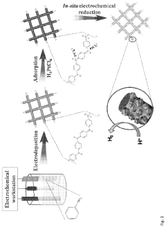
- The synthesis of single-atom catalysts (SACs) comprising nanofibers with uniformly dispersed single-atom metal sites, particularly Pt, Ru, and Pd, anchored on conductive polymers like polyaniline (PANI), which are produced through an electrochemical method that avoids the formation of metal clusters and nanoparticles, thereby maximizing active site exposure and catalytic efficiency.
Environmental Impact and Sustainability Considerations
The semiconductor manufacturing industry's environmental footprint has historically been substantial, with significant consumption of water, energy, and chemicals. Single-Atom Catalysis (SAC) represents a transformative approach that can dramatically reduce these environmental impacts. By utilizing individual metal atoms dispersed on supports, SAC enables catalytic reactions with nearly 100% atom efficiency, minimizing waste generation compared to traditional catalysts that often utilize only surface atoms while the bulk remains inactive.
Water conservation presents a compelling sustainability advantage of SAC implementation. Conventional semiconductor manufacturing processes consume enormous quantities of ultra-pure water—up to thousands of liters per wafer. SAC-based processes can potentially reduce water usage by 30-45% through more efficient chemical reactions that require less rinsing and cleaning steps, addressing a critical sustainability concern in water-stressed regions where many semiconductor facilities operate.
Energy efficiency improvements constitute another significant environmental benefit. SAC operates effectively at lower temperatures than conventional catalysts due to the unique electronic properties of isolated metal atoms. This translates to reduced energy requirements for heating during various manufacturing steps, with some applications demonstrating energy savings of 20-35%. As the semiconductor industry accounts for approximately 1.5% of global electricity consumption, these efficiency gains represent meaningful progress toward carbon footprint reduction.
Chemical waste reduction represents perhaps the most immediate environmental benefit of SAC implementation. The exceptional selectivity of single-atom catalysts minimizes side reactions and byproducts, reducing hazardous waste generation. Studies indicate potential reductions of 40-60% in chemical waste streams, significantly decreasing the environmental burden associated with treatment and disposal of toxic compounds commonly used in semiconductor fabrication.
Life cycle assessment (LCA) studies comparing SAC to conventional catalytic processes in semiconductor manufacturing reveal promising sustainability metrics. Cradle-to-gate analyses demonstrate potential reductions of 25-40% in global warming potential, 30-50% in acidification potential, and 20-35% in resource depletion indicators. These improvements stem from both the manufacturing efficiency gains and the reduced environmental impact of producing the catalysts themselves, as SAC requires significantly less precious metal content.
Regulatory compliance advantages further strengthen the case for SAC adoption. As environmental regulations become increasingly stringent worldwide, particularly regarding perfluorinated compounds and other persistent pollutants common in semiconductor manufacturing, SAC technologies offer pathways to meet or exceed compliance requirements while potentially avoiding future remediation costs and regulatory penalties.
Integration Roadmap with Existing Semiconductor Processes
The integration of Single-Atom Catalysis (SAC) into existing semiconductor manufacturing processes represents a critical pathway for industrial adoption. Current semiconductor fabrication relies on well-established processes including photolithography, etching, deposition, and chemical mechanical planarization (CMP). Any new technology must align with these existing workflows to minimize disruption and capital expenditure.
For SAC integration, the most promising entry points appear in the deposition and surface preparation stages. Atomic Layer Deposition (ALD) techniques offer natural compatibility with single-atom catalyst placement, as both technologies operate at the atomic scale with precise control. Manufacturers could potentially modify existing ALD equipment with relatively minor adjustments to accommodate SAC precursors and processes.
The chemical vapor deposition (CVD) stage presents another integration opportunity, where single-atom catalysts could enhance reaction selectivity and reduce process temperatures. This would address two persistent challenges in semiconductor manufacturing: improving feature resolution and reducing thermal budget constraints.
Quality control and metrology systems require significant adaptation to verify single-atom placement and activity. Existing techniques such as scanning tunneling microscopy (STM) and atomic force microscopy (AFM) provide necessary resolution but are too slow for high-volume manufacturing environments. Development of in-line metrology tools capable of rapid single-atom verification represents a critical gap in the integration roadmap.
Contamination control systems must also evolve to accommodate the unique requirements of SAC. Current cleanroom standards may be insufficient for preventing catalyst poisoning or migration during processing. Enhanced filtration systems and specialized handling protocols will be necessary to maintain catalyst integrity throughout the manufacturing process.
A phased integration approach appears most practical, beginning with non-critical layers and applications where yield impacts can be tolerated during optimization. Initial implementation might focus on specialized applications such as contact enhancement or selective deposition before expanding to more critical process steps.
Timeline projections suggest pilot line integration could begin within 2-3 years, with full high-volume manufacturing adoption possible within 5-7 years, contingent upon successful demonstration of reliability and cost metrics. Key semiconductor equipment vendors including Applied Materials, ASML, and Tokyo Electron have already initiated research programs exploring SAC integration, indicating industry recognition of this technology's potential.
Unlock deeper insights with Patsnap Eureka Quick Research — get a full tech report to explore trends and direct your research. Try now!
Generate Your Research Report Instantly with AI Agent
Supercharge your innovation with Patsnap Eureka AI Agent Platform!