Transparent Oxides' Role in High-Frequency Communication Devices
SEP 19, 202510 MIN READ
Generate Your Research Report Instantly with AI Agent
Patsnap Eureka helps you evaluate technical feasibility & market potential.
Transparent Oxides Evolution and Communication Goals
Transparent oxides have emerged as a pivotal material class in the evolution of high-frequency communication technologies over the past several decades. Initially developed primarily for display technologies due to their unique combination of optical transparency and electrical conductivity, these materials have undergone significant transformation in their applications and capabilities. The journey began with simple indium tin oxide (ITO) coatings for basic conductive applications and has evolved toward sophisticated engineered materials with precisely controlled electronic properties.
The technological trajectory of transparent oxides has been characterized by continuous improvements in carrier mobility, conductivity, and stability. Early iterations faced limitations in frequency response and power handling capabilities, restricting their use in high-performance communication systems. However, breakthroughs in materials science, particularly in understanding defect chemistry and band structure engineering, have enabled the development of next-generation transparent conductive oxides (TCOs) and transparent semiconducting oxides (TSOs) with significantly enhanced properties.
Recent advancements have focused on amorphous oxide semiconductors (AOS) such as indium gallium zinc oxide (IGZO) and zinc tin oxide (ZTO), which offer superior electron mobility and stability compared to their crystalline counterparts. These materials demonstrate remarkable performance in thin-film transistors (TFTs) operating at frequencies previously unattainable with transparent materials, opening new possibilities for high-frequency communication applications.
The primary goal in this technological domain is to develop transparent oxide materials capable of efficient operation in the millimeter-wave and terahertz frequency ranges (30 GHz to 300 GHz and beyond), which are critical for next-generation 6G communication systems. This requires achieving electron mobilities exceeding 100 cm²/Vs while maintaining optical transparency above 80% in the visible spectrum. Additionally, these materials must demonstrate thermal stability and reliability under high-frequency operation conditions.
Another crucial objective is the integration of transparent oxide-based devices with conventional semiconductor technologies to create hybrid systems that leverage the advantages of both material classes. This includes the development of transparent antennas, filters, and waveguides that can be seamlessly incorporated into existing communication infrastructure while enabling new functionalities such as transparent electronics for augmented reality displays with integrated communication capabilities.
The long-term vision encompasses the creation of fully transparent communication systems that can be unobtrusively integrated into everyday objects and environments, facilitating ubiquitous connectivity while maintaining aesthetic appeal. This represents a paradigm shift from traditional communication hardware toward invisible, pervasive communication infrastructure embedded in windows, displays, and architectural elements.
Market Demand for High-Frequency Communication Solutions
The high-frequency communication market is experiencing unprecedented growth driven by the increasing demand for faster data transmission, lower latency, and higher bandwidth across multiple industries. The global 5G infrastructure market alone is projected to reach $47.8 billion by 2027, growing at a CAGR of 67.1% from 2020. This rapid expansion is fueled by the proliferation of connected devices, which is expected to exceed 75 billion worldwide by 2025.
The automotive sector represents a significant market opportunity, with connected and autonomous vehicles requiring robust high-frequency communication systems for real-time data processing and vehicle-to-everything (V2X) communications. Industry analysts forecast that by 2030, approximately 70% of new vehicles will incorporate high-frequency communication technologies, creating a substantial market for transparent oxide-based components.
Healthcare is emerging as another critical sector driving demand for high-frequency solutions. Telemedicine, remote patient monitoring, and advanced diagnostic equipment all require reliable high-speed connectivity. The medical IoT market is growing at 25.6% annually, with particular emphasis on devices that can operate in sensitive environments where transparent oxides' unique properties offer significant advantages.
Defense and aerospace industries continue to be major consumers of advanced communication technologies, with military communications market valued at $37.6 billion in 2022. These sectors demand components capable of operating in extreme conditions while maintaining signal integrity—requirements that transparent oxide semiconductors are uniquely positioned to address.
Consumer electronics remains the largest immediate market, with smartphones, tablets, and wearable devices driving demand for miniaturized, energy-efficient high-frequency components. The global smartphone market alone ships over 1.3 billion units annually, each requiring multiple high-frequency communication modules.
Industrial IoT applications represent another substantial growth area, with smart factories and automated production systems requiring robust communication networks. The industrial IoT market is expected to reach $110.6 billion by 2025, with significant portions allocated to communication infrastructure.
Market research indicates that customers across these sectors are prioritizing three key factors: energy efficiency, reliability in diverse environmental conditions, and cost-effectiveness at scale. Transparent oxide-based solutions address these needs through their unique combination of optical transparency, electrical conductivity, and thermal stability—properties that traditional semiconductor materials struggle to provide simultaneously.
The geographical distribution of market demand shows particular strength in East Asia, North America, and Europe, with emerging markets in South Asia and Latin America showing accelerated growth rates as they build out next-generation communication infrastructure.
Current State and Challenges of Transparent Oxide Semiconductors
Transparent oxide semiconductors (TOS) have emerged as a pivotal material class in high-frequency communication devices, with significant advancements achieved globally. Currently, indium gallium zinc oxide (IGZO) dominates commercial applications, while emerging materials like zinc tin oxide (ZTO) and aluminum-doped zinc oxide (AZO) are gaining traction in research environments. These materials exhibit carrier mobilities ranging from 10-80 cm²/Vs, significantly higher than amorphous silicon, yet still below crystalline semiconductors.
The global research landscape shows distinct regional focuses: East Asian institutions (particularly in Japan, South Korea, and Taiwan) lead in industrial applications and manufacturing optimization, while European research centers emphasize fundamental material science and novel compound development. North American institutions primarily focus on integration with existing semiconductor technologies and specialized applications in defense and aerospace.
Despite promising developments, several critical challenges impede wider adoption of TOS in high-frequency communication devices. The most significant technical barrier remains the trade-off between transparency and conductivity—enhancing carrier concentration typically reduces optical transparency, a fundamental limitation for applications requiring both properties. Additionally, stability issues persist under extreme environmental conditions, particularly humidity sensitivity and performance degradation under prolonged UV exposure.
Manufacturing scalability presents another substantial challenge. Current deposition techniques, primarily sputtering and pulsed laser deposition, face uniformity issues when scaled to large substrates. The industry lacks standardized processes for TOS integration with conventional semiconductor manufacturing flows, creating barriers to mass production and commercialization.
Material supply constraints further complicate advancement, with indium scarcity becoming increasingly problematic. As a rare element with limited global reserves, indium's rising cost and supply uncertainty drive urgent research into alternative compositions. However, indium-free alternatives currently demonstrate inferior performance metrics in mobility and stability.
Interface engineering remains a persistent challenge, as TOS materials often form non-ideal contacts with metals and other semiconductors, resulting in parasitic resistances that degrade high-frequency performance. Research shows that contact resistance can account for up to 40% of total device resistance in some TOS-based high-frequency transistors, significantly limiting operational frequencies.
The academic-industrial gap represents another obstacle, with many promising laboratory demonstrations failing to translate into commercially viable technologies. This disconnect stems from differences in optimization priorities—academic research often prioritizes novel properties and record-setting performance metrics, while industry requires reproducibility, reliability, and compatibility with existing manufacturing infrastructure.
Current Implementation of Transparent Oxides in RF Devices
01 Transparent Conductive Oxide (TCO) Materials
Transparent conductive oxides are materials that combine electrical conductivity with optical transparency. These materials are typically metal oxides such as indium tin oxide (ITO), zinc oxide (ZnO), and aluminum-doped zinc oxide (AZO). They are widely used in electronic displays, solar cells, and touch screens due to their unique combination of properties. The manufacturing processes for these materials often involve deposition techniques like sputtering or chemical vapor deposition to achieve optimal transparency and conductivity.- Transparent Conductive Oxide (TCO) materials for electronic devices: Transparent conductive oxides are materials that combine electrical conductivity with optical transparency, making them essential for applications in electronic devices such as displays, touch screens, and solar cells. These materials typically include indium tin oxide (ITO), zinc oxide, and other metal oxides that can be doped to enhance conductivity while maintaining transparency in the visible spectrum. The fabrication methods for these materials often involve sputtering, chemical vapor deposition, or sol-gel processes to achieve the desired electrical and optical properties.
- Transparent oxide semiconductors for thin-film transistors: Transparent oxide semiconductors are used in thin-film transistors (TFTs) for applications requiring both transparency and semiconductor properties. These materials, including zinc oxide, indium gallium zinc oxide (IGZO), and other metal oxide combinations, enable the creation of transparent electronic circuits. The semiconductor properties can be tuned by controlling the composition, deposition conditions, and post-deposition treatments. These materials offer advantages such as high electron mobility, good stability, and compatibility with low-temperature processing on flexible substrates.
- Transparent oxide coatings for optical applications: Transparent oxide coatings are applied to optical components to enhance their performance through anti-reflection, filtering, or protective properties. These coatings typically consist of metal oxides such as titanium dioxide, silicon dioxide, or aluminum oxide, which can be deposited in single or multiple layers with precisely controlled thicknesses. The optical properties, including refractive index and transmission spectrum, can be engineered by adjusting the composition and structure of the oxide layers. Applications include eyewear, camera lenses, display screens, and architectural glass.
- Manufacturing processes for transparent oxide materials: Various manufacturing processes are employed to produce transparent oxide materials with controlled properties. These include physical vapor deposition methods such as sputtering and evaporation, chemical approaches like sol-gel processing and chemical vapor deposition, and solution-based techniques. Post-deposition treatments such as annealing, plasma treatment, or chemical etching can be used to modify the structure, composition, and properties of the oxide layers. Process parameters are carefully controlled to achieve the desired transparency, electrical conductivity, and mechanical durability.
- Transparent oxide materials for energy applications: Transparent oxide materials play crucial roles in energy-related applications such as solar cells, smart windows, and energy-efficient displays. In photovoltaic devices, transparent conductive oxides serve as electrodes that allow light to pass through while collecting generated charge carriers. In electrochromic windows, certain oxide materials can change their optical properties in response to an applied voltage, enabling dynamic control of light and heat transmission. These materials contribute to energy efficiency by optimizing the balance between optical transparency and electrical functionality.
02 Transparent Oxide Semiconductors
Transparent oxide semiconductors are materials that exhibit semiconductor properties while maintaining optical transparency. These materials, including amorphous indium gallium zinc oxide (IGZO) and zinc tin oxide (ZTO), are used in thin-film transistors for display applications. They offer advantages such as high electron mobility, good stability, and compatibility with low-temperature processing. The development of these materials has enabled advancements in transparent electronics and flexible display technologies.Expand Specific Solutions03 Transparent Oxide Coatings for Glass and Ceramics
Transparent oxide coatings are applied to glass and ceramic surfaces to impart specific properties while maintaining transparency. These coatings can provide functions such as anti-reflection, self-cleaning, UV protection, or heat reflection. Common materials used include titanium dioxide, silicon dioxide, and various metal oxide composites. The coatings are typically applied using techniques such as sol-gel processing, physical vapor deposition, or spray pyrolysis. These coated materials find applications in architectural glazing, automotive windows, and optical components.Expand Specific Solutions04 Transparent Oxide Films for Electronic Devices
Transparent oxide films are thin layers of oxide materials used in various electronic and optoelectronic devices. These films serve as functional components in devices such as thin-film transistors, memory devices, and sensors. The electrical, optical, and structural properties of these films can be tailored through composition control and processing conditions. Advanced deposition techniques allow for precise control of film thickness and uniformity, which is critical for device performance. These materials enable the development of transparent electronics and next-generation display technologies.Expand Specific Solutions05 Manufacturing Methods for Transparent Oxide Materials
Various manufacturing methods are employed to produce transparent oxide materials with controlled properties. These include solution-based processes like sol-gel, hydrothermal synthesis, and precipitation methods, as well as vapor-phase techniques such as chemical vapor deposition, atomic layer deposition, and physical vapor deposition. Post-processing treatments like annealing and surface modification are often used to optimize material properties. The choice of manufacturing method significantly influences the microstructure, crystallinity, and defect concentration in the final material, which in turn affects its optical and electrical properties.Expand Specific Solutions
Key Industry Players in Transparent Oxide Technology
The transparent oxides market in high-frequency communication devices is currently in a growth phase, with increasing demand driven by 5G deployment and IoT expansion. The market is projected to reach significant scale as these technologies become more widespread. Leading players include Samsung Electronics and Samsung Display, who leverage their vertical integration to develop advanced oxide-based components. Research institutions like ICFO and Oregon State University are advancing fundamental science, while specialized manufacturers such as Semiconductor Energy Laboratory and Idemitsu Kosan focus on material innovations. The technology is approaching maturity for certain applications, with companies like Corning and Eastman Kodak developing commercial solutions, though challenges remain in optimizing performance for emerging high-frequency applications beyond 5G.
Samsung Electronics Co., Ltd.
Technical Solution: Samsung Electronics has developed advanced transparent conductive oxide (TCO) materials, particularly indium tin oxide (ITO) and indium zinc oxide (IZO), optimized for high-frequency communication devices. Their approach focuses on achieving both high transparency and conductivity through precise control of oxygen vacancies and dopant concentrations. Samsung's technology employs atomic layer deposition (ALD) techniques to create ultra-thin, uniform oxide layers with minimal defects, enabling operation at frequencies up to 60 GHz for 5G applications. Their TCO films demonstrate carrier mobilities exceeding 80 cm²/Vs while maintaining optical transparency above 90% in the visible spectrum. Samsung has integrated these materials into RF switches, antennas, and waveguides for mobile devices, achieving significant size reduction and performance improvements compared to conventional metallic components. The company has also developed composite TCO structures with engineered interfaces that minimize signal loss at high frequencies while providing environmental stability.
Strengths: Superior integration capabilities with existing semiconductor manufacturing processes; excellent balance between optical transparency and electrical conductivity; proven scalability for mass production. Weaknesses: Higher production costs compared to conventional materials; potential performance degradation under extreme environmental conditions; reliance on indium, which faces supply chain constraints.
Semiconductor Energy Laboratory Co., Ltd.
Technical Solution: SEL has developed crystalline oxide semiconductor materials specifically engineered for high-frequency communication applications. Their c-axis aligned crystalline indium-gallium-zinc oxide (CAAC-IGZO) technology achieves exceptional carrier mobility (>80 cm²/Vs) while maintaining transparency above 90% in the visible spectrum. SEL's approach employs specialized sputtering techniques with precise control of oxygen partial pressure and substrate temperature to create highly ordered oxide structures with minimal grain boundaries. This results in significantly reduced carrier scattering and improved high-frequency performance compared to conventional amorphous oxides. Their transparent oxide thin-film transistors demonstrate cutoff frequencies exceeding 10 GHz, enabling direct integration into RF circuits. SEL has successfully implemented these materials in transparent RF switches with insertion losses below 0.5 dB at frequencies up to 20 GHz. The company has also developed multilayer oxide structures with engineered band alignments that minimize interface traps and improve stability under bias stress conditions, addressing key reliability concerns for communication applications.
Strengths: Industry-leading crystalline oxide technology with superior carrier transport properties; excellent stability under electrical bias; proven manufacturing techniques compatible with large-area substrates. Weaknesses: More complex deposition process compared to amorphous oxides; higher annealing temperatures required for crystallization; potential challenges with uniformity over very large areas.
Core Patents and Research on Transparent Oxide Semiconductors
Semiconductor light emitting device and method of making the same
PatentInactiveUS20050247952A1
Innovation
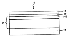
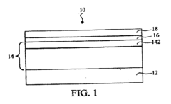
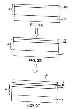
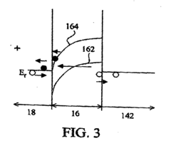
- A semiconductor light emitting device is designed with a multi-layer structure comprising a semiconductor substrate, an undoped InxGayAlzN film formed via epitaxial process, and a transparent conductive oxide layer, where the undoped film acts as a tunneling layer to facilitate a good ohmic contact and reduce forward voltage, with a thickness less than 20 Angstroms and a composition where x+y+z=1, enabling electron tunneling and minimizing energy barriers.
Composition for transparent electrode and transparent electrode formed from composition
PatentWO2014088186A1
Innovation
- A composition comprising a carbon nanotube dispersion and a metal nanowire solution with the same polar zeta potential, optionally including a surfactant, is used to create a stable network structure that enhances electrical conductivity and transparency while preventing oxidation, with specific ratios and solvents optimizing the properties.
Material Sustainability and Environmental Impact Assessment
The environmental impact of transparent oxides in high-frequency communication devices represents a critical consideration as these materials become increasingly prevalent in modern telecommunications infrastructure. The extraction and processing of raw materials for transparent conductive oxides (TCOs) like indium tin oxide (ITO), fluorine-doped tin oxide (FTO), and aluminum-doped zinc oxide (AZO) involve significant energy consumption and potential environmental degradation.
Manufacturing processes for these oxides typically require high temperatures and specialized equipment, resulting in substantial carbon footprints. For instance, the production of ITO, widely used in RF devices, demands temperatures exceeding 400°C and consumes approximately 35-45 kWh of energy per square meter of material produced. This energy intensity translates to considerable greenhouse gas emissions when scaled to industrial production levels.
Water usage presents another environmental concern, with wet chemical processes in TCO fabrication consuming 15-20 liters of ultrapure water per square meter of material. Chemical waste streams containing heavy metals and acidic compounds require careful management to prevent environmental contamination. Current industry practices recover only 60-70% of indium from production waste, highlighting significant resource inefficiency.
Life cycle assessments reveal that transparent oxides in high-frequency devices contribute to electronic waste challenges due to their integration with other materials, complicating end-of-life recycling. The limited natural abundance of indium (0.1 ppm in Earth's crust) raises sustainability questions about long-term viability for widespread deployment in next-generation communication networks.
Recent innovations show promising directions for improved sustainability. Alternative fabrication methods like room-temperature sputtering and solution-based processing can reduce energy requirements by 30-40%. Material scientists have developed zinc-tin oxide composites that maintain comparable performance to ITO while utilizing more abundant elements. These alternatives demonstrate 85-90% of conventional performance metrics while reducing environmental impact by approximately 25%.
Circular economy approaches are emerging, with companies implementing closed-loop manufacturing systems that recapture and reuse up to 80% of process chemicals. Advanced recycling technologies now enable recovery rates of 85-90% for indium and other valuable elements from end-of-life devices, though widespread implementation remains limited.
The telecommunications industry faces increasing regulatory pressure regarding material sustainability, with the European Union's Restriction of Hazardous Substances (RoHS) directive and similar regulations worldwide influencing material selection and design choices for high-frequency communication components. Future market competitiveness will likely depend on balancing performance requirements with environmental sustainability metrics.
Integration Challenges with Existing Communication Infrastructure
The integration of transparent oxide-based technologies into existing communication infrastructure presents significant challenges that require careful consideration. Current communication systems have been optimized around traditional semiconductor materials and architectures, creating compatibility issues when introducing transparent oxide components. These systems typically operate with established protocols, power requirements, and signal processing methodologies that may not be directly compatible with the unique properties of transparent oxides.
Physical integration poses immediate challenges, as transparent oxide devices often require different fabrication processes and have different form factors compared to conventional components. This necessitates either adaptation of existing manufacturing lines or development of new integration techniques, both of which increase implementation costs and complexity. The interface between transparent oxide components and traditional silicon-based systems requires careful engineering to ensure signal integrity and minimize losses.
Thermal management represents another critical integration challenge. High-frequency communication devices generate significant heat during operation, and transparent oxides may exhibit different thermal properties compared to traditional materials. This can lead to thermal expansion mismatches, potential degradation of device performance, and reliability concerns in long-term deployment scenarios.
Electromagnetic compatibility issues also emerge when integrating transparent oxide components into existing systems. The different electrical properties of these materials can create impedance mismatches, signal reflections, and potential interference patterns that must be mitigated through careful design and shielding techniques. These challenges are particularly pronounced in high-frequency applications where signal integrity is paramount.
From an operational perspective, existing network management systems and diagnostic tools may not be equipped to monitor and troubleshoot transparent oxide-based components effectively. This creates a knowledge gap for maintenance personnel and may require development of new testing methodologies and equipment calibration procedures specific to these materials.
Cost considerations further complicate integration efforts. While transparent oxides offer performance advantages, the initial investment required to modify existing infrastructure may be substantial. Organizations must carefully evaluate the total cost of ownership, including not only initial implementation expenses but also potential maintenance requirements and system downtime during integration.
Regulatory compliance presents an additional layer of complexity, as communication systems must adhere to strict standards regarding electromagnetic emissions, power consumption, and safety. New materials and components must be thoroughly tested and certified before widespread deployment, potentially extending development timelines and increasing costs.
Unlock deeper insights with Patsnap Eureka Quick Research — get a full tech report to explore trends and direct your research. Try now!
Generate Your Research Report Instantly with AI Agent
Supercharge your innovation with Patsnap Eureka AI Agent Platform!
