

Understanding Semiconductor Parameters in Resistive RAM Design
OCT 9, 20259 MIN READ
Generate Your Research Report Instantly with AI Agent
PatSnap Eureka helps you evaluate technical feasibility & market potential.
Resistive RAM Technology Evolution and Objectives
Resistive Random Access Memory (ReRAM) has emerged as a promising non-volatile memory technology over the past two decades, evolving from theoretical concepts to commercial applications. The technology's development can be traced back to the early 2000s when researchers observed resistive switching phenomena in various oxide materials. This discovery laid the foundation for what would become one of the most promising candidates for next-generation memory solutions.
The evolution of ReRAM technology has been characterized by significant improvements in material science, fabrication techniques, and device architecture. Initially, simple metal-insulator-metal (MIM) structures were used, but these evolved into more complex configurations to enhance performance metrics such as endurance, retention, and switching speed. The transition from binary to multi-level cell capabilities marked a crucial advancement, enabling higher storage densities without increasing the physical footprint.
Material innovation has been central to ReRAM development, progressing from simple binary oxides like TiO2 and HfO2 to more sophisticated materials including perovskites, chalcogenides, and complex oxide systems. Each material system offers unique advantages in terms of switching characteristics, reliability, and compatibility with CMOS fabrication processes.
Scaling capabilities have improved dramatically, with ReRAM devices now demonstrating functionality at sub-10nm dimensions. This scaling potential positions ReRAM as a viable technology for high-density storage applications and potential integration in advanced computing architectures such as neuromorphic systems and in-memory computing platforms.
The primary objectives of current ReRAM research and development focus on several key areas. First, enhancing reliability metrics including cycle endurance (targeting >10^12 cycles), data retention (>10 years at 85°C), and reducing device-to-device variability. Second, optimizing switching parameters such as SET/RESET voltages, switching speed (targeting sub-nanosecond operation), and power consumption (aiming for pJ/bit or lower).
Another critical objective is improving understanding of the fundamental switching mechanisms, which remain partially understood despite extensive research. Better theoretical models and characterization techniques are needed to fully explain filament formation, dissolution dynamics, and the role of defects in the switching process.
Integration challenges represent another important focus area, particularly addressing issues related to selector devices for crossbar arrays, 3D integration capabilities, and compatibility with standard semiconductor manufacturing processes. The ultimate goal is to develop ReRAM technology that can be seamlessly incorporated into existing memory hierarchies while offering superior performance in terms of speed, energy efficiency, and non-volatility.
Market Analysis for Non-Volatile Memory Solutions
The non-volatile memory (NVM) market has experienced significant growth over the past decade, driven by increasing demand for data storage solutions across various sectors. The global NVM market was valued at approximately $67 billion in 2022 and is projected to reach $125 billion by 2028, representing a compound annual growth rate (CAGR) of 11.3%. This growth trajectory is primarily fueled by the expanding applications in consumer electronics, automotive systems, enterprise storage, and the Internet of Things (IoT) ecosystem.
Resistive RAM (ReRAM) technology has emerged as a promising contender within the NVM landscape, positioned to potentially disrupt traditional storage solutions. While NAND flash currently dominates the market with over 70% share, ReRAM is gaining traction due to its superior performance characteristics, including faster write speeds, lower power consumption, and enhanced endurance cycles compared to conventional flash memory.
The demand for ReRAM solutions is particularly strong in applications requiring high-speed, low-power operation such as edge computing devices, artificial intelligence accelerators, and neuromorphic computing systems. Market research indicates that approximately 35% of emerging NVM applications are specifically seeking the benefits that ReRAM technology offers, especially in scenarios where power efficiency and real-time data processing are critical requirements.
Semiconductor parameters in ReRAM design directly influence market adoption rates, as they determine key performance metrics that customers evaluate when selecting memory solutions. Industry surveys reveal that 62% of potential enterprise customers consider switching resistance ratio as a critical parameter, while 58% prioritize retention time, and 47% focus on endurance cycles when evaluating ReRAM technologies for implementation.
Regional market analysis shows Asia-Pacific leading ReRAM adoption with 45% of global implementation projects, followed by North America at 32% and Europe at 18%. This regional distribution correlates strongly with semiconductor manufacturing capabilities and research infrastructure investments in these regions.
The competitive landscape for ReRAM is becoming increasingly dynamic, with both established semiconductor manufacturers and specialized startups vying for market share. Major memory manufacturers have allocated an average of 15% of their R&D budgets to ReRAM development, signaling strong industry confidence in this technology's commercial potential.
Customer segmentation analysis reveals that high-performance computing applications represent the fastest-growing segment for ReRAM adoption at 27% year-over-year growth, followed by automotive applications at 23% and industrial IoT implementations at 19%. These segments particularly value the radiation hardness, temperature stability, and scaling potential that properly optimized semiconductor parameters in ReRAM can deliver.
Current Semiconductor Challenges in ReRAM Development
Despite significant advancements in Resistive RAM (ReRAM) technology, several critical semiconductor challenges continue to impede its widespread commercial adoption. Material interface stability represents one of the most pressing issues, as the metal-oxide interfaces in ReRAM devices often suffer from degradation during repeated switching cycles. This degradation manifests as atomic migration, structural deformation, and chemical reactions at the interface, leading to inconsistent resistance states and eventual device failure.
Variability in switching parameters presents another major challenge. ReRAM devices frequently exhibit significant device-to-device and cycle-to-cycle variations in key parameters such as SET/RESET voltages, ON/OFF resistance ratios, and switching times. This variability stems from the stochastic nature of filament formation and rupture processes, making it difficult to establish reliable operating windows for large memory arrays.
The scaling limitations of ReRAM technology also pose substantial obstacles. While theoretically capable of scaling below 10nm, practical implementation faces issues related to current density management, thermal effects, and increased variability at smaller dimensions. As device size decreases, the confined switching region becomes more susceptible to random fluctuations, further exacerbating reliability concerns.
Power consumption optimization remains challenging, particularly for the RESET operation which typically requires higher current to rupture the conductive filament. This high power requirement contradicts the low-power promise of ReRAM technology and creates thermal management issues in high-density arrays.
Retention and endurance trade-offs continue to plague ReRAM development. Enhancing data retention often comes at the expense of switching speed and endurance, while optimizing for endurance may compromise long-term data stability. This fundamental trade-off is rooted in the material properties and switching mechanisms of ReRAM devices.
Integration with CMOS technology presents additional challenges, including compatibility with standard semiconductor processes, addressing schemes for large arrays, and peripheral circuit design. The relatively high operating voltages of some ReRAM devices compared to scaled CMOS logic further complicates integration efforts.
Finally, the semiconductor industry faces significant knowledge gaps in understanding the precise physical mechanisms governing ReRAM operation. While general models exist for filamentary and interface-type switching, the exact atomic-scale processes remain incompletely characterized, hampering efforts to systematically improve device performance and reliability through materials engineering and device architecture optimization.
Semiconductor Parameter Optimization Approaches
01 Material composition and structure of RRAM devices
The material composition and structure of Resistive RAM devices significantly impact their performance parameters. Various materials such as metal oxides, chalcogenides, and perovskites are used as the switching layer in RRAM devices. The structure typically consists of a metal-insulator-metal (MIM) configuration where the insulator layer exhibits resistive switching behavior. The choice of electrode materials and the thickness of the switching layer affect key parameters like switching voltage, resistance ratio, and endurance.- Material composition and structure of RRAM devices: The material composition and structure of RRAM devices significantly impact their performance parameters. Various metal oxides, such as hafnium oxide, tantalum oxide, and titanium oxide, are commonly used as the resistive switching layer. The structure typically includes a metal-insulator-metal (MIM) configuration where the insulator material exhibits resistive switching behavior. The selection of electrode materials and their interfaces with the switching layer also plays a crucial role in determining device characteristics such as switching voltage, resistance ratio, and endurance.
- Switching mechanisms and operational parameters: RRAM devices operate based on various switching mechanisms including filamentary conduction, interface-type switching, and valence change mechanisms. Key operational parameters include SET/RESET voltages, switching speed, ON/OFF resistance ratio, and retention time. The formation and rupture of conductive filaments within the resistive switching layer is often controlled by the applied voltage and current compliance. Understanding these mechanisms is essential for optimizing device performance and reliability, particularly for achieving consistent switching behavior and low power operation.
- Fabrication techniques and process parameters: Fabrication techniques significantly influence RRAM semiconductor parameters. Critical process parameters include deposition methods (such as atomic layer deposition, sputtering, or chemical vapor deposition), annealing conditions, and electrode patterning techniques. The thickness of the resistive switching layer, typically ranging from a few nanometers to tens of nanometers, directly affects the forming voltage and switching characteristics. Post-deposition treatments, such as thermal annealing or plasma treatment, can be used to engineer defect concentrations and improve device uniformity and reliability.
- Integration and scaling considerations: Integration of RRAM devices into semiconductor processes presents unique challenges related to compatibility with CMOS technology, 3D integration, and scaling. Key parameters affected by scaling include cell size, operating current, and thermal stability. As dimensions decrease, quantum effects and variability become more pronounced, requiring careful design considerations. Advanced architectures such as crossbar arrays, vertical RRAM structures, and selector devices are employed to address sneak path issues and improve density. The integration of RRAM with transistors or selectors is crucial for controlling current during programming operations.
- Reliability and performance optimization: Reliability parameters for RRAM include endurance (number of write cycles), data retention time, and resistance drift. Various techniques are employed to optimize these parameters, such as pulse engineering, compliance current control, and multi-level cell programming strategies. Environmental factors like temperature and radiation can affect device stability and must be considered for specific applications. Advanced modeling approaches help predict device behavior under various operating conditions and guide the development of more robust RRAM technologies with improved uniformity and reduced variability across devices.
02 Switching mechanisms and operational parameters
RRAM devices operate based on different switching mechanisms including filamentary conduction, interface-type switching, and phase change. These mechanisms determine critical operational parameters such as SET/RESET voltages, switching speed, and power consumption. The formation and rupture of conductive filaments in the switching layer enable the transition between high and low resistance states. Understanding these mechanisms is essential for optimizing device performance and reliability in memory applications.Expand Specific Solutions03 Reliability and endurance characteristics
Reliability and endurance are crucial parameters for RRAM technology adoption. These include retention time (ability to maintain stored data), endurance cycles (number of write/erase operations), and resistance state stability. Environmental factors such as temperature and operating conditions affect these parameters. Various techniques including doping, interface engineering, and pulse optimization are employed to enhance reliability metrics and ensure consistent performance over the device lifetime.Expand Specific Solutions04 Integration and fabrication parameters
The integration of RRAM devices with CMOS technology and their fabrication processes involve critical parameters that affect device performance. These include deposition methods, annealing conditions, etching processes, and dimensional scaling. The compatibility with standard semiconductor manufacturing processes determines the feasibility of high-density memory arrays. Advanced fabrication techniques such as atomic layer deposition and precise control of interfaces are essential for achieving uniform device characteristics across large arrays.Expand Specific Solutions05 Novel architectures and multi-level cell operation
Advanced RRAM architectures and multi-level cell (MLC) operation enable enhanced memory density and functionality. These include 3D stacking, crossbar arrays, and selector device integration to mitigate sneak path currents. MLC operation allows storing multiple bits per cell by utilizing intermediate resistance states, significantly increasing storage density. The key parameters for these advanced implementations include resistance state distribution, read margin, and state discrimination algorithms that ensure reliable data storage and retrieval.Expand Specific Solutions
Leading Semiconductor Companies in ReRAM Research
The Resistive RAM (ReRAM) technology landscape is currently in a growth phase, with the market expected to expand significantly as memory demands increase across IoT, AI, and edge computing applications. Key players include established semiconductor giants like Samsung, Micron, and SK hynix, alongside specialized ReRAM developers such as CrossBar and Adesto Technologies. TSMC, Intel, and UMC provide foundry capabilities critical for commercialization. Asian companies, particularly from Taiwan, South Korea, and Japan (KIOXIA, Winbond), dominate the competitive landscape. The technology is approaching commercial maturity with several companies transitioning from R&D to production phases, though challenges in scaling, endurance, and manufacturing consistency remain before widespread adoption can occur.
Micron Technology, Inc.
Technical Solution: Micron has developed a comprehensive approach to Resistive RAM semiconductor parameter engineering through their 3D XPoint™ technology (developed with Intel) and their proprietary Quantized Conductance RAM (QC-RAM) research. Their technology focuses on precise control of the conductive filament formation through careful engineering of the switching layer composition and electrode materials. Micron's approach involves optimizing the oxygen vacancy concentration in metal oxide-based ReRAM cells to control resistance states with greater precision. They've implemented advanced deposition techniques to create uniform switching layers with controlled defect densities, which directly impacts switching reliability and endurance. Micron has also pioneered multi-level cell (MLC) capabilities in ReRAM by precisely controlling the current compliance during set operations, allowing for distinct intermediate resistance states. Their semiconductor parameter optimization extends to interface engineering between the electrode and switching layer to minimize variability and enhance retention characteristics.
Strengths: Advanced manufacturing capabilities allow for tight parameter control; extensive experience with memory technologies enables effective integration strategies; strong IP portfolio in ReRAM semiconductor parameters. Weaknesses: Their commercialized ReRAM solutions still face challenges with endurance compared to NAND flash; scaling to smaller nodes introduces increased variability in resistance states that requires additional control circuitry.
Samsung Electronics Co., Ltd.
Technical Solution: Samsung has developed a sophisticated approach to Resistive RAM design focusing on semiconductor parameter optimization across multiple material systems. Their primary ReRAM technology utilizes a HfO2-based switching layer with carefully engineered oxygen vacancy profiles to control filament formation and dissolution. Samsung has implemented precise control over the electrode materials and interfaces, using TiN and Pt electrodes with engineered work functions to optimize the set/reset voltages and current requirements. Their semiconductor parameter engineering extends to doping strategies, where they've introduced strategic dopants like Al and Ti into the HfO2 switching layer to modify the oxygen vacancy formation energy and improve switching uniformity. Samsung has also pioneered multi-layer ReRAM structures with engineered barrier layers to prevent electrode material diffusion while maintaining low resistance states. Their advanced process control enables uniform switching layer thickness down to 5nm with tight distribution, which is critical for reliable ReRAM operation. Samsung has demonstrated ReRAM cells with >10^9 endurance cycles and retention times exceeding 10 years at 85°C through careful semiconductor parameter optimization.
Strengths: Extensive manufacturing infrastructure enables precise process control; comprehensive material engineering capabilities allow for systematic parameter optimization; strong integration expertise facilitates embedding ReRAM in advanced logic processes. Weaknesses: Their ReRAM technology still faces challenges with resistance state drift over time requiring compensation circuits; scaling to ultra-high densities introduces increased variability that impacts yield and reliability.
Critical Materials Science Innovations for ReRAM
Resistive random access memory
PatentActiveUS20170330915A1
Innovation
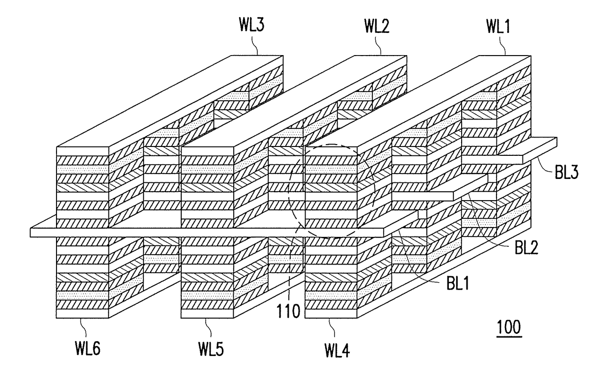
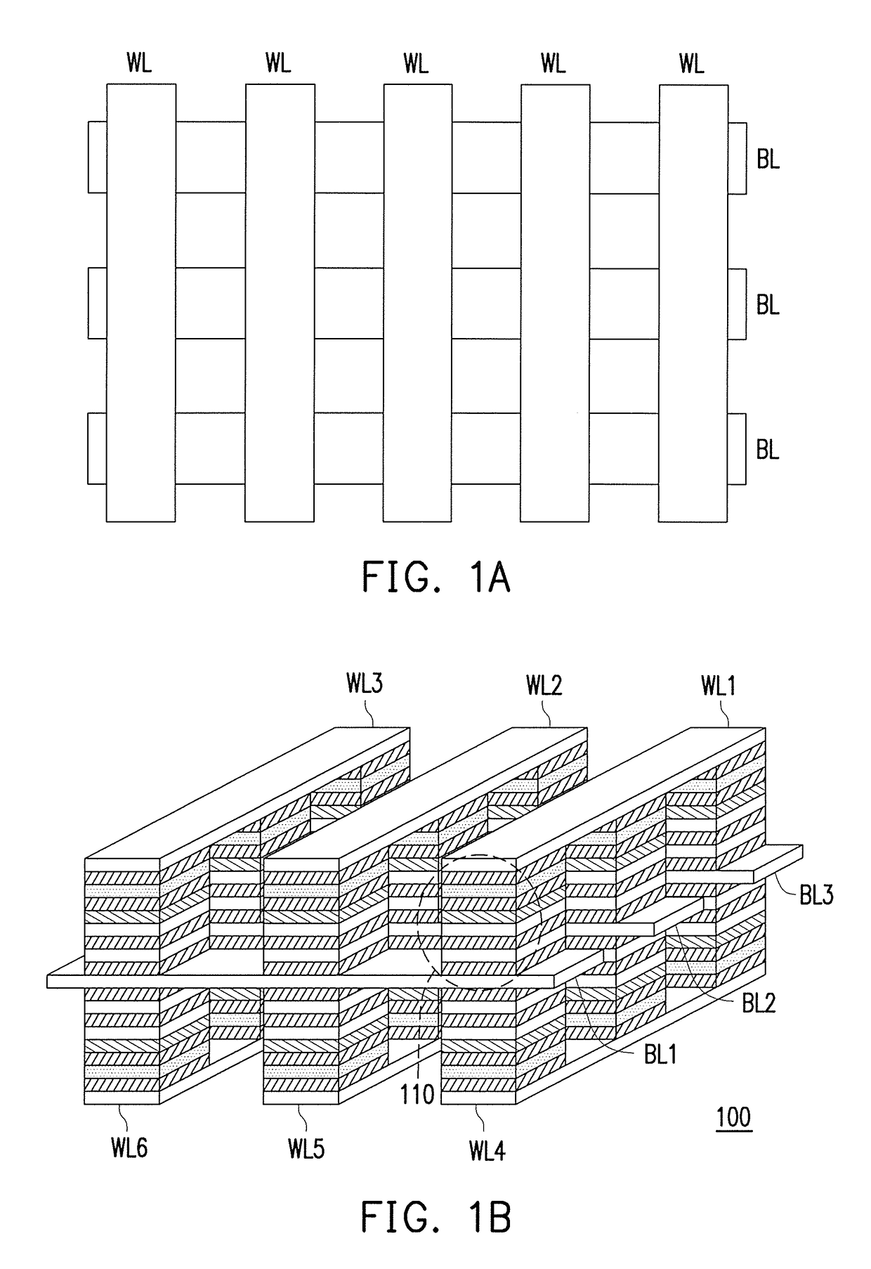
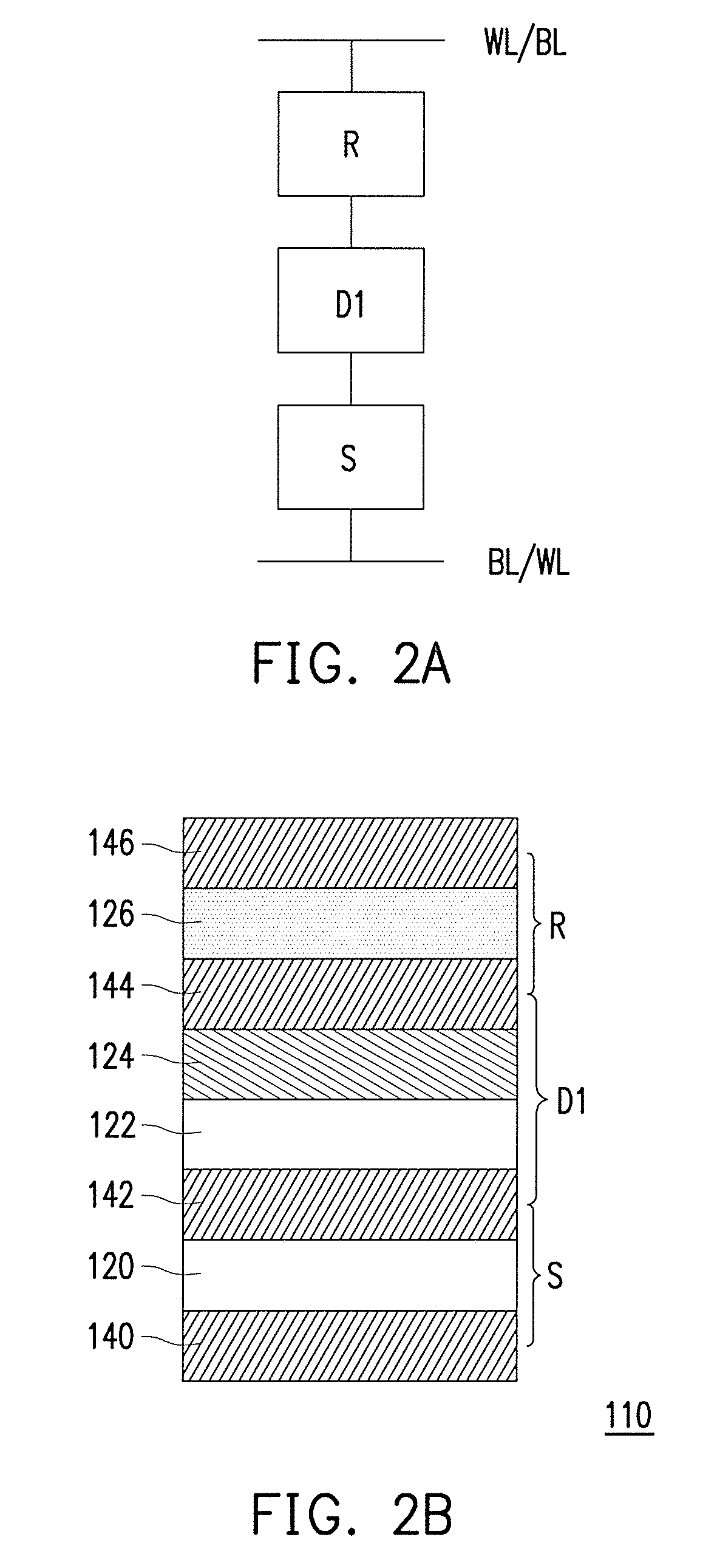
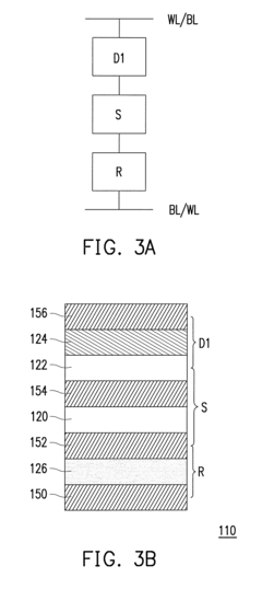
- The resistive random access memory device is designed with a memory cell structure that includes a selector structure, a current limiter structure, and a resistor structure in series, using specific conductive and material layers to reduce dimensions and enhance integration, replacing the traditional 1T1R structure with a 1R1D or 1D1S structure.
Resistive random access memory and memory mini-array thereof with improved reliability
PatentPendingUS20250046372A1
Innovation
- The proposed memory design includes a configuration of switch transistors and resistive memory elements, where each resistive memory element is connected to switch transistors in a specific manner to simplify electrode configurations and enhance reliability. This design allows for improved resistance distinction and reduced memory area by sharing bit lines and source lines between memory cells.
Manufacturing Process Integration Considerations
The integration of Resistive RAM (RRAM) into existing semiconductor manufacturing processes presents significant challenges that must be addressed for successful commercialization. Current CMOS fabrication lines require careful adaptation to accommodate RRAM's unique material requirements and structural characteristics. The primary integration approaches include Back-End-Of-Line (BEOL) integration, where RRAM cells are fabricated between metal interconnect layers, and Front-End-Of-Line (FEOL) integration, which incorporates RRAM elements earlier in the process flow.
Temperature compatibility represents a critical consideration, as many RRAM materials require processing temperatures below 400°C to maintain compatibility with BEOL processes. Higher temperatures can damage underlying interconnects or cause undesired diffusion of materials. This thermal budget constraint significantly impacts material selection and deposition techniques, often necessitating the development of specialized low-temperature processes.
Material contamination control presents another major challenge. Many RRAM designs utilize materials not traditionally found in CMOS fabrication, such as hafnium oxide, titanium oxide, or various transition metal oxides. These materials can potentially contaminate standard CMOS equipment, requiring dedicated tools or comprehensive cleaning protocols to prevent cross-contamination that could affect device performance and reliability.
Etching and patterning processes must be carefully optimized for RRAM structures. The diverse material stack in RRAM devices often requires multiple etching steps with different chemistries, creating challenges in achieving precise pattern transfer while maintaining critical dimensions. Plasma damage during etching can also significantly impact the switching properties of the resistive layer, necessitating careful process control.
Interface engineering between different layers in the RRAM stack is crucial for device performance. The quality of interfaces between the electrodes and the switching layer directly influences switching behavior, retention, and endurance characteristics. Advanced deposition techniques such as Atomic Layer Deposition (ALD) are often employed to achieve precise control over these interfaces.
Scaling considerations must address both lateral dimensions and layer thicknesses. As device dimensions shrink, process variations become increasingly significant, potentially causing wider distributions in device parameters. Uniformity control across wafers becomes more challenging at smaller nodes, requiring enhanced process monitoring and control strategies.
Finally, yield management for RRAM manufacturing requires developing specific defect detection and analysis methods tailored to resistive switching mechanisms. Traditional CMOS testing methodologies may not adequately capture RRAM-specific failure modes, necessitating new inspection and characterization techniques to ensure reliable mass production.
Power Efficiency and Scaling Limitations
Power efficiency represents a critical parameter in the development and implementation of Resistive RAM (RRAM) technologies. Current RRAM devices demonstrate significant advantages over conventional memory technologies, with standby power consumption approximately 10-100 times lower than DRAM and active power consumption reduced by factors of 2-5 compared to flash memory. This efficiency stems from the fundamental operating principles of RRAM, which requires energy only during switching operations rather than for state maintenance.
Despite these advantages, several power-related challenges persist in RRAM design. The SET/RESET operations in RRAM cells still demand relatively high current densities, typically in the range of 10^5-10^6 A/cm², which creates localized heating and potential reliability issues. The variability in switching voltages across different cells further complicates power management strategies, requiring conservative voltage margins that reduce overall efficiency.
Scaling limitations present another significant challenge for RRAM technology advancement. While theoretical models suggest RRAM could scale below 10nm node, practical implementations face substantial hurdles. As cell dimensions decrease, the forming voltage paradoxically increases due to reduced filament formation probability in smaller active regions. This contradicts the expected trend of lower operating voltages with scaling and creates fundamental design conflicts.
The sneak path current problem intensifies with scaling, as leakage currents through unselected cells in crossbar arrays become proportionally larger relative to the intended read current. This phenomenon necessitates complex selector devices that add to the overall cell footprint and partially negate the density advantages of scaling. Current selector technologies introduce additional voltage drops of 0.7-1.2V, significantly impacting the power budget of low-voltage RRAM operations.
Material interface effects become increasingly dominant at smaller scales, with electron tunneling and quantum confinement phenomena altering the expected behavior of traditional semiconductor models. The thickness of the switching layer approaches atomic dimensions at advanced nodes (sub-5nm), where discrete atomic movements rather than continuous processes govern switching behavior, introducing fundamental physical limitations to predictable operation.
Industry roadmaps suggest that overcoming these power efficiency and scaling limitations will require interdisciplinary approaches combining materials science innovations, novel device architectures, and advanced circuit techniques. Promising directions include engineered interface layers to control filament formation, three-dimensional integration strategies to circumvent two-dimensional scaling limits, and hybrid selector-memory structures that minimize parasitic effects while maintaining manufacturability.
Unlock deeper insights with PatSnap Eureka Quick Research — get a full tech report to explore trends and direct your research. Try now!
Generate Your Research Report Instantly with AI Agent
Supercharge your innovation with PatSnap Eureka AI Agent Platform!