The Role of Patents in Shaping Resistive RAM's Future
OCT 9, 20259 MIN READ
Generate Your Research Report Instantly with AI Agent
Patsnap Eureka helps you evaluate technical feasibility & market potential.
ReRAM Technology Background and Objectives
Resistive Random Access Memory (ReRAM) has emerged as a promising non-volatile memory technology in the semiconductor industry over the past two decades. The evolution of ReRAM technology can be traced back to the early 2000s when researchers began exploring alternative memory solutions to address the scaling limitations of conventional flash memory. ReRAM's fundamental operating principle relies on the resistance switching phenomenon in metal-oxide materials, where the application of electrical voltage induces a change in resistance state that can be used to store binary information.
The technology landscape has witnessed significant advancements in ReRAM development, progressing from basic proof-of-concept demonstrations to sophisticated multi-layer architectures capable of high-density storage. This evolution has been driven by the increasing demand for faster, more energy-efficient, and higher capacity memory solutions in various applications ranging from consumer electronics to data centers and emerging edge computing devices.
Patent activities in the ReRAM domain have shown exponential growth since 2010, with major semiconductor companies and research institutions filing thousands of patents covering materials, device structures, fabrication processes, and integration schemes. These patents have played a crucial role in shaping the technology roadmap and commercial deployment strategies for ReRAM, creating both opportunities and barriers for market entrants.
The primary technical objectives for ReRAM development include achieving higher storage density, improved switching reliability, reduced power consumption, and enhanced endurance characteristics. Additionally, there is a growing focus on developing multi-bit storage capabilities and 3D integration techniques to maximize storage capacity within limited chip area. These objectives align with the broader industry goals of developing memory technologies that can support the increasing data processing requirements of artificial intelligence, Internet of Things, and big data applications.
Current research trends indicate a shift towards exploring novel material systems beyond traditional metal oxides, including perovskites, chalcogenides, and two-dimensional materials. These materials offer potential advantages in terms of switching speed, energy efficiency, and compatibility with advanced semiconductor manufacturing processes. Patent activities in these emerging material systems have been increasing, suggesting a strategic pivot in the research and development focus of key industry players.
The patent landscape analysis reveals that intellectual property strategies are increasingly focused on application-specific optimizations of ReRAM technology, particularly for neuromorphic computing, in-memory computing, and security applications. This trend reflects the growing recognition of ReRAM's potential beyond conventional data storage, positioning it as an enabling technology for next-generation computing paradigms that demand high-performance, energy-efficient memory solutions.
Market Demand Analysis for ReRAM Solutions
The global market for Resistive Random Access Memory (ReRAM) solutions is experiencing significant growth, driven by increasing demands for more efficient, high-performance memory technologies. Current market projections indicate that the ReRAM market is expected to grow at a compound annual growth rate of 16% between 2023 and 2030, reaching approximately 2.4 billion USD by the end of the forecast period.
The primary market demand for ReRAM stems from its potential to address critical limitations in existing memory technologies. Data centers and cloud computing infrastructure providers are actively seeking energy-efficient memory solutions that can handle the exponential growth in data processing requirements while minimizing power consumption. ReRAM's non-volatile nature and low power operation make it particularly attractive for these applications.
Consumer electronics represents another substantial market segment, with smartphone manufacturers exploring ReRAM as a potential replacement for flash memory in high-end devices. The demand is driven by ReRAM's faster write speeds, higher endurance, and lower power consumption compared to conventional flash memory. This market segment is expected to grow as ReRAM technology matures and production costs decrease.
The automotive industry is emerging as a promising market for ReRAM solutions, particularly with the rise of autonomous vehicles and advanced driver assistance systems. These applications require memory technologies that can operate reliably under extreme temperature conditions and withstand high radiation environments, characteristics where ReRAM demonstrates significant advantages over competing technologies.
Industrial IoT applications constitute another growing market segment for ReRAM. The technology's radiation hardness, temperature stability, and low power consumption make it ideal for sensors and edge computing devices deployed in harsh industrial environments. Market analysis indicates that this segment could represent up to 15% of the total ReRAM market by 2028.
Patent activity in the ReRAM space correlates strongly with market demand trends. Analysis of patent filings over the past decade reveals increasing interest in ReRAM applications for neuromorphic computing and artificial intelligence accelerators. This suggests that the market is anticipating significant demand for memory solutions optimized for AI workloads, where ReRAM's ability to perform in-memory computing offers substantial performance and energy efficiency advantages.
The geographical distribution of market demand shows Asia-Pacific leading in adoption, followed by North America and Europe. China and South Korea, in particular, are investing heavily in ReRAM development, driven by national semiconductor strategies and the presence of major memory manufacturers. This regional demand pattern is reflected in patent filing activities, with Asian companies holding a substantial portion of ReRAM-related intellectual property.
Current ReRAM Patent Landscape and Challenges
The current ReRAM patent landscape reveals a highly competitive and rapidly evolving technological battlefield. As of 2023, over 5,000 patents related to Resistive RAM technologies have been filed globally, with a significant acceleration in filing rates observed since 2015. This surge indicates the growing recognition of ReRAM's potential to revolutionize the non-volatile memory market.
Major patent holders include established semiconductor companies like Samsung, Micron, and Intel, alongside specialized memory manufacturers such as Crossbar, Weebit Nano, and Adesto Technologies. These entities have strategically built robust patent portfolios covering fundamental ReRAM mechanisms, materials, fabrication processes, and integration techniques. The geographical distribution of patents shows concentration in the United States, South Korea, Japan, China, and Taiwan, reflecting the global centers of semiconductor innovation.
A critical challenge in the ReRAM patent landscape is the existence of overlapping claims and potential patent thickets, particularly regarding switching mechanisms and material compositions. This creates significant barriers for new entrants and increases litigation risks for existing players. Several high-profile patent disputes have already emerged, notably between Crossbar and Micron regarding filamentary switching mechanisms.
Material innovation patents represent a particularly contentious area, with competing claims on metal oxide compositions, interface engineering, and doping strategies. These patents are crucial as they directly impact device performance metrics such as endurance, retention, and switching speed. Similarly, integration patents covering 3D architectures and CMOS compatibility have become increasingly valuable as commercialization efforts intensify.
The patent landscape also reveals significant challenges in standardization. The diversity of ReRAM technologies and approaches has led to fragmented intellectual property ownership, complicating industry-wide adoption and interoperability. This fragmentation has slowed commercialization despite the technology's promising characteristics.
Another notable challenge is the gap between patented concepts and commercially viable implementations. Many patents describe theoretical structures or processes that face significant manufacturing hurdles when scaled to production volumes. This disconnect between intellectual property and practical implementation represents a critical barrier to ReRAM's widespread market penetration.
Looking forward, patent activity suggests emerging focus areas including neuromorphic computing applications, multi-bit storage capabilities, and novel selector devices for crossbar arrays. These areas likely represent the next frontiers for ReRAM innovation and commercial differentiation, with patent positioning becoming increasingly strategic for market participants.
Current ReRAM Patent Strategies
01 RRAM Device Structure and Materials
Resistive RAM devices utilize specific materials and structures to enable resistive switching behavior. These devices typically consist of a metal-insulator-metal structure where the insulator layer can be switched between high and low resistance states. Various materials such as metal oxides, chalcogenides, and perovskites are used as the switching medium. The structure may include additional layers for improved performance, such as barrier layers, electrode materials with specific properties, and doped regions to control ion migration.- RRAM device structures and fabrication methods: Various device structures and fabrication methods for Resistive Random Access Memory (RRAM) have been developed to enhance performance and reliability. These include specific electrode materials, resistive switching layers, and manufacturing techniques that optimize the formation and operation of memory cells. The designs focus on improving switching characteristics, endurance, and integration with existing semiconductor processes.
- Switching mechanisms and materials for RRAM: Research on resistive switching mechanisms and materials is crucial for RRAM development. Various metal oxides, chalcogenides, and other materials exhibit resistive switching behavior suitable for memory applications. The selection of materials affects key performance parameters such as switching speed, power consumption, and retention time. Understanding the physical mechanisms behind resistive switching enables the design of more efficient memory devices.
- RRAM array architectures and integration: Various array architectures have been developed for RRAM implementation, including crossbar arrays, 3D stacking, and integration with selector devices. These architectures address challenges such as sneak path currents, cell density, and compatibility with peripheral circuitry. Integration approaches focus on combining RRAM with conventional CMOS technology to create hybrid memory systems that leverage the advantages of both technologies.
- RRAM operation and control methods: Advanced operation and control methods for RRAM devices include specific programming, erasing, and reading schemes that optimize performance and reliability. These methods involve precise control of voltage pulses, current compliance, and timing parameters to achieve consistent switching behavior. Techniques such as forming, set, reset, and read operations are designed to extend device lifetime while maintaining data integrity and reducing power consumption.
- Multi-level cell and neuromorphic applications of RRAM: RRAM technology enables multi-level cell (MLC) storage and neuromorphic computing applications due to its analog switching characteristics. MLC implementations increase memory density by storing multiple bits per cell through precise control of resistance states. In neuromorphic applications, RRAM devices can emulate synaptic functions for artificial neural networks, enabling efficient hardware implementation of brain-inspired computing architectures with low power consumption and high parallelism.
02 RRAM Operation and Switching Mechanisms
The operation of RRAM devices involves switching between high and low resistance states through various mechanisms. These mechanisms include filament formation and rupture, ion migration, and interface effects. The switching can be controlled by applying appropriate voltage pulses that cause localized changes in the resistive material. Different operational modes such as unipolar and bipolar switching are employed depending on the device design and material system. Understanding and controlling these mechanisms is crucial for reliable device operation and performance optimization.Expand Specific Solutions03 RRAM Integration and Fabrication Techniques
Integration of RRAM devices into semiconductor manufacturing processes involves specific fabrication techniques and compatibility considerations. These include methods for depositing uniform resistive layers, patterning techniques for high-density arrays, and processes for forming reliable contacts. Advanced fabrication approaches such as atomic layer deposition, reactive sputtering, and precise etching methods are employed to create nanoscale RRAM structures. Integration with CMOS technology and 3D stacking techniques enables high-density memory arrays and embedded applications.Expand Specific Solutions04 RRAM Circuit Design and Array Architecture
Circuit designs and array architectures for RRAM implementation focus on addressing, sensing, and control schemes. These include crossbar arrays, 1T1R (one transistor, one resistor) configurations, and various selector devices to mitigate sneak path issues. Peripheral circuits for programming, reading, and erasing operations are designed to provide appropriate voltage/current conditions while minimizing power consumption. Advanced architectures incorporate features for error correction, wear leveling, and multi-level cell operation to enhance memory density and reliability.Expand Specific Solutions05 RRAM Applications and System Integration
RRAM technology finds applications in various computing paradigms and memory systems. These include non-volatile memory replacement, storage class memory, and neuromorphic computing applications that leverage the analog nature of resistive switching. RRAM devices are integrated into systems for in-memory computing, edge AI accelerators, and IoT devices where low power and non-volatility are critical. The technology enables new computing architectures that overcome the memory-processor bottleneck through computational memory approaches and brain-inspired computing systems.Expand Specific Solutions
Key Patent Holders and Industry Competitors
The Resistive RAM (RRAM) market is currently in a transitional phase, moving from research to early commercialization, with an estimated market size of $300-500 million that is projected to grow significantly as the technology matures. Major semiconductor manufacturers including Samsung Electronics, SK Hynix, and Taiwan Semiconductor Manufacturing Co. are investing heavily in RRAM development, while specialized players like CrossBar and TetraMem are focusing on innovative applications. Patent activity reveals a competitive landscape where established memory giants (Micron, Intel) compete with research institutions (Institute of Microelectronics of Chinese Academy of Sciences, Peking University) for intellectual property dominance. The technology is approaching commercial viability for specific applications, with companies like KIOXIA and Winbond Electronics developing products for embedded systems and IoT devices where RRAM's low power consumption provides competitive advantages.
Taiwan Semiconductor Manufacturing Co., Ltd.
Technical Solution: TSMC has developed a significant patent portfolio around ReRAM manufacturing integration and process technology. As the world's leading semiconductor foundry, TSMC's patents focus on embedding ReRAM into their advanced logic processes, enabling system-on-chip solutions with integrated non-volatile memory. Their approach includes specialized back-end-of-line (BEOL) integration methods that maintain ReRAM performance while ensuring compatibility with existing CMOS fabrication flows. TSMC has patented unique barrier layers and interface engineering techniques that prevent contamination between ReRAM materials and traditional interconnect structures. Their intellectual property covers specialized etching and deposition processes for creating uniform switching layers at advanced nodes, addressing critical challenges in ReRAM scaling[4][7]. TSMC's patents also extend to reliability enhancement techniques, including specialized encapsulation methods and thermal budget management during processing. Recent patent filings indicate development of ReRAM-based computing-in-memory architectures optimized for edge AI applications, leveraging their ability to integrate memory and logic functions.
Strengths: TSMC's position as the leading foundry gives them unique advantages in establishing ReRAM manufacturing standards and integration approaches. Their partnerships with multiple ReRAM developers allow them to incorporate diverse technological approaches. Weaknesses: As a foundry, TSMC may be more focused on process integration than fundamental ReRAM materials innovation, potentially limiting their influence on core technology development. Their business model requires partnerships with design companies to fully commercialize ReRAM solutions.
Samsung Electronics Co., Ltd.
Technical Solution: Samsung has developed a comprehensive patent portfolio for Resistive RAM (ReRAM) technology, focusing on innovative cell structures and manufacturing processes. Their approach includes multi-layer cross-point architectures that enable high-density memory arrays with improved scalability. Samsung's ReRAM patents cover specialized materials for switching layers, including metal oxides with engineered oxygen vacancy distributions that enhance switching reliability and endurance. The company has also patented unique selector devices to minimize sneak path currents in high-density arrays, addressing one of ReRAM's key challenges. Their integration methods for embedding ReRAM into logic processes have been critical for enabling neuromorphic computing applications, with patents covering specific programming schemes that optimize weight updates in neural network implementations[1][3]. Samsung's patent strategy extends to 3D integration techniques that stack multiple ReRAM layers, potentially achieving storage densities comparable to 3D NAND while maintaining ReRAM's speed advantages.
Strengths: Samsung's extensive manufacturing infrastructure and integration expertise give them significant advantages in commercializing ReRAM technology. Their cross-licensing agreements with other major players strengthen their freedom to operate. Weaknesses: Despite strong patent positions, Samsung faces challenges in achieving cost parity with established memory technologies, and some of their early ReRAM patents will begin expiring in the coming years, potentially weakening their competitive position.
Critical Patents and Technical Innovations
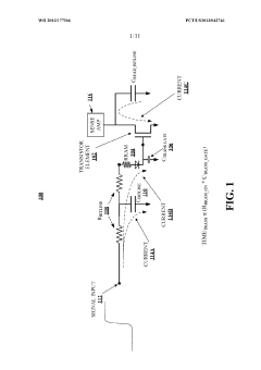
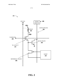
High operating speed resistive random access memory
PatentWO2013177566A1
Innovation
- The development of a high-speed RRAM architecture that connects multiple RRAM devices to a single read transistor, utilizing a reference transistor to apply a bias voltage and mitigate off-current, and employing a sensing circuit to quickly detect changes in electrical characteristics, enabling fast programming, reading, and erasing operations while reducing the number of read transistors and associated circuitry.
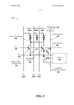
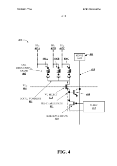
High retention resistive random access memory
PatentActiveUS20180309054A1
Innovation
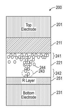
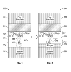
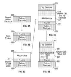
- An RRAM stack is enhanced with an additional oxide thin film layer at the interface between the electrode and oxide, stabilizing oxygen vacancy migration and retention, allowing for reliable switching between high and low resistive states.
IP Monetization and Licensing Strategies
In the rapidly evolving landscape of Resistive RAM (ReRAM) technology, intellectual property (IP) monetization and licensing strategies have become critical components for market players seeking to capitalize on their innovations. The patent ecosystem surrounding ReRAM has matured significantly, creating diverse opportunities for revenue generation beyond traditional product sales. Companies holding strategic ReRAM patents can implement multi-tiered licensing programs that cater to different market segments, from semiconductor manufacturers to end-device producers.
Cross-licensing agreements have emerged as particularly valuable in the ReRAM sector, allowing companies to access complementary technologies while reducing litigation risks. These arrangements facilitate technology integration across the memory hierarchy and enable the development of hybrid memory solutions that combine ReRAM with established technologies like DRAM and NAND flash. The strategic value of such agreements increases as ReRAM approaches wider commercial adoption.
Patent pools represent another significant monetization avenue, especially beneficial for standardizing ReRAM interfaces and protocols. By aggregating essential patents from multiple holders, these pools streamline licensing processes and reduce transaction costs for implementers. Several industry consortia are currently exploring the formation of ReRAM-specific patent pools to accelerate market adoption while ensuring fair compensation for innovators.
Territorial licensing strategies have gained importance as ReRAM manufacturing and implementation vary across global regions. Companies are increasingly tailoring their licensing terms to account for regional market differences, regulatory environments, and manufacturing capabilities. This approach maximizes revenue potential while accommodating the varying stages of ReRAM adoption worldwide.
Value-based licensing models are replacing traditional unit-based approaches, particularly for ReRAM applications in emerging fields like neuromorphic computing and in-memory processing. These models tie licensing fees to the value created by the technology rather than simply counting implementation instances, allowing patent holders to capture a fair share of the economic benefits their innovations enable.
For startups and research institutions with promising ReRAM IP portfolios but limited manufacturing capabilities, IP transfer and acquisition have become viable monetization paths. Established semiconductor companies actively seek to acquire strategic ReRAM patents to strengthen their competitive positions, creating lucrative exit opportunities for smaller entities focused on fundamental research and early-stage development.
Legal and Standardization Implications
The patent landscape surrounding Resistive RAM (RRAM) technology has created a complex legal environment that significantly impacts industry development. Patent thickets have emerged as major corporations and research institutions aggressively protect their intellectual property, creating potential barriers to market entry for smaller players. These dense networks of overlapping patent rights necessitate extensive licensing agreements and cross-licensing arrangements, which have become standard practice among established RRAM developers.
Standardization efforts for RRAM technology face considerable challenges due to this fragmented patent landscape. Industry consortia such as JEDEC and IEEE have attempted to establish technical standards, but progress has been hampered by competing proprietary technologies protected by different patent portfolios. The absence of unified standards has led to market fragmentation, with incompatible RRAM implementations limiting interoperability and broader adoption.
Legal disputes over RRAM patents have increased in recent years, with several high-profile infringement cases reaching courts globally. These litigation battles not only consume substantial resources but also create uncertainty in the market, potentially deterring investment in RRAM commercialization. The resolution of these disputes often results in settlement agreements that further concentrate patent rights among dominant players.
Patent pooling has emerged as a potential solution to mitigate these challenges. Several initiatives aim to create patent pools specific to RRAM technology, allowing more equitable access to essential patents through standardized licensing terms. However, participation remains voluntary, and key patent holders may choose to maintain exclusive control over their intellectual property to preserve competitive advantages.
International variations in patent law add another layer of complexity. Different interpretations of patentability criteria for semiconductor technologies across jurisdictions create inconsistent protection levels globally. This regulatory fragmentation complicates multinational RRAM development strategies and may lead to regional technology divergence based on local patent environments.
Open innovation approaches are gaining traction as an alternative pathway. Some academic institutions and companies have begun releasing certain RRAM-related innovations under open-source licenses or through defensive publication strategies. These initiatives aim to create patent-free zones within the RRAM ecosystem, potentially accelerating innovation in specific areas while circumventing patent barriers.
The future standardization of RRAM will likely require balanced approaches that respect legitimate intellectual property rights while ensuring sufficient access to enable industry growth. Regulatory bodies may need to intervene with policies that promote fair, reasonable, and non-discriminatory (FRAND) licensing terms for standard-essential patents in the RRAM domain.
Unlock deeper insights with Patsnap Eureka Quick Research — get a full tech report to explore trends and direct your research. Try now!
Generate Your Research Report Instantly with AI Agent
Supercharge your innovation with Patsnap Eureka AI Agent Platform!