What Drives Resistive RAM Advances in Electronics
OCT 9, 202510 MIN READ
Generate Your Research Report Instantly with AI Agent
Patsnap Eureka helps you evaluate technical feasibility & market potential.
RRAM Technology Evolution and Objectives
Resistive Random Access Memory (RRAM) has emerged as a promising technology in the landscape of non-volatile memory solutions, offering significant advantages over conventional memory technologies. The evolution of RRAM can be traced back to the early 2000s when researchers began exploring alternative memory technologies to address the limitations of flash memory, particularly in terms of scaling, power consumption, and endurance.
The fundamental principle behind RRAM involves the formation and disruption of conductive filaments within an insulating dielectric layer, enabling the storage of binary information through changes in resistance states. This mechanism allows for faster switching speeds, lower power consumption, and potentially higher density compared to traditional memory technologies.
Over the past two decades, RRAM technology has progressed through several developmental phases. Initially, research focused on understanding the basic switching mechanisms and material compatibility. This was followed by efforts to improve reliability, endurance, and retention characteristics. More recently, the focus has shifted towards scaling, 3D integration, and addressing variability issues to enable commercial viability.
The global semiconductor industry has recognized RRAM as a key technology for next-generation memory applications, particularly in emerging fields such as Internet of Things (IoT), artificial intelligence, and edge computing. These applications demand memory solutions that combine non-volatility, high speed, low power consumption, and compatibility with standard CMOS processes.
Current technological objectives for RRAM development include achieving higher density through multi-level cell capabilities, improving switching uniformity and reliability, reducing operating voltages, and enhancing endurance beyond 10^12 cycles. Additionally, researchers are exploring novel materials and device architectures to overcome existing limitations and expand the application scope of RRAM.
The integration of RRAM with conventional CMOS technology represents another critical objective, as it would enable the development of embedded memory solutions and potentially new computing paradigms such as in-memory computing and neuromorphic systems. These approaches could significantly reduce the energy consumption associated with data movement in conventional von Neumann architectures.
Industry roadmaps suggest that RRAM could play a pivotal role in addressing the memory wall challenge, which has become increasingly problematic as computing performance continues to outpace memory access speeds. By providing fast, non-volatile memory that can be placed closer to processing units, RRAM could help bridge this gap and enable more efficient computing systems.
Looking forward, the trajectory of RRAM technology is expected to continue towards greater integration with logic circuits, improved performance metrics, and expanded functionality beyond simple binary storage. The ultimate goal is to establish RRAM as a universal memory solution that combines the best attributes of existing memory technologies while eliminating their respective limitations.
Market Demand Analysis for Non-Volatile Memory
The non-volatile memory (NVM) market is experiencing significant growth driven by the increasing demand for data storage solutions across multiple industries. Current projections indicate the global NVM market will reach approximately $100 billion by 2025, with a compound annual growth rate exceeding 10%. This growth trajectory is primarily fueled by the expanding applications in consumer electronics, automotive systems, enterprise storage, and emerging Internet of Things (IoT) devices.
Resistive RAM (ReRAM) represents a particularly promising segment within the broader NVM landscape. As traditional memory technologies approach their physical scaling limits, ReRAM offers compelling advantages that address critical market needs. The demand for ReRAM is being propelled by several key factors in the electronics industry.
Power efficiency has become a paramount concern across all electronic applications. ReRAM's non-volatile nature enables persistent data storage without continuous power consumption, making it ideal for energy-constrained applications such as mobile devices, wearables, and IoT sensors. Market research indicates that power consumption in electronic devices could be reduced by up to 30% through widespread adoption of ReRAM technology.
The explosion of data-intensive applications, including artificial intelligence and machine learning, has created unprecedented demand for high-speed, high-density memory solutions. ReRAM's potential for multi-level cell storage and crossbar array architecture positions it as a strong candidate to meet these requirements, with theoretical density improvements of 4-8 times compared to conventional flash memory.
Automotive and industrial markets are increasingly seeking memory solutions capable of operating reliably in harsh environments. ReRAM's demonstrated resilience to temperature extremes, radiation, and electromagnetic interference makes it particularly attractive for these applications, where the market is growing at nearly 15% annually.
The integration of computing and memory functions represents another significant market driver. ReRAM's ability to perform in-memory computing addresses the von Neumann bottleneck that limits conventional computing architectures. This capability is especially valuable for edge computing applications, where processing must occur closer to data sources to reduce latency and bandwidth requirements.
Consumer electronics manufacturers are constantly pursuing thinner, lighter devices with improved performance. ReRAM's compatibility with back-end-of-line processing enables 3D integration, supporting the development of higher-density memory in smaller form factors. This aligns perfectly with the market trend toward increasingly compact yet powerful electronic devices.
As data security concerns intensify across all sectors, ReRAM's potential for implementing hardware-level security features presents another compelling market advantage. The physical properties of resistive switching can be leveraged for physically unclonable functions and true random number generation, addressing growing demand for embedded security solutions.
Current RRAM Development Status and Barriers
Resistive Random Access Memory (RRAM) has emerged as a promising next-generation non-volatile memory technology, offering advantages in scalability, power efficiency, and integration capabilities. Currently, RRAM development has reached a critical juncture with significant progress in materials science, fabrication techniques, and device architecture optimization.
Commercial deployment of RRAM remains limited despite research advancements. Several companies including Crossbar, Weebit Nano, and Fujitsu have demonstrated working prototypes, while some have begun small-scale production for specific applications. However, mass market penetration faces substantial barriers compared to established memory technologies like NAND flash and DRAM.
The primary technical challenges hindering widespread RRAM adoption include reliability issues, particularly related to endurance limitations. Most current RRAM devices achieve 10^6 to 10^9 write cycles, falling short of the 10^12+ cycles required for universal memory applications. Retention characteristics also present concerns, with data preservation capabilities degrading under elevated temperatures or after repeated cycling operations.
Device-to-device and cycle-to-cycle variability represents another significant obstacle. The stochastic nature of filament formation in oxide-based RRAM creates inconsistencies in switching parameters, complicating circuit design and limiting yield rates in manufacturing environments. This variability increases as device dimensions shrink below 20nm, presenting scaling challenges.
Power consumption during the SET operation remains higher than ideal for many mobile and IoT applications. While RESET operations have achieved reasonable efficiency, the overall power profile needs improvement to compete with established technologies. Additionally, the relatively high operating voltages (typically 1-3V) complicate integration with advanced CMOS processes operating at lower voltages.
From a manufacturing perspective, integration with standard CMOS processes presents compatibility challenges. While RRAM offers theoretical back-end-of-line (BEOL) integration advantages, practical implementation requires addressing thermal budget constraints and material contamination risks. The industry lacks standardized fabrication processes, resulting in significant variations in device performance across different manufacturing facilities.
Geographically, RRAM research and development shows distinct patterns. Asian institutions and companies, particularly in China, Japan, and South Korea, lead in patent filings and material science innovations. North American entities focus more on circuit design and system architecture, while European research centers contribute significantly to fundamental understanding of switching mechanisms and reliability physics.
The current technological landscape suggests RRAM will likely find initial commercial success in specialized applications rather than as a universal memory solution. Embedded non-volatile memory for microcontrollers, neuromorphic computing elements, and select storage class memory applications represent the most promising near-term opportunities as researchers continue addressing the fundamental barriers to broader adoption.
Current RRAM Architecture and Implementation Approaches
01 Novel materials and structures for RRAM devices
Recent advances in RRAM technology include the development of novel materials and device structures to enhance performance. These innovations involve using various metal oxides, two-dimensional materials, and engineered interfaces to improve switching characteristics. Multi-layer structures with carefully selected materials have shown improved retention, endurance, and reliability. These novel material systems enable better control over the formation and rupture of conductive filaments that are fundamental to RRAM operation.- Novel materials and structures for RRAM devices: Advanced materials and innovative structures are being developed to enhance RRAM performance. These include the use of novel metal oxides, two-dimensional materials, and engineered interfaces that improve switching characteristics. Multi-layer structures with carefully designed material combinations can provide better control over resistive switching mechanisms, resulting in improved reliability, endurance, and retention properties of RRAM devices.
- Fabrication techniques for RRAM optimization: Innovative fabrication methods are being developed to optimize RRAM performance. These techniques include atomic layer deposition, plasma treatment processes, and precise control of defect engineering. Advanced manufacturing approaches enable the creation of uniform switching layers with controlled oxygen vacancy distribution, which is crucial for consistent RRAM operation. These fabrication advancements lead to devices with improved switching characteristics and reduced variability.
- Integration of RRAM with CMOS technology: Significant advances have been made in integrating RRAM with conventional CMOS technology to create high-density memory arrays. This integration enables the development of embedded non-volatile memory solutions that combine the benefits of RRAM with traditional semiconductor manufacturing processes. The CMOS-compatible fabrication approaches allow for 3D stacking of memory cells, back-end-of-line integration, and the creation of hybrid computing architectures that leverage both technologies.
- Circuit design and programming schemes for RRAM: Advanced circuit designs and programming schemes are being developed to address the challenges of RRAM operation. These include innovative sensing circuits, multi-level cell programming techniques, and error correction methods. Specialized programming algorithms help mitigate issues like resistance drift and variability, while novel read schemes improve the reliability of data retrieval. These circuit-level innovations are essential for realizing the full potential of RRAM technology in practical applications.
- Neuromorphic computing applications of RRAM: RRAM devices are increasingly being utilized for neuromorphic computing applications due to their ability to mimic synaptic behavior. The analog switching characteristics of RRAM cells make them suitable for implementing artificial neural networks in hardware. These devices can perform weight updates and signal processing directly in memory, enabling efficient implementation of brain-inspired computing architectures. This approach offers significant advantages in terms of energy efficiency and processing speed for artificial intelligence applications.
02 Integration and fabrication techniques for RRAM
Advanced fabrication and integration techniques have been developed to incorporate RRAM into existing semiconductor manufacturing processes. These include methods for creating high-density memory arrays, 3D stacking approaches, and techniques compatible with back-end-of-line processing. Innovations in deposition methods, etching processes, and interface engineering have enabled the production of more reliable and scalable RRAM devices. These fabrication advances are crucial for the commercial viability of RRAM technology.Expand Specific Solutions03 Circuit design and operational improvements for RRAM
Circuit-level innovations have significantly enhanced RRAM performance and functionality. These include novel sensing schemes, programming algorithms, and peripheral circuitry designs that improve read/write operations. Advanced circuit techniques address challenges such as sneak path currents in crossbar arrays and variability in switching behavior. Pulse shaping methods and adaptive programming approaches have been developed to optimize the trade-off between speed, power consumption, and reliability, making RRAM more suitable for various applications.Expand Specific Solutions04 Multi-level cell and neuromorphic applications of RRAM
RRAM technology has been extended to support multi-level cell operation and neuromorphic computing applications. By precisely controlling the resistance states, multiple bits can be stored in a single memory cell, increasing storage density. The analog nature of resistance switching in RRAM makes it particularly suitable for implementing artificial neural networks and neuromorphic systems. These devices can emulate synaptic behavior, enabling efficient hardware implementation of machine learning algorithms with significantly reduced power consumption compared to conventional computing architectures.Expand Specific Solutions05 Reliability and endurance enhancement techniques
Significant progress has been made in addressing reliability and endurance challenges in RRAM technology. These advances include methods to control filament formation, reduce variability between cycles, and prevent degradation mechanisms. Techniques such as doping, interface engineering, and optimized programming schemes have been developed to extend device lifetime and maintain consistent performance over numerous write cycles. Additionally, error correction methods and redundancy approaches at both device and system levels have been implemented to improve overall reliability.Expand Specific Solutions
Leading Companies and Research Institutions in RRAM
Resistive RAM (RRAM) technology is currently in the early growth phase of its development cycle, characterized by increasing commercial interest amid ongoing research advancements. The global RRAM market, estimated at approximately $310 million in 2023, is projected to grow significantly as applications expand in IoT, AI, and edge computing sectors. Leading semiconductor companies including Samsung Electronics, Intel, Micron Technology, and SK hynix are actively developing RRAM solutions, while specialized players like CrossBar and Adesto Technologies focus exclusively on this technology. Academic institutions such as Peking University and Fudan University collaborate with industry partners to overcome technical challenges in scalability, endurance, and retention. The competitive landscape is further shaped by foundry services from TSMC and SMIC, positioning RRAM as a promising next-generation memory technology approaching broader commercial adoption.
Samsung Electronics Co., Ltd.
Technical Solution: Samsung has pioneered resistive RAM (ReRAM) technology with their cross-point architecture that enables high-density memory arrays. Their approach utilizes metal oxide materials (primarily HfO2 and TaOx) for the resistive switching layer, allowing for multi-level cell operation with up to 4 bits per cell. Samsung's ReRAM technology demonstrates excellent endurance (>10^6 cycles), fast switching speeds (<10ns), and low operating voltages (<3V). The company has integrated ReRAM into their advanced semiconductor manufacturing processes, achieving 20nm node implementation with plans for sub-10nm scaling. Samsung has also developed innovative selector devices to mitigate sneak path currents in high-density arrays, significantly improving read accuracy and energy efficiency. Their ReRAM solutions target both standalone memory applications and embedded systems, with particular focus on neuromorphic computing applications where the analog nature of ReRAM can efficiently implement synaptic weights.
Strengths: Industry-leading manufacturing capabilities allow for rapid scaling and integration; extensive materials expertise enables optimization of switching layers; strong IP portfolio in selector technology. Weaknesses: Higher production costs compared to conventional memory; reliability challenges at extreme temperature conditions; requires specialized peripheral circuitry for optimal performance.
Intel Corp.
Technical Solution: Intel's approach to ReRAM technology centers on their 3D XPoint architecture (developed jointly with Micron), which represents one of the most commercially advanced implementations of resistive memory. Their technology utilizes chalcogenide materials with proprietary selector devices arranged in a crossbar structure that enables exceptional density scaling. Intel's ReRAM solution delivers performance characteristics that bridge the gap between DRAM and NAND flash, with access times approximately 10x faster than NAND and endurance ratings 1000x higher. The company has successfully commercialized this technology under the Optane brand, targeting data center applications where low latency and high endurance are critical. Intel's implementation features byte-addressability rather than block-level access, enabling more efficient data operations. Their manufacturing process integrates ReRAM cells between metal interconnect layers, allowing for potential future integration with logic circuits for in-memory computing applications.
Strengths: Established commercial deployment demonstrates technology maturity; performance characteristics fill a critical gap in the memory hierarchy; strong system-level integration with processors. Weaknesses: Higher cost per bit compared to NAND flash; requires specialized controllers and software optimization; manufacturing complexity limits production volume scaling.
Key RRAM Materials and Switching Mechanism Analysis
Setting an upper bound on RRAM resistance
PatentWO2022152601A1
Innovation
- Incorporating a high-resistance semiconductive spacer in parallel with the RRAM module, using materials like TiOxNy or TaxNy, to provide an upper bound on resistance, ensuring proper operation even with manufacturing defects and enhancing stability by encapsulating the filament layer.
Structures for resistive random access memory cells
PatentActiveUS20100110758A1
Innovation
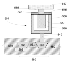
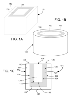
- The RRAM cell design features a trench structure with a first electrode, a resistive layer, and a second electrode that nest inside each other, increasing the contact area between the electrodes and the resistive layer, allowing for larger areal densities and enhanced functioning without increasing the memory chip area.
Integration Challenges with Conventional CMOS Technology
The integration of Resistive RAM (RRAM) with conventional CMOS technology presents significant challenges that must be addressed for successful commercialization. The fundamental issue stems from the material compatibility between RRAM elements and standard CMOS processes. RRAM typically requires metal oxides and specialized electrode materials that are not standard in CMOS fabrication flows, creating process integration difficulties.
Temperature compatibility represents another major hurdle. While CMOS back-end-of-line (BEOL) processes generally require temperatures below 400°C to prevent damage to existing interconnects, some RRAM materials demand higher formation temperatures for optimal performance. This thermal budget constraint limits material selection and processing options for RRAM integration.
Scaling issues further complicate integration efforts. As CMOS technology nodes continue to shrink below 10nm, incorporating RRAM cells while maintaining their performance advantages becomes increasingly difficult. The dimensional constraints impact cell-to-cell variability and reliability, particularly when attempting to achieve high-density memory arrays compatible with advanced CMOS nodes.
Electrical interfacing between RRAM and CMOS transistors presents additional challenges. The selector devices needed to address individual memory cells must be carefully designed to handle the unique current-voltage characteristics of RRAM while maintaining compatibility with standard CMOS voltage levels and signal timing requirements.
Manufacturing yield and reliability concerns also emerge during integration. RRAM devices exhibit cycle-to-cycle and device-to-device variations that can be exacerbated by process variations in the CMOS substrate. Achieving consistent performance across millions of cells on a single chip requires sophisticated process control and potentially new testing methodologies.
The economic aspect of integration cannot be overlooked. Adding RRAM layers to conventional CMOS processes increases manufacturing complexity and cost. The additional masks, process steps, and specialized equipment required must be justified by the performance benefits that RRAM brings to the final system.
Despite these challenges, several promising approaches are being explored. These include developing RRAM-compatible materials that can be processed at lower temperatures, creating specialized interface layers between CMOS and RRAM elements, and designing novel 3D integration schemes that maximize density while minimizing process interference. The development of CMOS-compatible selector devices specifically optimized for RRAM operation also shows potential for addressing the integration challenges.
Energy Efficiency and Scaling Potential of RRAM
Resistive RAM (RRAM) technology has emerged as a promising candidate for next-generation memory solutions due to its remarkable energy efficiency and scaling potential. The power consumption of RRAM devices is significantly lower than conventional memory technologies, with typical write operations requiring only 10-100 pJ per bit, compared to several nJ for flash memory. This energy advantage stems from RRAM's fundamental operating principle, which relies on the formation and disruption of conductive filaments rather than charge storage or movement.
The scaling potential of RRAM is particularly impressive, with demonstrated devices at sub-10 nm feature sizes. Unlike conventional DRAM and flash technologies that face fundamental physical limitations at smaller nodes, RRAM's filamentary switching mechanism remains effective at extremely small dimensions. Recent research has shown functional RRAM cells with feature sizes as small as 5 nm, suggesting a viable path toward ultra-high-density memory arrays.
Energy efficiency in RRAM is further enhanced by its non-volatile nature, eliminating the need for refresh operations that consume significant power in volatile memories like DRAM. This characteristic makes RRAM particularly suitable for energy-constrained applications such as IoT devices and edge computing systems, where standby power consumption is a critical consideration.
The material engineering of RRAM has also contributed to its energy efficiency profile. Metal oxides like HfOx, TaOx, and TiOx have demonstrated excellent resistive switching properties while requiring minimal energy for state transitions. Advanced material stacks incorporating multiple oxide layers have shown improved retention and endurance while maintaining low power operation.
From a scaling perspective, RRAM benefits from its simple two-terminal structure, which allows for high-density 3D integration. Cross-point architectures enable memory densities approaching 10^12 bits/cm², significantly exceeding the practical limits of conventional memory technologies. This architectural advantage, combined with RRAM's inherent scalability, positions it as a strong candidate for storage-class memory applications.
Recent innovations in selector devices have addressed the sneak path current issue in large RRAM arrays, further improving energy efficiency at the system level. Self-rectifying RRAM cells and complementary resistive switches have demonstrated effective current suppression while maintaining the scaling benefits of the technology.
The energy-delay product (EDP) of RRAM continues to improve with each technology generation, with current research devices achieving EDPs orders of magnitude better than flash memory. This metric is particularly important for applications requiring both high performance and low power consumption, such as mobile computing and AI accelerators.
Unlock deeper insights with Patsnap Eureka Quick Research — get a full tech report to explore trends and direct your research. Try now!
Generate Your Research Report Instantly with AI Agent
Supercharge your innovation with Patsnap Eureka AI Agent Platform!