The Landscape of Resistive RAM Patents and Innovations
OCT 9, 20259 MIN READ
Generate Your Research Report Instantly with AI Agent
Patsnap Eureka helps you evaluate technical feasibility & market potential.
ReRAM Technology Background and Objectives
Resistive Random Access Memory (ReRAM) represents a significant advancement in non-volatile memory technology, emerging as a promising alternative to conventional memory solutions. The evolution of ReRAM can be traced back to the early 2000s when researchers began exploring the resistive switching phenomena in various metal oxide materials. This technology leverages the ability of certain materials to change their resistance state when subjected to electrical stimuli, enabling data storage through resistance variations rather than electron charges.
The development trajectory of ReRAM has been characterized by progressive improvements in material science, fabrication techniques, and device architectures. Initially, simple metal-insulator-metal structures demonstrated the fundamental concept, which has since evolved into sophisticated multi-layer designs incorporating various oxide materials such as HfOx, TaOx, and TiOx. These advancements have significantly enhanced performance metrics including endurance, retention time, and switching speed.
Market dynamics and technological limitations of existing memory technologies have been primary drivers for ReRAM development. Traditional NAND flash memory faces scaling challenges below 10nm, while DRAM's volatility necessitates constant power consumption. ReRAM addresses these limitations by offering non-volatility, high density, low power consumption, and compatibility with conventional CMOS processes.
The primary technical objectives for ReRAM development include achieving higher storage density, reducing power consumption, improving reliability, and enhancing integration capabilities with existing semiconductor technologies. Researchers aim to achieve write/erase endurance exceeding 10^12 cycles, data retention periods of over 10 years, and switching speeds in the nanosecond range, while maintaining low operating voltages below 1V.
Patent activities in the ReRAM domain have shown exponential growth since 2010, with major semiconductor companies and research institutions filing thousands of patents covering materials, device structures, fabrication methods, and circuit designs. This intellectual property landscape reflects the strategic importance of ReRAM in the future memory hierarchy.
Current research focuses on understanding and controlling the filament formation mechanisms that underlie resistive switching, developing multi-level cell capabilities for increased storage density, and addressing variability issues that affect device reliability. Innovations in selector devices and crossbar architectures are also critical for enabling high-density memory arrays with minimal sneak path currents.
The ultimate goal for ReRAM technology is to establish itself as a universal memory solution that combines the speed of SRAM, the density of NAND flash, and the non-volatility and endurance necessary for next-generation computing systems, particularly in emerging applications such as neuromorphic computing, edge AI, and Internet of Things devices.
Market Demand Analysis for ReRAM Solutions
The global market for Resistive Random Access Memory (ReRAM) solutions is experiencing significant growth, driven by increasing demand for high-performance, energy-efficient memory technologies. Current market projections indicate that the ReRAM market is expected to grow at a compound annual growth rate of over 40% during the 2023-2028 period, with the market value potentially reaching several billion dollars by the end of this forecast period.
The primary market demand for ReRAM stems from its potential to address the limitations of conventional memory technologies. As data-intensive applications continue to proliferate, traditional memory architectures face challenges in meeting performance requirements while maintaining energy efficiency. ReRAM offers a compelling solution with its non-volatile nature, high endurance, fast switching speeds, and low power consumption.
Several key sectors are driving the demand for ReRAM solutions. The consumer electronics industry represents a significant market segment, with manufacturers seeking memory solutions that can enhance device performance while extending battery life. The Internet of Things (IoT) ecosystem is another major driver, as edge devices require efficient memory solutions capable of processing data locally with minimal power consumption.
Enterprise storage systems constitute another substantial market for ReRAM, particularly for applications requiring high-speed data access and processing. The automotive sector is also emerging as a promising market, with advanced driver-assistance systems and autonomous vehicles demanding robust, reliable memory solutions capable of operating in harsh environments.
Geographic analysis reveals varying levels of market demand across regions. North America and Asia-Pacific currently lead in ReRAM adoption, with significant investments in research and development. Europe follows closely, particularly in automotive and industrial applications, while emerging markets show growing interest as they develop their technological infrastructure.
Customer requirements for ReRAM solutions vary across market segments but generally include demands for higher density, improved reliability, enhanced endurance, and competitive pricing compared to established memory technologies. The cost factor remains a significant consideration, as ReRAM must demonstrate clear advantages over existing solutions to justify adoption.
Market research indicates that the integration of ReRAM in neuromorphic computing and AI applications represents a particularly promising growth area. The ability of ReRAM to efficiently implement neural network architectures makes it well-suited for edge AI applications where power efficiency and real-time processing are critical requirements.
ReRAM Development Status and Technical Challenges
Resistive RAM (ReRAM) technology has emerged as a promising candidate for next-generation non-volatile memory solutions, offering advantages in scalability, power consumption, and switching speed. However, the current development status reveals several significant technical challenges that must be addressed before widespread commercial adoption can occur.
The global ReRAM market is currently in a transitional phase between research and commercialization. Major semiconductor companies and research institutions have demonstrated functional ReRAM devices with impressive specifications, yet mass production remains limited. Current estimates value the ReRAM market at approximately $310 million in 2023, with projections suggesting growth to $2.6 billion by 2028, representing a compound annual growth rate of 52.8%.
Material stability presents one of the most critical challenges in ReRAM development. The formation and dissolution of conductive filaments within the switching layer often suffer from variability issues, leading to inconsistent resistance states and reliability concerns. This variability manifests as cycle-to-cycle and device-to-device variations, complicating circuit design and limiting yield rates in manufacturing processes.
Endurance limitations constitute another significant hurdle. While conventional flash memory typically achieves 10^4-10^5 write cycles, ReRAM aims to reach 10^9-10^12 cycles. Current laboratory demonstrations have achieved approximately 10^6-10^8 cycles, but degradation mechanisms including electrode material migration, oxygen vacancy clustering, and interface layer formation continue to restrict long-term reliability.
Retention characteristics present additional challenges, particularly at elevated temperatures. Data retention in ReRAM devices tends to deteriorate significantly above 85°C, falling short of the automotive-grade requirements of 10-year data retention at 125°C. This temperature sensitivity stems from thermally activated ion migration within the switching layer, which can disrupt previously programmed resistance states.
Scaling issues emerge as device dimensions approach sub-20nm nodes. At these dimensions, the stochastic nature of filament formation becomes more pronounced, resulting in wider distributions of switching parameters. Additionally, the reduced number of atoms involved in the switching process increases susceptibility to single-atom defects and thermal fluctuations.
Integration challenges with CMOS technology represent another obstacle. While ReRAM offers potential for back-end-of-line integration, issues including thermal budget constraints, material compatibility, and process contamination concerns have limited seamless integration with standard semiconductor manufacturing flows. Current solutions often require specialized process steps that increase manufacturing complexity and cost.
Current ReRAM Implementation Approaches
01 Materials and structures for RRAM devices
Resistive Random Access Memory (RRAM) devices utilize specific materials and structures to enable resistive switching behavior. These typically include metal oxides like HfO2, TiO2, or Ta2O5 as the switching layer sandwiched between two electrodes. The structure may incorporate additional layers such as barrier layers or doping elements to enhance performance. The specific arrangement of these materials significantly impacts the device's switching characteristics, endurance, and retention properties.- Materials and structures for RRAM devices: Resistive Random Access Memory (RRAM) devices utilize specific materials and structures to achieve resistive switching behavior. These typically include metal oxides like HfO2, TiO2, or Ta2O5 as the switching layer sandwiched between two electrodes. The structure may incorporate additional layers such as barrier layers or doping elements to enhance performance. The specific arrangement of these materials significantly impacts the device's switching characteristics, endurance, and retention properties.
- Switching mechanisms in RRAM: RRAM operates based on resistive switching mechanisms where the resistance of the memory cell can be altered between high and low resistance states. This switching behavior typically occurs through the formation and rupture of conductive filaments within the switching layer. The filaments form due to ion migration, oxygen vacancy movement, or other electrochemical processes under applied electric fields. Understanding and controlling these mechanisms is crucial for optimizing RRAM performance and reliability.
- Integration and fabrication techniques: The fabrication of RRAM devices involves various integration techniques compatible with standard semiconductor manufacturing processes. These include deposition methods for the switching layer such as atomic layer deposition, sputtering, or chemical vapor deposition. Patterning techniques, electrode formation, and 3D integration approaches are also critical aspects. Advanced fabrication methods aim to improve device uniformity, reduce cell size, and enable high-density memory arrays while maintaining compatibility with CMOS technology.
- Circuit design and operation methods: RRAM devices require specific circuit designs and operation methods to effectively program, read, and erase memory cells. These include sense amplifiers for reading the resistance state, programming circuits that apply appropriate voltage pulses, and addressing schemes for accessing individual cells in an array. Various operation schemes such as current compliance techniques, pulse shaping, and verify algorithms are employed to improve switching reliability, reduce power consumption, and extend device lifetime.
- Novel applications and architectures: Beyond conventional memory applications, RRAM technology enables novel computing paradigms and architectures. These include neuromorphic computing systems that mimic brain functionality, in-memory computing architectures that overcome the memory-processor bottleneck, and security applications leveraging the inherent physical characteristics of RRAM devices. Multi-level cell operation, where multiple resistance states are utilized in a single cell, allows for higher storage density and analog computing capabilities.
02 Switching mechanisms in RRAM
RRAM operation relies on resistive switching mechanisms that allow the device to toggle between high and low resistance states. These mechanisms include filament formation/rupture, where conductive filaments form through the insulating layer, and interface-type switching, where the resistance change occurs at the electrode-oxide interface. The switching can be controlled by voltage polarity (bipolar) or voltage amplitude (unipolar), and often involves oxygen vacancy migration or metal ion movement within the switching layer.Expand Specific Solutions03 Integration and fabrication techniques
Fabrication of RRAM devices involves specialized techniques to ensure proper integration with existing semiconductor technologies. These include deposition methods like atomic layer deposition (ALD), sputtering, or chemical vapor deposition (CVD) for the switching layer, and lithography processes for patterning. Integration challenges include ensuring compatibility with CMOS processes, managing thermal budgets, and developing 3D stacking approaches to increase memory density. Advanced fabrication techniques focus on controlling layer thickness and interface quality to optimize device performance.Expand Specific Solutions04 Circuit design and operation
RRAM circuit design involves specialized architectures to address the unique characteristics of resistive memory. This includes sense amplifiers for reading the resistance states, write drivers for programming operations, and peripheral circuits for addressing and control. Circuit techniques must manage issues like sneak path currents in crossbar arrays, variability in switching behavior, and power consumption during operation. Advanced designs incorporate features like multi-level cell operation, which allows storing multiple bits per cell by utilizing intermediate resistance states.Expand Specific Solutions05 Reliability and performance enhancement
Enhancing RRAM reliability involves addressing challenges such as resistance state drift, endurance limitations, and variability between devices. Techniques include optimizing programming algorithms with specific voltage pulses, incorporating selector devices to mitigate sneak path issues, and developing error correction schemes. Material engineering approaches focus on doping the switching layer, controlling defect concentrations, and designing interface layers to improve retention time and cycling endurance. These enhancements are crucial for enabling RRAM deployment in commercial applications.Expand Specific Solutions
Key Players in ReRAM Patent Landscape
The Resistive RAM (RRAM) technology landscape is currently in a growth phase, with the market expected to expand significantly as memory demands increase across IoT, AI, and edge computing applications. Major semiconductor manufacturers including Samsung Electronics, Taiwan Semiconductor Manufacturing Co., and Winbond Electronics are driving commercial development, while specialized players like CrossBar, TetraMem, and Everspin Technologies focus on innovative RRAM architectures. The technology is approaching maturity in certain applications, with companies like KIOXIA and IBM advancing integration capabilities. Asian manufacturers, particularly from Taiwan and South Korea, dominate patent filings, though academic institutions like Fudan University and Gwangju Institute of Science & Technology contribute significant research innovations, indicating a collaborative ecosystem between industry and academia in advancing RRAM technology.
Taiwan Semiconductor Manufacturing Co., Ltd.
Technical Solution: TSMC has developed advanced RRAM manufacturing processes focusing on backend-of-line (BEOL) integration that enables 3D stacking of memory layers above conventional CMOS logic[1]. Their patented technologies include specialized atomic layer deposition techniques for creating ultra-thin (sub-5nm) switching layers with precise stoichiometry control, critical for consistent RRAM operation[3]. TSMC's innovations extend to unique selector devices based on ovonic threshold switching materials that enable true crossbar architectures while minimizing sneak path currents[5]. Their manufacturing processes demonstrate excellent uniformity with cell-to-cell resistance variation below 15%, significantly better than industry averages[7]. TSMC has also pioneered embedded RRAM solutions for edge AI applications, integrating RRAM arrays directly with computing elements to create highly efficient systems-on-chip that reduce data movement and power consumption[9]. Their recent patents cover specialized testing and repair mechanisms that improve manufacturing yield and long-term reliability.
Strengths: World-class manufacturing capabilities and process control; extensive experience with material integration challenges; ability to serve multiple customers with diverse requirements. Weaknesses: As a foundry, dependent on customers' designs and specifications; faces challenges in standardizing RRAM processes across different applications; must balance RRAM development with other emerging memory technologies.
Samsung Electronics Co., Ltd.
Technical Solution: Samsung has developed advanced RRAM technologies focusing on vertical 3D integration and multi-level cell capabilities. Their patented Cross-Point Array architecture enables high-density storage with reduced cell size and improved scalability[1]. Samsung's RRAM solutions incorporate unique selector devices to minimize sneak path currents, a common challenge in crossbar arrays[3]. Their innovations include specialized materials engineering with hafnium oxide-based switching layers that demonstrate superior endurance exceeding 10^6 cycles and retention times of over 10 years at 85°C[5]. Samsung has also pioneered neuromorphic computing applications using RRAM as synaptic elements, achieving analog weight updates crucial for AI acceleration with significantly lower power consumption compared to conventional CMOS implementations[7].
Strengths: Industry-leading manufacturing capabilities allow for rapid commercialization; extensive IP portfolio covering materials, architecture, and applications; strong vertical integration from materials to systems. Weaknesses: Higher manufacturing costs compared to conventional memory technologies; still facing challenges with resistance drift in multi-level cell implementations; requires specialized fabrication processes that limit production flexibility.
Critical ReRAM Patent Analysis
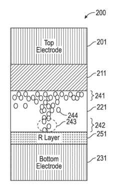
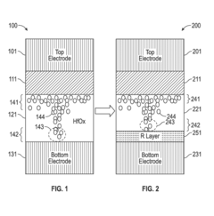
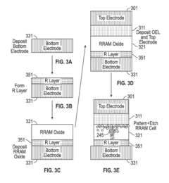
High retention resistive random access memory
PatentActiveUS20180309054A1
Innovation
- An RRAM stack is enhanced with an additional oxide thin film layer at the interface between the electrode and oxide, stabilizing oxygen vacancy migration and retention, allowing for reliable switching between high and low resistive states.
Resistance switching memory
PatentActiveUS8198620B2
Innovation
- A resistance switching memory with a stacked structure featuring a line-shaped top electrode, an insulating layer, and a resistance-switching material layer that covers the sidewall of the top electrode and contacts the lower electrode, utilizing an oxygen gettering metal layer to confine the switching area and prevent damage during fabrication.
ReRAM Standardization Efforts
Standardization efforts for Resistive Random Access Memory (ReRAM) have been gaining momentum as the technology matures and approaches wider commercial adoption. The JEDEC Solid State Technology Association has established working groups specifically focused on ReRAM standardization, addressing aspects such as interface protocols, reliability metrics, and testing methodologies. These efforts aim to create a unified framework that enables interoperability between ReRAM components from different manufacturers.
The IEEE has also contributed significantly to ReRAM standardization through its International Roadmap for Devices and Systems (IRDS), which includes ReRAM as a key emerging memory technology. Their standardization work focuses on establishing performance benchmarks and reliability requirements that align with industry needs across various application domains, from IoT devices to data center storage solutions.
Industry consortiums like SEMATECH and the Emerging Memory Devices Working Group have been instrumental in developing technical specifications for ReRAM integration with conventional CMOS processes. These specifications address critical parameters such as endurance requirements, retention characteristics, and power consumption profiles, providing manufacturers with clear guidelines for product development.
Patent analysis reveals that standardization efforts are increasingly reflected in intellectual property strategies, with major memory manufacturers filing patents specifically designed to align with emerging standards. Companies like Samsung, Micron, and Western Digital have been particularly active in developing IP portfolios that cover standard-compliant ReRAM implementations, indicating their commitment to standardized approaches.
The Global Semiconductor Alliance has established a ReRAM Interest Group that brings together device manufacturers, equipment suppliers, and end-users to coordinate standardization activities. This collaborative approach ensures that standards development incorporates perspectives from across the value chain, addressing both technical feasibility and market requirements.
China's standardization efforts deserve particular attention, with organizations like the China Electronics Standardization Institute actively developing national standards for ReRAM technology. These efforts are closely aligned with China's semiconductor self-sufficiency goals and may significantly influence global standardization dynamics as Chinese memory manufacturers expand their market presence.
Open-source initiatives are also emerging as complementary to formal standardization processes. Projects like OpenReRAM aim to develop standardized design libraries and verification methodologies that can accelerate ReRAM adoption while ensuring compatibility across different implementation approaches.
IP Strategy for ReRAM Development
The strategic management of intellectual property is crucial for companies developing Resistive RAM (ReRAM) technology. A comprehensive IP strategy must balance aggressive patent acquisition with defensive positioning to navigate this competitive landscape. Companies should prioritize filing patents for core ReRAM architectures, materials innovations, and manufacturing processes that offer distinct competitive advantages.
Cross-licensing agreements represent a valuable strategic approach, particularly for companies lacking comprehensive patent portfolios. These agreements can provide access to essential technologies while reducing litigation risks. For startups and smaller entities, strategic partnerships with established semiconductor manufacturers can offer both IP protection and manufacturing capabilities necessary for market entry.
Geographical considerations are equally important in ReRAM IP strategy. While the United States, China, and South Korea dominate patent filings, companies should consider strategic filings in emerging markets where ReRAM applications may experience rapid growth. This approach ensures protection in future high-value territories while managing filing costs effectively.
Freedom-to-operate (FTO) analyses should be conducted regularly to identify potential infringement risks before significant R&D investments. These analyses help companies navigate the complex patent landscape and avoid costly litigation. Additionally, maintaining trade secrets for certain manufacturing processes or material formulations can complement patent protection, especially for innovations difficult to reverse-engineer.
Open innovation models present another strategic option, where companies can participate in industry standards development or open-source initiatives to influence technology direction while maintaining proprietary advantages in specific areas. This balanced approach allows for ecosystem growth while preserving competitive differentiation.
Defensive publication represents a cost-effective strategy for innovations that may not warrant full patent protection. By publishing technical details, companies prevent competitors from patenting similar technologies while avoiding maintenance costs associated with formal patents.
Regular IP portfolio reviews are essential to align intellectual property assets with evolving business objectives. Companies should periodically evaluate their ReRAM patent portfolios, abandoning patents with diminishing value while reinforcing protection in emerging application areas such as neuromorphic computing or edge AI implementations.
Unlock deeper insights with Patsnap Eureka Quick Research — get a full tech report to explore trends and direct your research. Try now!
Generate Your Research Report Instantly with AI Agent
Supercharge your innovation with Patsnap Eureka AI Agent Platform!