

What are the Patent Challenges for Resistive RAM Technologies?
OCT 9, 20259 MIN READ
Generate Your Research Report Instantly with AI Agent
PatSnap Eureka helps you evaluate technical feasibility & market potential.
ReRAM Technology Background and Objectives
Resistive Random Access Memory (ReRAM) has emerged as a promising next-generation non-volatile memory technology over the past two decades. The evolution of ReRAM can be traced back to the early 2000s when researchers began exploring alternative memory technologies to overcome the scaling limitations of conventional flash memory. ReRAM's fundamental operating principle relies on the reversible resistance switching phenomenon in metal-oxide materials, where electrical resistance can be altered between high and low states through the application of appropriate voltage pulses.
The technology landscape has witnessed significant advancements in ReRAM development, progressing from basic proof-of-concept demonstrations to sophisticated multi-layer architectures. Early ReRAM devices faced challenges related to reliability, endurance, and uniformity, but continuous research efforts have led to substantial improvements in these areas. The technology has evolved from simple binary storage capabilities to multi-level cell configurations, enabling higher storage densities.
Current technical objectives in the ReRAM field focus on addressing several critical challenges. Patent landscapes reveal intensive research aimed at improving switching uniformity, reducing operating voltages, enhancing endurance beyond 10^9 cycles, and extending data retention periods to meet the 10-year industry standard. Additionally, significant efforts are directed toward developing scalable manufacturing processes compatible with existing CMOS fabrication techniques.
Material innovation represents another crucial aspect of ReRAM development. While early patents predominantly covered simple metal-oxide structures like HfO2 and TiO2, recent patent activities show increased interest in complex oxide systems, doped materials, and novel electrode configurations. These innovations aim to optimize the formation and dissolution of conductive filaments that underpin ReRAM's switching mechanism.
The integration of ReRAM into practical computing architectures constitutes a major technical objective evident in recent patent filings. Beyond traditional memory applications, patents increasingly explore ReRAM's potential for in-memory computing, neuromorphic applications, and edge AI implementations. These emerging applications leverage ReRAM's unique characteristics, including analog switching behavior, low power consumption, and non-volatility.
Patent challenges in the ReRAM domain have evolved alongside the technology itself. Early patents focused on basic switching mechanisms and device structures, while contemporary patent activities address more sophisticated aspects such as reliability enhancement techniques, novel programming algorithms, and system-level integration approaches. This evolution reflects the technology's maturation and its progression toward commercial viability.
Market Analysis for ReRAM Applications
The global market for Resistive Random Access Memory (ReRAM) technologies is experiencing significant growth, driven by increasing demand for high-performance, low-power memory solutions across multiple industries. Current market valuations place the ReRAM sector at approximately $310 million in 2023, with projections indicating a compound annual growth rate (CAGR) of 16% through 2030, potentially reaching $1.2 billion by the end of the decade.
The primary market segments for ReRAM applications can be categorized into four key areas: consumer electronics, automotive systems, industrial IoT, and enterprise storage solutions. Consumer electronics currently represents the largest market share at 42%, followed by enterprise storage at 28%, automotive applications at 18%, and industrial IoT at 12%. These proportions are expected to shift as automotive and IoT applications gain momentum in the coming years.
From a geographical perspective, North America leads ReRAM market adoption with 38% market share, followed by Asia-Pacific at 36%, Europe at 22%, and other regions accounting for the remaining 4%. China and South Korea are demonstrating particularly aggressive growth rates within the Asia-Pacific region, supported by substantial government investments in semiconductor technologies.
The demand drivers for ReRAM technologies are multifaceted. Edge computing applications require memory solutions with lower power consumption and faster write speeds than traditional flash memory, creating a significant opportunity for ReRAM deployment. The automotive sector's transition toward autonomous vehicles necessitates radiation-hardened, high-endurance memory that can withstand extreme operating conditions, another area where ReRAM excels.
Market adoption faces several challenges, including cost competitiveness against established technologies like NAND flash, which benefits from economies of scale. Current ReRAM solutions cost approximately 2.3 times more per gigabyte than equivalent NAND flash memory, though this gap is narrowing annually as manufacturing processes mature.
Patent landscape analysis reveals intensifying competition, with over 4,800 active patents related to ReRAM technologies globally. The most concentrated patent activity focuses on materials science innovations addressing retention and endurance limitations, with companies like Samsung, Micron, and Western Digital leading in patent filings.
Customer adoption surveys indicate that reliability and endurance remain the primary concerns for potential enterprise customers, with 68% citing these factors as critical decision criteria. Cost considerations rank second at 57%, while power efficiency and integration capabilities follow at 49% and 42% respectively.
Current ReRAM Patent Landscape and Barriers
The ReRAM patent landscape has become increasingly complex and crowded over the past decade, with major semiconductor companies, memory manufacturers, and research institutions aggressively filing patents to secure their positions in this emerging technology. Currently, the patent space is dominated by several key players including Samsung, Micron Technology, SK Hynix, Western Digital (through its SanDisk acquisition), and Intel, who collectively hold approximately 60% of all ReRAM-related patents.
A significant barrier in the ReRAM patent landscape is the fragmentation of intellectual property rights across multiple entities, creating a complex web of overlapping claims. This fragmentation has led to what industry analysts call a "patent thicket," where companies must navigate numerous licensing agreements or risk infringement litigation. For new entrants, this represents a substantial barrier to market entry without significant investment in licensing or legal resources.
The geographical distribution of patents reveals another challenge: while U.S. and Asian companies (particularly from South Korea, Japan, and increasingly China) hold the majority of patents, their focus areas differ significantly. U.S. patents tend to concentrate on architectural implementations and system integration, while Asian patents often focus on materials science innovations and manufacturing processes, creating regional imbalances in technology access.
Patent quality and enforceability present additional barriers. Many early ReRAM patents filed between 2005-2012 were broad in scope but lacked specific implementation details, leading to uncertainty about their enforceability. This has resulted in several high-profile patent disputes, most notably between Micron and Samsung in 2018, which have slowed industry-wide adoption and standardization efforts.
The patent landscape also reveals significant gaps in certain technical areas. While switching mechanisms and basic cell structures are well-covered by patents, areas such as reliability enhancement techniques, scaling solutions below 10nm, and 3D integration methods remain relatively underpatented, suggesting both opportunity and risk for companies developing these technologies.
Time-to-market pressures further complicate the patent situation. The average ReRAM patent application takes 3.2 years from filing to grant, during which time the technology landscape can change dramatically. This creates a situation where companies must make development decisions with incomplete knowledge of the eventual patent landscape they will face when bringing products to market.
Current Patent Strategies for ReRAM Development
01 Material composition challenges in ReRAM
Resistive RAM technologies face significant challenges related to material composition. The selection and optimization of materials for the resistive switching layer is critical for device performance. Challenges include finding materials with appropriate resistivity changes, stability over multiple switching cycles, and compatibility with existing semiconductor manufacturing processes. Researchers are exploring various oxide materials, metal alloys, and novel compounds to overcome these limitations and improve the reliability of ReRAM devices.- Material composition challenges in RRAM devices: Resistive RAM technologies face challenges related to the selection and optimization of materials used in the memory cells. The composition of the resistive switching layer, electrode materials, and interface properties significantly impact device performance, reliability, and endurance. Researchers are working to develop novel material combinations that can provide stable resistance states, lower power consumption, and improved retention characteristics while maintaining compatibility with standard semiconductor manufacturing processes.
- Scaling and integration issues: As RRAM technologies advance toward higher densities and smaller feature sizes, significant challenges emerge in maintaining performance while scaling down device dimensions. Integration with CMOS technology presents difficulties in terms of process compatibility, thermal budgets, and 3D stacking capabilities. These challenges include managing sneak current paths in crossbar arrays, developing suitable selector devices, and ensuring reliable operation at reduced cell sizes without compromising data retention or increasing variability.
- Reliability and endurance limitations: Resistive RAM technologies face significant challenges related to long-term reliability and endurance. These include resistance drift over time, cycle-to-cycle variability, and limited write endurance compared to conventional memory technologies. The physical mechanisms causing degradation, such as oxygen vacancy migration, filament formation instability, and electrode material diffusion, need to be better understood and controlled to improve device lifetime and maintain consistent performance over numerous programming cycles.
- Programming and operation optimization: Developing efficient programming schemes for RRAM devices presents significant challenges. These include optimizing the SET/RESET voltage pulses, managing the trade-off between programming speed and energy consumption, and implementing reliable multi-level cell operation. Controlling the current during the forming and SET operations is particularly challenging, as it affects the filament formation process and subsequent switching behavior. Advanced sensing circuits and programming algorithms are needed to ensure reliable operation while minimizing power consumption.
- Manufacturing and standardization barriers: The commercialization of RRAM technologies faces challenges related to manufacturing yield, process control, and industry standardization. Achieving consistent device characteristics across large wafers and between different production batches remains difficult. The lack of standardized testing methodologies and performance metrics makes it challenging to compare different RRAM technologies. Additionally, integrating RRAM into existing memory hierarchies requires addressing compatibility issues with memory controllers and developing appropriate interface standards.
02 Switching mechanism and reliability issues
A major patent challenge in ReRAM technology involves the switching mechanisms and reliability of the memory cells. The formation and rupture of conductive filaments that enable resistive switching can be inconsistent, leading to variability in performance. Patents in this area address issues such as retention time, endurance limitations, and read/write disturbances. Solutions include novel electrode designs, interface engineering, and controlling the filament formation process to achieve more predictable and stable switching behavior.Expand Specific Solutions03 Integration with CMOS technology
Integrating ReRAM with conventional CMOS technology presents significant patent challenges. These include developing compatible fabrication processes, addressing thermal budget constraints, and designing appropriate peripheral circuitry. The 3D integration of ReRAM cells to achieve higher density storage while maintaining CMOS compatibility is particularly challenging. Patents in this area focus on novel integration schemes, specialized interconnect structures, and process modifications that enable ReRAM to be manufactured alongside traditional semiconductor devices.Expand Specific Solutions04 Scaling and density optimization
As ReRAM technology advances, patents increasingly address challenges related to scaling and density optimization. Reducing the cell size while maintaining performance metrics is crucial for competing with other memory technologies. Challenges include minimizing sneak current paths in crossbar arrays, developing selector devices for high-density arrays, and ensuring reliable operation at smaller dimensions. Solutions involve novel cell architectures, improved selector devices, and advanced patterning techniques to achieve higher storage densities.Expand Specific Solutions05 Programming and sensing circuit design
Designing efficient programming and sensing circuits for ReRAM presents unique patent challenges. The variable resistance states in ReRAM cells require specialized circuits for accurate reading and writing operations. Patents in this area focus on developing precise current or voltage control mechanisms, addressing variability in switching thresholds, and creating energy-efficient programming schemes. Advanced sensing circuits that can reliably distinguish between resistance states while minimizing power consumption are also key areas of innovation in ReRAM patent landscapes.Expand Specific Solutions
Key Industry Players and Patent Holders
The Resistive RAM (ReRAM) technology landscape is currently in a transitional phase from research to early commercialization, with a global market projected to reach $4-5 billion by 2025. Major semiconductor players including Samsung, Micron, and TSMC are actively developing ReRAM solutions, while specialized companies like TetraMem and Ovonyx Memory Technology focus on niche applications. Patent challenges center around material stability, scaling limitations, and manufacturing integration. Research institutions such as ITRI, Fudan University, and Swiss Federal Institute of Technology collaborate with industry leaders to overcome technical barriers. The competitive landscape is characterized by strategic partnerships between memory manufacturers and foundries, with Asian companies (particularly from Taiwan and South Korea) demonstrating significant patent activity in addressing endurance, retention, and uniformity challenges.
Taiwan Semiconductor Manufacturing Co., Ltd.
Technical Solution: TSMC's ReRAM patent strategy focuses on manufacturing process integration and scalability challenges. As the world's leading semiconductor foundry, TSMC has developed specialized fabrication techniques for ReRAM that are compatible with their advanced logic processes, enabling embedded memory applications[2]. Their patents cover innovative electrode materials and interface engineering to improve switching uniformity and reduce forming voltages. TSMC has developed proprietary solutions for the critical challenge of ReRAM variability through process control innovations and specialized annealing techniques that stabilize oxygen vacancy distribution in metal oxide switching layers[5]. Their recent patents address integration challenges for ReRAM in advanced nodes below 10nm, including specialized etching processes, damage-free patterning techniques, and solutions for controlling thermal budgets during integration[9]. TSMC has also patented unique testing methodologies specific to ReRAM reliability assessment.
Strengths: Unparalleled manufacturing expertise and process control; ability to integrate ReRAM with advanced logic nodes; strong customer relationships for embedded memory applications. Weaknesses: Less control over end-product definition as a foundry; dependent on customer adoption; competing memory technologies in their manufacturing portfolio may create internal conflicts.
Samsung Electronics Co., Ltd.
Technical Solution: Samsung has developed a comprehensive ReRAM patent portfolio focusing on multi-level cell (MLC) capabilities and 3D integration. Their technology utilizes metal oxide-based switching materials (primarily HfOx and TaOx) with innovative electrode materials to enhance retention and endurance[1]. Samsung's cross-point array architecture enables high-density storage while addressing sneak path current issues through selector devices integrated with memory cells[3]. Their patents cover specialized forming processes that reduce operation voltages and improve uniformity across large arrays. Samsung has also developed unique solutions for the "voltage-time dilemma" in ReRAM by implementing adaptive programming schemes that optimize the trade-off between speed and reliability[5].
Strengths: Extensive manufacturing infrastructure allows for rapid commercialization; strong integration with existing CMOS processes; comprehensive IP portfolio covering materials, structures, and programming methods. Weaknesses: Faces challenges with variability in switching behavior across large arrays; reliability issues at advanced nodes below 20nm; competing internal technologies (V-NAND) may limit resource allocation.
Critical Patent Analysis for ReRAM Innovations
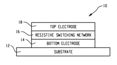
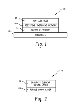
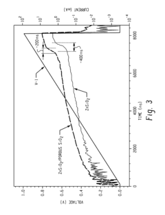
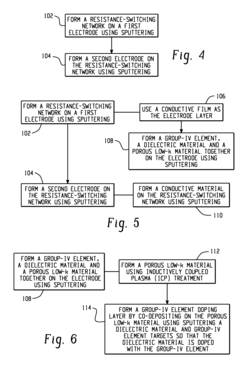
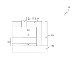
Resistive random-access memory (RRAM) with a low-k porous layer
PatentInactiveUS20150349251A1
Innovation
- Incorporating a porous low-k layer and a group-IV element doping layer in the resistance-switching network, where the porous low-k layer is prepared by inductively coupled plasma treatment and the group-IV element is doped into a dielectric material, enhances the switching speed and endurance by forming a multi-layer structure between the electrodes.
Structure and method for a complimentary resistive switching random access memory for high density application
PatentInactiveUS20130334486A1
Innovation
- A single stack complementary resistive switching (CRSRAM) structure is developed, which includes a stack of material layers with a defect engineering treatment process to generate oxygen vacancies, allowing for a simple structure with reduced fabrication costs and eliminating sneak path issues, featuring a single resistive state at lower voltages and dual states at higher voltages.
IP Risk Mitigation Strategies
In navigating the complex patent landscape surrounding Resistive RAM (ReRAM) technologies, companies must implement robust IP risk mitigation strategies to avoid costly litigation and ensure freedom to operate. A comprehensive approach begins with thorough patent landscaping, which involves systematic mapping of existing patents in the ReRAM domain. This process identifies key patent holders, technology clusters, and potential white spaces for innovation, providing strategic intelligence for R&D direction and business decisions.
Design-around strategies represent another critical component of risk mitigation. By analyzing competitors' patent claims in detail, companies can develop alternative technical solutions that achieve similar functionality while avoiding infringement. This approach often leads to innovative solutions that may themselves be patentable, creating defensive IP assets while minimizing legal exposure.
Proactive patent portfolio development serves as both shield and sword in the competitive ReRAM market. Companies should prioritize filing patents that protect core technologies while also developing strategic defensive patents that can serve as bargaining chips in potential disputes. Particular attention should be paid to method patents covering manufacturing processes, which are often more defensible than device patents in the semiconductor industry.
Cross-licensing agreements offer a collaborative approach to risk mitigation. By establishing mutually beneficial arrangements with key patent holders, companies can secure freedom to operate while reducing litigation risk. These agreements are particularly valuable in the ReRAM ecosystem, where complementary technologies often require integration from multiple sources.
Prior art monitoring represents an ongoing vigilance strategy. By systematically tracking new patent applications in the ReRAM field, companies can file timely oppositions or provide evidence of prior art when appropriate. This proactive approach can prevent competitors from obtaining overly broad patents that might later become litigation threats.
For startups and smaller entities entering the ReRAM space, patent pooling arrangements provide access to essential IP without prohibitive licensing costs. These collaborative structures distribute risk across multiple participants while ensuring compliance with patent requirements, enabling innovation without excessive legal exposure.
Finally, companies should establish clear internal protocols for IP risk assessment, including regular freedom-to-operate analyses before major product launches or technology implementations. These protocols should include documentation practices that create evidence trails for independent development, potentially providing invaluable defense in future disputes.
Cross-Licensing and Collaboration Frameworks
In the complex landscape of Resistive RAM (ReRAM) technology development, cross-licensing and collaboration frameworks have emerged as critical strategies for navigating patent challenges. The fragmented nature of ReRAM intellectual property across multiple organizations necessitates structured approaches to technology sharing. Major semiconductor companies including Samsung, Micron, and Western Digital have established bilateral cross-licensing agreements specifically for ReRAM technologies, allowing mutual access to essential patents while maintaining competitive differentiation in implementation.
Industry consortia represent another significant collaboration model, with organizations like IMEC and the Storage Networking Industry Association (SNIA) creating patent pools where members contribute intellectual property under standardized licensing terms. These arrangements have proven particularly valuable for addressing fundamental material science challenges in ReRAM development, such as filament formation mechanisms and electrode material optimization.
University-industry partnerships constitute a third framework, exemplified by Stanford University's collaboration with memory manufacturers to develop novel switching materials while establishing clear IP ownership protocols. These partnerships typically involve tiered licensing structures where academic institutions retain publication rights while industry partners secure commercialization pathways.
The semiconductor industry has also developed specialized patent clearinghouses for memory technologies, creating marketplace mechanisms where ReRAM patents can be licensed, sold, or exchanged with standardized valuation methodologies. This approach has helped smaller innovators monetize their intellectual property while giving established manufacturers access to specialized solutions for specific technical challenges.
Open innovation initiatives represent an emerging trend, with companies like IBM and Intel selectively releasing non-core ReRAM patents to stimulate ecosystem development. These initiatives typically maintain proprietary protection for key competitive advantages while opening peripheral technologies to broader development communities.
Regional collaboration frameworks have also emerged, particularly in East Asia where government-sponsored programs in Japan, South Korea, and China facilitate cross-border technology transfer for ReRAM development. These frameworks often include standardized dispute resolution mechanisms and harmonized patent enforcement protocols to reduce litigation risks.
The evolution of these collaboration models reflects the recognition that ReRAM commercialization requires complementary expertise across materials science, device physics, circuit design, and manufacturing processes—competencies rarely found within a single organization. As ReRAM moves toward mainstream adoption, these frameworks will likely become increasingly sophisticated, potentially incorporating blockchain-based smart contracts for automated licensing compliance and royalty distribution.
Unlock deeper insights with PatSnap Eureka Quick Research — get a full tech report to explore trends and direct your research. Try now!
Generate Your Research Report Instantly with AI Agent
Supercharge your innovation with PatSnap Eureka AI Agent Platform!