

Defining Parameters in Resistive RAM Technological Breakthroughs
OCT 9, 20259 MIN READ
Generate Your Research Report Instantly with AI Agent
PatSnap Eureka helps you evaluate technical feasibility & market potential.
ReRAM Technology Evolution and Objectives
Resistive Random Access Memory (ReRAM) has emerged as a promising non-volatile memory technology over the past two decades, evolving from theoretical concepts to practical implementations. The technology leverages the resistance switching phenomenon observed in certain metal oxides and other materials, where electrical resistance can be altered through the application of voltage, creating stable states that represent binary data. This fundamental principle has positioned ReRAM as a potential successor to conventional memory technologies like NAND flash and DRAM.
The evolution of ReRAM technology can be traced back to the early 2000s when researchers began exploring resistance switching mechanisms in various material systems. Initial demonstrations focused on simple metal-insulator-metal structures, which gradually evolved into more sophisticated architectures incorporating advanced materials and fabrication techniques. The period between 2010 and 2015 marked significant advancements in understanding the underlying physics of filamentary and interface-type switching mechanisms, leading to improved device reliability and performance.
Recent technological breakthroughs have centered on addressing critical parameters that influence ReRAM operation, including switching voltage, current compliance, retention time, endurance, and read/write speeds. These parameters are fundamentally interconnected, creating complex optimization challenges that researchers continue to navigate. For instance, reducing switching voltage often compromises retention time, while enhancing endurance may impact switching speed or power consumption.
The industry has witnessed a gradual shift from academic research to commercial development, with companies like Crossbar, Weebit Nano, and established semiconductor manufacturers investing in ReRAM technology. This transition has emphasized the importance of defining standardized parameters and testing methodologies to facilitate technology comparison and integration into existing semiconductor ecosystems.
Current technological objectives focus on several key areas: reducing operating voltage to below 1V for compatibility with advanced CMOS processes; improving endurance beyond 10^12 cycles to compete with DRAM; enhancing retention time at elevated temperatures (typically >10 years at 85°C); and increasing switching speed to sub-nanosecond range. Additionally, there is growing emphasis on multi-level cell capabilities to increase storage density and neuromorphic computing applications that leverage the analog nature of resistance changes.
The trajectory of ReRAM development is increasingly influenced by emerging applications in edge computing, Internet of Things (IoT), and artificial intelligence, which demand memory solutions with unique combinations of power efficiency, speed, and reliability. As these application spaces evolve, the definition and prioritization of critical ReRAM parameters continue to be refined, guiding research efforts toward commercially viable solutions that can address specific market needs.
Market Analysis for ReRAM Applications
The global ReRAM (Resistive Random Access Memory) market is experiencing significant growth, with projections indicating expansion from $1.2 billion in 2023 to approximately $4.6 billion by 2028, representing a compound annual growth rate of 30.8%. This remarkable growth trajectory is primarily driven by increasing demand for high-performance, energy-efficient memory solutions across multiple sectors.
The consumer electronics segment currently dominates ReRAM applications, accounting for nearly 40% of market share. Smartphones, tablets, and wearable devices manufacturers are increasingly adopting ReRAM technology due to its low power consumption characteristics and faster write speeds compared to traditional flash memory. Major smartphone manufacturers have begun incorporating ReRAM components in their flagship devices, signaling growing market acceptance.
Enterprise storage systems represent the second-largest application segment, with approximately 25% market share. Data centers and cloud service providers are exploring ReRAM solutions to address the limitations of current memory hierarchies, particularly for applications requiring high-speed data processing with minimal energy consumption. The technology's non-volatile nature combined with DRAM-like performance makes it particularly attractive for these use cases.
Automotive applications are emerging as the fastest-growing segment, with projected growth rates exceeding 35% annually through 2028. Advanced driver-assistance systems (ADAS) and autonomous vehicles require memory solutions capable of operating reliably in extreme conditions while processing vast amounts of sensor data with minimal latency. ReRAM's radiation hardness and temperature stability provide significant advantages in this demanding environment.
The industrial IoT sector presents substantial growth opportunities, particularly for edge computing applications where power efficiency is paramount. Market analysis indicates that ReRAM-based edge devices can reduce power consumption by up to 70% compared to flash-based alternatives, extending battery life and enabling deployment in remote locations.
Geographically, North America leads ReRAM adoption with approximately 38% market share, followed by Asia-Pacific at 35%. The European market accounts for 20%, with particularly strong growth in automotive applications. China has emerged as a critical manufacturing hub, with significant investments in domestic ReRAM production capabilities to reduce dependency on imported memory technologies.
Market challenges include competition from alternative emerging memory technologies such as MRAM and PCM, as well as the established infrastructure supporting traditional memory solutions. Additionally, standardization issues and manufacturing scalability remain obstacles to wider adoption, though recent technological breakthroughs in defining critical parameters for ReRAM fabrication are addressing these limitations.
Current ReRAM Parameter Challenges
Resistive RAM (ReRAM) technology faces several critical parameter challenges that currently limit its widespread commercial adoption. The primary challenge lies in achieving consistent switching parameters across devices and over multiple operating cycles. Resistance states in ReRAM cells often exhibit significant variability, with resistance values fluctuating by up to 20-30% between cycles, making reliable multi-bit storage particularly difficult to implement in practical applications.
The endurance parameter presents another substantial hurdle, with current ReRAM devices typically achieving 10^6 to 10^9 write cycles before failure. While this exceeds flash memory capabilities, it falls short of DRAM and SRAM performance metrics required for universal memory applications. The endurance degradation mechanisms remain incompletely understood, complicating efforts to engineer more durable solutions.
Retention time parameters show concerning temperature dependence, with data retention periods decreasing exponentially as operating temperatures increase. At elevated temperatures (>85°C), some ReRAM devices experience accelerated data loss, raising reliability concerns for automotive and industrial applications where extended temperature ranges are common requirements.
Switching speed parameters exhibit asymmetry between SET and RESET operations, with typical SET operations requiring 10-50ns while RESET operations can be completed in 5-20ns. This asymmetry complicates driver circuit design and creates timing challenges in high-speed memory applications. Additionally, the energy consumption during switching operations remains higher than ideal, with current devices requiring 0.1-10 pJ per switching event.
The scaling parameter presents a fundamental physics challenge, as ReRAM cells below certain dimensions (~10nm) demonstrate increased variability and reduced reliability. This scaling limitation threatens the technology's long-term competitiveness against other emerging memory technologies with potentially better scaling characteristics.
Material interface parameters contribute significantly to device performance variability. The electrode-oxide interface characteristics can change during fabrication or operation, affecting critical parameters like forming voltage, SET/RESET voltages, and resistance states. Current fabrication processes struggle to maintain consistent interface properties across large arrays.
Integration parameters with CMOS technology present additional challenges, particularly regarding the thermal budget compatibility and potential contamination issues. The high temperatures sometimes required for ReRAM fabrication (>400°C) can adversely affect underlying CMOS components, limiting back-end-of-line integration options.
The read disturb parameter remains problematic, as repeated read operations at sub-threshold voltages can gradually shift resistance states, eventually causing data corruption. This effect becomes more pronounced as cell dimensions decrease, creating a fundamental reliability challenge for high-density ReRAM implementations.
Parameter Optimization Approaches
01 Material composition and structure for RRAM devices
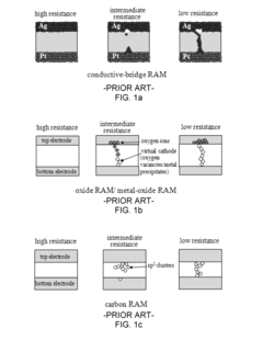
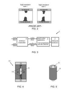
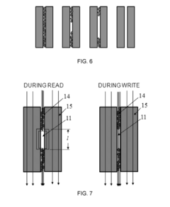
Resistive RAM devices utilize specific material compositions and structures to achieve desired switching characteristics. These materials often include metal oxides, chalcogenides, or perovskites that exhibit resistive switching behavior. The structure typically consists of a switching layer sandwiched between two electrodes. The composition and structure significantly influence parameters such as switching voltage, resistance ratio, endurance, and retention time of the RRAM devices.- Material composition and structure for RRAM devices: The material composition and structure of resistive RAM devices significantly impact their performance. Various materials such as metal oxides, chalcogenides, and perovskites are used as the resistive switching layer. The structure typically includes a top electrode, resistive switching layer, and bottom electrode. The interface between these layers plays a crucial role in determining the switching behavior. Optimizing the material composition and structure can lead to improved switching characteristics, endurance, and retention time.
- Switching mechanisms and operational parameters: Resistive RAM operates based on different switching mechanisms including filamentary conduction, interface-type switching, and valence change. Key operational parameters include SET/RESET voltages, switching current, resistance ratio between high and low resistance states, and switching speed. These parameters determine the performance of RRAM devices in terms of power consumption, reliability, and speed. Controlling these parameters through proper device design and operation conditions is essential for optimal RRAM performance.
- Reliability and endurance characteristics: Reliability and endurance are critical parameters for resistive RAM devices. These include retention time (how long the device can maintain its state), endurance (number of write/erase cycles), and variability (consistency of performance across cycles and between devices). Factors affecting these characteristics include operating temperature, stress conditions, and material degradation mechanisms. Various techniques such as pulse engineering, doping, and interface engineering are employed to enhance the reliability and endurance of RRAM devices.
- Integration and fabrication techniques: Integration of resistive RAM with conventional CMOS technology and fabrication techniques significantly impact device parameters. Key considerations include process compatibility, thermal budget, scaling potential, and 3D integration capabilities. Advanced fabrication techniques such as atomic layer deposition, reactive sputtering, and precise control of layer thicknesses are employed to achieve desired device characteristics. The choice of electrode materials and deposition methods also affects the interface properties and overall device performance.
- Circuit design and programming strategies: Circuit design and programming strategies are essential for optimizing resistive RAM performance. These include sensing circuits for reading the resistance state, programming circuits for applying appropriate voltage/current pulses, and reference schemes for reliable state discrimination. Various programming strategies such as compliance current control, pulse width modulation, and multi-level cell programming are employed to achieve desired switching behavior. Advanced circuit techniques are also used to mitigate issues like sneak path currents in crossbar arrays and to improve overall system performance.
02 Operational parameters and programming methods
RRAM devices require specific operational parameters for reliable performance, including programming voltage, current compliance, pulse width, and read voltage. These parameters determine how the device switches between high and low resistance states. Programming methods may involve voltage sweeps, current pulses, or other techniques to control the formation and rupture of conductive filaments within the switching layer, affecting the overall performance and reliability of the memory cell.Expand Specific Solutions03 Fabrication techniques and process parameters
Fabrication of RRAM devices involves various process parameters that significantly impact device performance. These include deposition methods (such as sputtering, atomic layer deposition, or chemical vapor deposition), annealing temperatures, layer thicknesses, and electrode materials. Controlling these parameters during manufacturing is crucial for achieving consistent device characteristics, high yield, and reliability in resistive memory arrays.Expand Specific Solutions04 Reliability and endurance characteristics
Reliability parameters for RRAM include endurance (number of write/erase cycles), data retention time, resistance drift, and failure mechanisms. These parameters are influenced by operating conditions such as temperature, voltage stress, and cycling frequency. Understanding and optimizing these reliability factors is essential for ensuring long-term stability and performance of RRAM devices in various applications, particularly in environments with demanding requirements.Expand Specific Solutions05 Integration and scaling parameters
Integration of RRAM into memory arrays and systems requires consideration of scaling parameters, including cell size, density, cross-talk between adjacent cells, and compatibility with CMOS processes. As device dimensions shrink, parameters such as operating voltage, power consumption, and switching speed become increasingly important. Advanced architectures like crossbar arrays and 3D stacking introduce additional parameters related to interconnects, selector devices, and addressing schemes that affect overall memory performance.Expand Specific Solutions
Leading ReRAM Industry Players
The Resistive RAM (ReRAM) technology landscape is currently in a growth phase, with the market expected to expand significantly as this non-volatile memory solution addresses limitations of traditional memory technologies. The competitive field features diverse players across multiple regions, with particularly strong representation from Asian institutions. Academic research centers like Peking University, Fudan University, and GIST are advancing fundamental breakthroughs, while established semiconductor giants including Samsung, SK Hynix, and TSMC provide manufacturing expertise and scale. Specialized ReRAM-focused companies such as CrossBar and Weebit Nano are driving commercial innovation. The technology is approaching commercial maturity with several companies demonstrating working prototypes, though challenges in manufacturing consistency, endurance, and integration with existing semiconductor processes remain before widespread adoption occurs.
Samsung Electronics Co., Ltd.
Technical Solution: Samsung has developed advanced HfO2-based ReRAM technology with precisely defined parameter windows for optimal performance. Their approach incorporates a bilayer structure with engineered oxygen concentration gradients between layers to control filament formation dynamics. Samsung's ReRAM cells operate with SET voltages of 1.0-1.5V and RESET voltages of 0.7-1.2V, carefully optimized to balance power consumption and reliability. The company has defined critical current compliance parameters (typically 50-200μA) that prevent over-programming while ensuring stable resistance states. Their technology features a proprietary electrode interface engineering method that reduces variability in resistance states to <20% across billions of cells. Samsung has demonstrated successful integration of ReRAM arrays with their advanced logic processes at 28nm node, achieving read latencies below 50ns and write latencies below 100ns. The company has also defined specific pulse width parameters (10-50ns) that optimize the energy-delay product while maintaining reliability metrics including 10-year retention at 85°C and endurance exceeding 10^9 cycles.
Strengths: Extensive manufacturing infrastructure and integration capabilities with existing memory technologies; demonstrated high endurance exceeding 10^9 cycles. Weaknesses: Higher current operation compared to some competitors, potentially limiting application in ultra-low power scenarios; complex bilayer structure may increase manufacturing challenges.
CrossBar, Inc.
Technical Solution: CrossBar has pioneered a unique approach to ReRAM technology with their patented 1TnR (one transistor driving multiple ReRAM cells) architecture. Their solution utilizes a non-filamentary switching mechanism based on silver-doped silicon-based switching material that forms a conductive path between electrodes when voltage is applied. This approach enables CrossBar to achieve high density memory arrays with excellent retention characteristics (>10 years at 85°C) and endurance exceeding 10^6 cycles. The company has defined critical parameters including SET/RESET voltages (typically 1-3V), switching current (sub-μA range), and read voltage (<0.5V) that optimize power consumption while maintaining reliability. Their cell structure incorporates engineered oxygen vacancies and defect management to control filament formation and dissolution processes, resulting in more predictable switching behavior and reduced variability between cells.
Strengths: Superior scalability down to 10nm nodes with excellent retention and endurance characteristics; non-filamentary approach reduces variability issues common in filamentary ReRAM. Weaknesses: Requires specialized materials integration that may increase manufacturing complexity; still faces challenges in multi-level cell implementation for higher density applications.
Critical Patents in ReRAM Parameter Design
Method for determining a manufacturing parameter of a resistive random access memory cell
PatentActiveUS20220336017A1
Innovation
- A method to determine optimal manufacturing parameters for resistive memory cells by establishing relationships between initial resistance, high resistance state resistance, and programming window, allowing for adjustments to enhance the programming window, involving the use of reference memory cells with varying parameters such as electrode thickness and oxygen proportion in silicon oxide layers.
Resistive random-access memory cells
PatentActiveUS20160196874A1
Innovation
- The introduction of an electrically-conductive component within the RRAM cell structure, which allows for programmable cell states by varying the resistance of the conductive path and insulating matrix, enabling effective differentiation of high-resistance states and reducing sneak-path currents without destructive read operations.
Materials Science Advancements for ReRAM
The evolution of Resistive Random Access Memory (ReRAM) technology has been significantly influenced by breakthroughs in materials science. Traditional ReRAM structures relied primarily on metal oxides such as HfO2, TiO2, and Ta2O5, which demonstrated basic switching capabilities but suffered from reliability issues and performance limitations.
Recent advancements in material engineering have introduced novel compounds and composite structures that dramatically enhance ReRAM performance parameters. Two-dimensional (2D) materials, particularly transition metal dichalcogenides (TMDs) like MoS2 and WSe2, have emerged as promising candidates for ReRAM switching layers due to their atomically thin nature and tunable electronic properties.
Researchers have developed innovative heterostructure configurations combining different materials to optimize specific performance metrics. For instance, the integration of graphene electrodes with metal oxide switching layers has shown remarkable improvements in switching speed and energy efficiency. These hybrid structures leverage the high conductivity of graphene while maintaining the reliable resistive switching characteristics of metal oxides.
Doping strategies have revolutionized the control of defect engineering in ReRAM materials. Precise introduction of dopants such as nitrogen in HfO2 or aluminum in TiO2 has enabled fine-tuning of oxygen vacancy concentration, which directly influences switching behavior and retention characteristics. This approach has led to devices with significantly improved endurance, exceeding 10^9 switching cycles in laboratory demonstrations.
Interface engineering represents another critical advancement area, where researchers have developed techniques to control the formation and migration of conductive filaments at material interfaces. Atomic Layer Deposition (ALD) and Pulsed Laser Deposition (PLD) methods have enabled precise control over interface properties at the nanoscale, resulting in more predictable and stable switching behavior.
Emerging materials such as perovskites and metal-organic frameworks (MOFs) are expanding the possibilities for ReRAM applications. These materials offer unique properties including tunable bandgaps, controllable ion migration pathways, and compatibility with flexible substrates. Particularly noteworthy is the development of halide perovskites for ReRAM, which has demonstrated multi-level storage capabilities with remarkably low power consumption.
The integration of phase-change materials with traditional ReRAM structures has created hybrid devices that combine the advantages of both technologies. These composite systems exhibit enhanced switching ratios and improved retention characteristics while maintaining the fast switching speeds characteristic of ReRAM technology.
Integration Strategies with Existing Memory Technologies
The integration of Resistive RAM (ReRAM) with existing memory technologies represents a critical pathway for its commercial adoption and market penetration. Current memory ecosystems are dominated by established technologies such as DRAM, NAND Flash, and SRAM, each serving specific roles in the memory hierarchy. ReRAM's successful deployment depends significantly on how seamlessly it can be integrated with these incumbent technologies.
Hybrid memory systems combining ReRAM with conventional memories offer promising solutions to address performance gaps in current architectures. For instance, ReRAM-DRAM hybrid configurations leverage DRAM's high speed for frequently accessed data while utilizing ReRAM's non-volatility and density for less frequently accessed information. This complementary approach optimizes both performance and power consumption across diverse workloads.
Interface compatibility presents a significant integration challenge. ReRAM must conform to established memory protocols and bus architectures to minimize adoption barriers. Industry efforts have focused on developing ReRAM modules that adhere to standard interfaces like DDR4/5 or PCIe, enabling drop-in replacement capabilities without requiring extensive system redesigns. This compatibility-focused approach reduces integration costs and accelerates market acceptance.
Manufacturing integration represents another crucial dimension. Leading semiconductor companies have invested in developing process technologies that allow ReRAM fabrication alongside conventional memory components. Advanced 3D integration techniques, including through-silicon vias (TSVs) and monolithic 3D integration, enable the vertical stacking of ReRAM with existing memory technologies, maximizing density while minimizing interconnect delays.
Software stack adaptation constitutes an equally important integration consideration. Memory controllers, operating systems, and applications require modifications to effectively utilize ReRAM's unique characteristics. Intelligent memory management algorithms that dynamically allocate data between ReRAM and conventional memories based on access patterns, persistence requirements, and energy constraints are being developed to maximize system performance.
Several commercial products have demonstrated successful integration strategies. Intel's Optane DC Persistent Memory modules, though based on 3D XPoint rather than pure ReRAM, established a precedent for integrating non-volatile memory technologies alongside DRAM in data center environments. Similarly, embedded systems manufacturers have begun incorporating ReRAM as NOR Flash replacements in microcontrollers, leveraging existing peripheral interfaces while delivering improved performance and endurance.
Unlock deeper insights with PatSnap Eureka Quick Research — get a full tech report to explore trends and direct your research. Try now!
Generate Your Research Report Instantly with AI Agent
Supercharge your innovation with PatSnap Eureka AI Agent Platform!