Analysis of Resistive RAM in New Semiconductor Standards
OCT 9, 202510 MIN READ
Generate Your Research Report Instantly with AI Agent
Patsnap Eureka helps you evaluate technical feasibility & market potential.
RRAM Technology Evolution and Objectives
Resistive Random Access Memory (RRAM) has emerged as a promising technology in the evolving landscape of non-volatile memory solutions. Since its conceptualization in the early 2000s, RRAM has progressed from theoretical research to practical implementation, driven by the increasing demand for high-density, low-power memory solutions in various electronic applications. The technology leverages resistance switching phenomena in metal-oxide materials to store information, offering advantages in terms of scalability, power consumption, and integration potential.
The evolution of RRAM technology has been marked by significant milestones in material science and fabrication techniques. Initial research focused on understanding the fundamental mechanisms of resistive switching in various oxide materials such as HfO2, TiO2, and Ta2O5. By the mid-2010s, researchers had developed more sophisticated models explaining the formation and rupture of conductive filaments within these materials, leading to improved device reliability and performance.
Recent advancements have shifted toward optimizing RRAM for specific applications and addressing key challenges such as endurance, retention, and variability. The integration of RRAM with conventional CMOS technology has been a critical focus area, enabling its incorporation into existing semiconductor manufacturing processes. This compatibility has positioned RRAM as a viable candidate for next-generation memory solutions in an increasingly data-centric computing environment.
The primary objective of RRAM development within new semiconductor standards is to establish it as a mainstream memory technology capable of addressing the limitations of current solutions. Specifically, RRAM aims to bridge the performance gap between high-speed, volatile memories (DRAM) and high-density, non-volatile storage (NAND Flash). This "storage-class memory" would enable new computing architectures and applications that require both persistence and high performance.
Technical objectives for RRAM include achieving sub-10nm scalability while maintaining reliable switching characteristics, reducing operating voltages to enhance energy efficiency, and improving endurance beyond 10^12 cycles to compete with existing memory technologies. Additionally, researchers are working to enhance multi-level cell capabilities, allowing each RRAM cell to store multiple bits and thereby increasing memory density.
From a standardization perspective, the semiconductor industry is working to establish consistent testing methodologies, reliability criteria, and interface protocols for RRAM technology. Organizations such as JEDEC and IEEE are developing standards that will facilitate broader adoption of RRAM in commercial applications, ensuring interoperability and reliability across different implementations.
The trajectory of RRAM evolution points toward its potential integration in emerging computing paradigms such as neuromorphic computing and in-memory processing. These applications leverage RRAM's analog switching characteristics to perform computational tasks directly within memory arrays, potentially revolutionizing the traditional von Neumann computing architecture and addressing the growing challenges of data movement in modern computing systems.
Market Analysis for RRAM Applications
The global market for Resistive Random Access Memory (RRAM) is experiencing significant growth, driven by increasing demand for high-performance, energy-efficient memory solutions across various industries. Current market valuations place the RRAM sector at approximately $310 million in 2023, with projections indicating a compound annual growth rate (CAGR) of 16.2% through 2030, potentially reaching $950 million by the end of the forecast period.
The consumer electronics segment currently dominates RRAM applications, accounting for roughly 38% of market share. This dominance stems from RRAM's advantages in mobile devices, wearables, and smart home products where power efficiency and fast access times are critical performance factors. The non-volatile nature of RRAM provides substantial battery life improvements compared to traditional memory technologies.
Enterprise storage systems represent the second-largest application segment at 27% market share, where RRAM's high endurance and reliability characteristics make it particularly valuable for data centers and cloud infrastructure. The technology's ability to maintain data integrity during power loss events provides significant operational advantages in these environments.
Automotive applications are emerging as the fastest-growing segment with a projected CAGR of 22.5% through 2030. This growth is primarily driven by advanced driver-assistance systems (ADAS) and autonomous vehicle development, where RRAM's radiation hardness and temperature stability provide critical advantages over conventional memory technologies.
Industrial IoT applications constitute approximately 18% of the current market, with implementations focusing on edge computing devices and sensor networks where power constraints are significant considerations. The remaining market share is distributed across medical devices, aerospace, and military applications, each leveraging RRAM's unique performance characteristics.
Geographically, North America leads RRAM adoption with 42% market share, followed by Asia-Pacific at 36%, Europe at 18%, and the rest of the world at 4%. However, the Asia-Pacific region is expected to demonstrate the highest growth rate over the next five years due to expanding semiconductor manufacturing capabilities and increasing electronic device production.
Key market challenges include cost competitiveness against established memory technologies and manufacturing scalability issues. Despite these challenges, the integration of RRAM into emerging computing architectures, particularly neuromorphic computing systems and AI accelerators, presents substantial growth opportunities. Industry analysts predict that neuromorphic applications alone could contribute an additional $120 million to the RRAM market by 2028.
RRAM Development Status and Technical Barriers
Resistive RAM (RRAM) technology has emerged as a promising candidate for next-generation non-volatile memory solutions, offering advantages in scalability, power consumption, and integration capabilities. However, the global development status reveals significant disparities in technological maturity and adoption rates across different regions and applications.
In the United States, major semiconductor companies like Intel, Micron, and Western Digital have established substantial RRAM research programs, focusing primarily on integration with conventional CMOS processes. These efforts have yielded functional prototypes with densities approaching 16Gb, though commercial deployment remains limited to specialized applications.
Asian manufacturers, particularly in South Korea, Japan, and Taiwan, have demonstrated remarkable progress in RRAM fabrication techniques. Companies such as Samsung, SK Hynix, and TSMC have invested heavily in manufacturing infrastructure capable of supporting RRAM production at competitive price points, positioning themselves advantageously for future market expansion.
European research institutions maintain leadership in fundamental materials science related to RRAM, with consortia like IMEC and Fraunhofer developing novel switching materials and characterization methodologies. However, translation of these scientific advances into commercial products has progressed more slowly compared to Asian counterparts.
Despite promising developments, RRAM technology faces several critical technical barriers that impede widespread adoption. Foremost among these is the challenge of retention reliability, with current implementations struggling to maintain data integrity beyond 10 years at elevated temperatures. This limitation particularly affects automotive and industrial applications where extended temperature ranges are required.
Endurance capabilities present another significant hurdle, with most RRAM cells demonstrating write cycle limitations of 10^6 to 10^8 operations before performance degradation. While sufficient for storage applications, this falls short of requirements for working memory or in-memory computing scenarios that demand 10^12 cycles or more.
Variability in switching behavior represents perhaps the most fundamental challenge, manifesting as inconsistent resistance states between cycles and across different cells. This variability complicates multi-level cell implementations and necessitates complex error correction schemes that increase system overhead and power consumption.
Manufacturing integration presents additional complications, particularly regarding compatibility with back-end-of-line (BEOL) processes in standard semiconductor fabrication. Temperature constraints during integration often compromise material properties, resulting in performance degradation compared to laboratory demonstrations.
The scaling trajectory of RRAM also faces increasing challenges below 20nm node, where quantum effects and material constraints begin to dominate device physics. Innovative materials and cell architectures will be essential to maintain the theoretical density advantages of RRAM technology at advanced nodes.
Current RRAM Implementation Approaches
01 Materials and structures for RRAM devices
Resistive Random Access Memory (RRAM) devices utilize specific materials and structures to enable resistive switching behavior. These typically include metal oxides like HfO2, TiO2, or Ta2O5 as the switching layer sandwiched between two electrodes. The structure may incorporate additional layers such as barrier layers or doping elements to enhance performance. The specific arrangement of these materials significantly impacts the device's switching characteristics, endurance, and retention properties.- Resistive RAM device structures: Resistive RAM (RRAM) devices are constructed with specific structural configurations to optimize performance. These structures typically include a resistive switching layer sandwiched between two electrodes. Various materials can be used for the resistive layer, including metal oxides, chalcogenides, and perovskites. The electrode materials and their interfaces with the resistive layer play crucial roles in determining switching characteristics. Advanced structures may incorporate additional layers for improved stability, retention, and endurance.
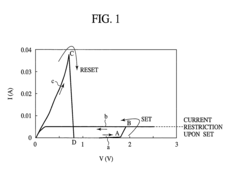
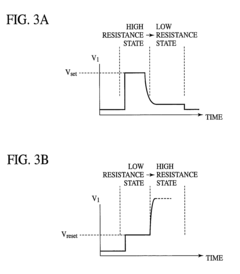
- Resistive switching mechanisms: The operation of resistive RAM relies on various switching mechanisms that enable transitions between high and low resistance states. These mechanisms include filamentary conduction, where conductive filaments form and rupture within the resistive layer, and interface-type switching, where resistance changes occur at the electrode-oxide interfaces. The switching can be controlled by voltage polarity (bipolar switching) or voltage amplitude (unipolar switching). Understanding these mechanisms is essential for designing reliable RRAM devices with consistent performance characteristics.
- Materials for resistive RAM: Material selection is critical for resistive RAM performance. Common materials for the resistive switching layer include transition metal oxides (such as HfOx, TaOx, and TiOx), chalcogenides (like GeSbTe), and complex oxides. Electrode materials range from noble metals (Pt, Au) to reactive metals (Ti, Ta) and conductive nitrides (TiN, TaN). Doping the switching layer with specific elements can enhance switching characteristics, while interface engineering between the electrodes and switching layer can improve device reliability and performance.
- Integration and fabrication techniques: Fabrication of resistive RAM involves various integration techniques compatible with conventional semiconductor processing. These include physical vapor deposition, atomic layer deposition, and chemical vapor deposition for thin film growth. Patterning techniques such as lithography and etching are used to define device structures. Integration challenges include ensuring compatibility with CMOS processes, minimizing thermal budgets, and developing 3D stacking approaches for high-density memory arrays. Advanced fabrication methods focus on controlling film stoichiometry, interface quality, and defect concentrations.
- Circuit design and operation: Circuit design for resistive RAM encompasses sensing schemes, programming algorithms, and array architectures. Sensing circuits must accurately distinguish between high and low resistance states while minimizing read disturbance. Programming circuits deliver precise voltage or current pulses to set and reset the memory cells. Array architectures address issues like sneak path currents through selector devices or crossbar configurations. Advanced circuit techniques include multi-level cell operation, error correction, and wear-leveling algorithms to extend device lifetime and reliability.
02 Switching mechanisms in RRAM
RRAM operates based on resistive switching mechanisms where the resistance of the memory cell can be altered between high and low states. This switching behavior typically occurs through the formation and rupture of conductive filaments within the switching layer. The filaments may consist of oxygen vacancies or metal ions that migrate under an applied electric field. Understanding and controlling these mechanisms is crucial for improving device reliability, reducing variability, and enhancing overall performance.Expand Specific Solutions03 Integration and fabrication techniques
The fabrication of RRAM devices involves various integration techniques to ensure compatibility with existing semiconductor manufacturing processes. These include deposition methods for the switching layer, electrode formation, and patterning processes. Advanced techniques such as atomic layer deposition may be employed to achieve precise control over layer thickness. The integration of RRAM cells into crossbar arrays or with selector devices helps address issues like sneak path currents in high-density memory arrays.Expand Specific Solutions04 Circuit design and operation methods
Specialized circuit designs are essential for the proper operation of RRAM devices. These include sense amplifiers for reading the resistance state, write drivers for programming operations, and control circuitry for managing the applied voltage pulses. Specific programming schemes, such as compliance current control and pulse shaping techniques, are implemented to improve switching reliability and prevent device degradation. Advanced operation methods may incorporate multi-level cell capabilities to store multiple bits per cell.Expand Specific Solutions05 Applications and system integration
RRAM technology finds applications in various fields beyond conventional memory storage. These include neuromorphic computing systems that mimic brain functionality, in-memory computing architectures that reduce data movement, and low-power IoT devices. The non-volatile nature and potential for high density make RRAM suitable for embedded applications. System-level integration considerations include addressing schemes, error correction methods, and interfaces with conventional CMOS circuitry to leverage the unique characteristics of resistive memory.Expand Specific Solutions
Key Industry Players in RRAM Development
Resistive RAM (RRAM) technology is currently in the early growth phase of its development cycle, with the global market expected to expand significantly as it offers advantages over traditional memory technologies. The market size is projected to grow substantially due to increasing demand for high-performance, low-power memory solutions in IoT, AI, and edge computing applications. From a technical maturity perspective, major players are at different development stages. Industry leaders like Samsung, Intel, and Micron are investing heavily in RRAM research, while specialized companies like CrossBar and Adesto Technologies have made significant advancements in commercialization. TSMC, UMC, and SMIC are developing foundry capabilities for RRAM integration, while Winbond, Macronix, and KIOXIA are exploring RRAM as complementary to their existing memory portfolios. IBM and Toshiba are focusing on enterprise applications, leveraging their expertise in system integration and semiconductor manufacturing.
KIOXIA Corp.
Technical Solution: KIOXIA (formerly Toshiba Memory) has developed an innovative approach to Resistive RAM technology through their BiCS (Bit Cost Scalable) architecture, which they've adapted from their flash memory expertise. Their ReRAM implementation utilizes a metal oxide-based switching layer with oxygen vacancy modulation that enables reliable resistance switching. KIOXIA's technology features a unique vertical integration approach that combines ReRAM elements with selector devices in a 3D structure, achieving both high density and low sneak path current issues that typically plague cross-point architectures. Their ReRAM solutions demonstrate approximately 50x improvement in write endurance compared to conventional flash memory while maintaining comparable density metrics[7]. KIOXIA has focused on developing ReRAM specifically for storage class memory applications, positioning the technology as an intermediate layer between DRAM and NAND flash in the memory hierarchy. Recent advancements include specialized interface protocols that optimize ReRAM for in-memory computing applications, particularly for AI inference workloads where the technology's low latency and parallel access capabilities provide significant performance advantages[8].
Strengths: Extensive manufacturing expertise and infrastructure from flash memory production, well-established industry partnerships enabling ecosystem development, and strong integration with existing storage solutions. Weaknesses: Relatively conservative approach to ReRAM implementation compared to some competitors, challenges with resistance state stability over extended temperature ranges, and competition from their own BiCS flash technology which continues to scale effectively.
Samsung Electronics Co., Ltd.
Technical Solution: Samsung has pioneered Resistive RAM (ReRAM) technology with their advanced cross-point architecture that enables high-density storage solutions. Their ReRAM technology utilizes a metal-oxide switching layer that changes resistance states when voltage is applied, allowing for non-volatile memory storage. Samsung has integrated this technology into their semiconductor roadmap, developing multi-layer stacking capabilities that significantly increase storage density while maintaining low power consumption. Their ReRAM solutions demonstrate write speeds approximately 10x faster than conventional NAND flash memory, with endurance ratings exceeding 10^6 cycles. Samsung has also developed specialized interface protocols to optimize ReRAM performance in data-intensive applications, positioning their technology as a bridge between storage and computing paradigms[1][3]. Recent advancements include the implementation of ReRAM in neuromorphic computing applications, where the analog nature of resistance changes enables efficient AI processing capabilities.
Strengths: Superior endurance compared to flash memory, excellent scalability with 3D stacking capability, and significantly lower power consumption. Samsung's extensive manufacturing infrastructure enables rapid commercialization. Weaknesses: Higher production costs compared to established memory technologies, challenges with resistance drift over time requiring complex compensation algorithms, and limited market penetration due to competing emerging memory technologies.
Critical RRAM Patents and Technical Innovations
Method of writing into semiconductor memory device
PatentInactiveUS7643328B2
Innovation
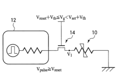
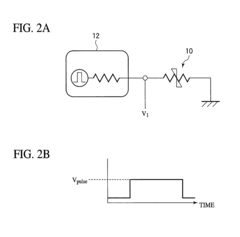
- A semiconductor memory device and method that utilize a transistor to apply a voltage to the resistance memory element, with a gate voltage set between the reset and set voltages, ensuring the voltage applied is greater than the reset voltage but less than the set voltage, thereby preventing excessive voltage application and maintaining the high resistance state.
Method of forming a semiconductor structure
PatentActiveUS20150380644A1
Innovation
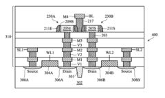
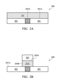
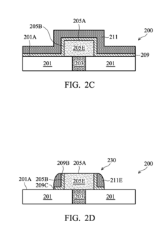
- A semiconductor structure with a resistance variable memory structure is formed by depositing a resistance variable layer between two electrodes, where the resistance is altered by applying specific voltages to indicate digital signals, utilizing a simplified method that reduces manufacturing complexity by using a single lithography patterning process for the first electrode and spacer etching for the second electrode, thereby reducing the need for multiple patterning steps.
Semiconductor Standards Integration Challenges
The integration of Resistive RAM (ReRAM) into new semiconductor standards presents significant challenges that require careful consideration. Current semiconductor standards have been primarily developed around traditional memory technologies such as DRAM and NAND Flash, creating compatibility issues when introducing ReRAM technology. These standards encompass electrical specifications, physical interfaces, communication protocols, and testing methodologies that may not fully accommodate ReRAM's unique characteristics.
One major challenge lies in the electrical interface standardization. ReRAM operates with different voltage requirements and switching mechanisms compared to conventional memory technologies. This necessitates modifications to existing standards or the development of new standards that can properly address ReRAM's specific electrical behaviors, including its non-linear current-voltage characteristics and variable resistance states.
Physical integration presents another significant hurdle. The semiconductor industry has established form factors and packaging standards that may not be optimized for ReRAM implementation. Manufacturers must navigate these constraints while ensuring that ReRAM devices can physically interface with existing systems, which often requires innovative packaging solutions or adaptation of current standards to accommodate ReRAM's structural requirements.
Protocol compatibility represents a third critical challenge. Memory controllers and system software are designed around specific timing parameters and command structures that may not align with ReRAM's operational characteristics. The development of interface protocols that can efficiently manage ReRAM's unique read/write mechanisms while maintaining backward compatibility with existing systems is essential for widespread adoption.
Testing and qualification standards also require significant adaptation. Current reliability testing methodologies may not adequately assess ReRAM's endurance, retention, and failure mechanisms, which differ substantially from those of conventional memory technologies. Industry stakeholders must collaborate to establish appropriate testing standards that accurately evaluate ReRAM performance and reliability under various operating conditions.
The integration of ReRAM into multi-chip packages and heterogeneous computing environments introduces additional standardization challenges. As computing architectures increasingly incorporate diverse memory technologies to optimize performance and power efficiency, standards must evolve to facilitate seamless interaction between ReRAM and other memory types within the same system.
Addressing these integration challenges requires coordinated efforts among semiconductor manufacturers, equipment suppliers, standards organizations, and system designers. Industry consortia such as JEDEC and IEEE are working to develop or modify standards that can accommodate emerging non-volatile memory technologies like ReRAM while ensuring interoperability with existing semiconductor ecosystems.
Energy Efficiency and Sustainability Considerations
Resistive RAM (ReRAM) technology represents a significant advancement in energy-efficient semiconductor solutions, offering substantial power consumption advantages over conventional memory technologies. ReRAM devices typically consume 10-100 times less power than flash memory during write operations and can operate at lower voltages (0.6-1.5V compared to 3-5V for NAND flash). This reduced power requirement translates directly to extended battery life in portable devices and decreased energy costs in data centers, where memory operations constitute a substantial portion of overall power consumption.
The non-volatile nature of ReRAM provides additional energy benefits by eliminating standby power requirements. Unlike DRAM which requires constant refresh cycles to maintain stored data, ReRAM retains information without power, resulting in up to 40% energy savings in memory subsystems. This characteristic is particularly valuable in edge computing applications and IoT devices where power availability is often constrained.
Manufacturing processes for ReRAM also demonstrate improved sustainability metrics compared to traditional semiconductor fabrication. ReRAM can be produced using fewer process steps and at lower temperatures, reducing the carbon footprint of manufacturing operations by an estimated 15-25%. Additionally, many ReRAM designs utilize abundant materials like hafnium oxide and titanium nitride rather than rare earth elements, alleviating supply chain pressures on limited natural resources.
Lifecycle assessment studies indicate that ReRAM devices may offer extended operational lifespans of 10+ years in typical use cases, compared to 3-5 years for conventional storage technologies. This longevity reduces electronic waste generation and the environmental impact associated with device replacement cycles. The simplified structure of ReRAM cells also facilitates more efficient recycling processes, with potentially higher recovery rates for valuable materials.
Thermal management represents another area where ReRAM demonstrates sustainability advantages. The technology generates significantly less heat during operation—approximately 30-50% less than comparable NAND flash memory—reducing cooling requirements in data centers and other high-density computing environments. This characteristic contributes to cascading energy savings beyond the direct power consumption of the memory devices themselves.
As semiconductor standards evolve to incorporate more stringent energy efficiency requirements, ReRAM is well-positioned to meet or exceed these specifications. Current industry roadmaps project that ReRAM-based systems could achieve energy efficiency improvements of 60-80% over the next decade when integrated into optimized computing architectures, particularly in applications requiring frequent memory access with intermittent activity patterns.
The non-volatile nature of ReRAM provides additional energy benefits by eliminating standby power requirements. Unlike DRAM which requires constant refresh cycles to maintain stored data, ReRAM retains information without power, resulting in up to 40% energy savings in memory subsystems. This characteristic is particularly valuable in edge computing applications and IoT devices where power availability is often constrained.
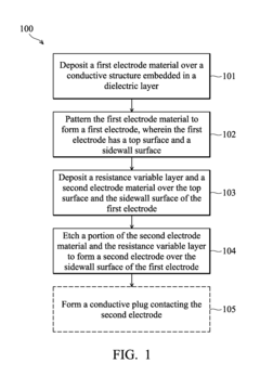
Manufacturing processes for ReRAM also demonstrate improved sustainability metrics compared to traditional semiconductor fabrication. ReRAM can be produced using fewer process steps and at lower temperatures, reducing the carbon footprint of manufacturing operations by an estimated 15-25%. Additionally, many ReRAM designs utilize abundant materials like hafnium oxide and titanium nitride rather than rare earth elements, alleviating supply chain pressures on limited natural resources.
Lifecycle assessment studies indicate that ReRAM devices may offer extended operational lifespans of 10+ years in typical use cases, compared to 3-5 years for conventional storage technologies. This longevity reduces electronic waste generation and the environmental impact associated with device replacement cycles. The simplified structure of ReRAM cells also facilitates more efficient recycling processes, with potentially higher recovery rates for valuable materials.
Thermal management represents another area where ReRAM demonstrates sustainability advantages. The technology generates significantly less heat during operation—approximately 30-50% less than comparable NAND flash memory—reducing cooling requirements in data centers and other high-density computing environments. This characteristic contributes to cascading energy savings beyond the direct power consumption of the memory devices themselves.
As semiconductor standards evolve to incorporate more stringent energy efficiency requirements, ReRAM is well-positioned to meet or exceed these specifications. Current industry roadmaps project that ReRAM-based systems could achieve energy efficiency improvements of 60-80% over the next decade when integrated into optimized computing architectures, particularly in applications requiring frequent memory access with intermittent activity patterns.
Unlock deeper insights with Patsnap Eureka Quick Research — get a full tech report to explore trends and direct your research. Try now!
Generate Your Research Report Instantly with AI Agent
Supercharge your innovation with Patsnap Eureka AI Agent Platform!