

How Resistive RAM Impacts Electronics Industry Standards
OCT 9, 20259 MIN READ
Generate Your Research Report Instantly with AI Agent
Patsnap Eureka helps you evaluate technical feasibility & market potential.
ReRAM Technology Evolution and Objectives
Resistive Random Access Memory (ReRAM) represents a significant evolution in non-volatile memory technology, emerging from decades of research into alternative memory solutions. The concept of resistance-based memory dates back to the 1960s, but meaningful development began in the early 2000s when limitations of flash memory became increasingly apparent in advanced electronic systems. ReRAM's fundamental principle leverages resistance switching phenomena in metal oxides and other materials, creating a compelling alternative to traditional memory architectures.
The technology evolution of ReRAM has been characterized by progressive improvements in material science, fabrication techniques, and circuit design. Early ReRAM prototypes suffered from reliability issues, high operating voltages, and limited endurance. However, breakthroughs in understanding the underlying physical mechanisms of filament formation and dissolution have led to substantial improvements in these parameters over the past decade.
Industry objectives for ReRAM development have centered around creating memory solutions that combine the speed of DRAM with the non-volatility of flash memory, while offering superior scalability and energy efficiency. The technology aims to address the growing "memory wall" problem in computing architectures, where memory access speeds fail to keep pace with processor advancements.
From a standards perspective, ReRAM development has been guided by the need for compatibility with existing semiconductor manufacturing processes while pushing performance boundaries. The International Technology Roadmap for Semiconductors (ITRS) has recognized ReRAM as a promising emerging memory technology, establishing performance benchmarks that have driven research and development efforts across the industry.
Current technical objectives focus on improving several key parameters: reducing switching energy requirements, enhancing endurance beyond 10^12 cycles, extending data retention beyond 10 years at elevated temperatures, and scaling devices below 10nm while maintaining performance characteristics. These objectives directly influence electronics industry standards by establishing new performance thresholds for memory subsystems.
The evolution trajectory suggests ReRAM will continue advancing toward neuromorphic computing applications, where its analog resistance states can emulate synaptic behavior. This represents a paradigm shift from binary storage to computational memory, potentially requiring entirely new standards for memory-centric computing architectures.
As ReRAM matures, industry standards bodies including JEDEC, IEEE, and SEMI are actively developing specifications to ensure interoperability, reliability testing methodologies, and integration frameworks. These standardization efforts are critical for ReRAM's broader adoption across consumer electronics, automotive systems, industrial applications, and data centers, where established standards provide the foundation for ecosystem development.
Market Demand Analysis for ReRAM Solutions
The global market for Resistive Random Access Memory (ReRAM) solutions is experiencing significant growth, driven by increasing demands for more efficient, high-performance memory technologies. Current market projections indicate that the ReRAM market is expected to grow at a compound annual growth rate of 16% between 2023 and 2030, reaching a market value of approximately 2.5 billion USD by the end of the forecast period.
The primary market demand for ReRAM stems from its potential to address critical limitations in existing memory technologies. Traditional NAND flash memory faces scaling challenges below 10nm, while DRAM struggles with power consumption and data retention issues. ReRAM offers a compelling alternative with its non-volatile characteristics, lower power consumption, and faster switching speeds.
Several key industry sectors are driving demand for ReRAM solutions. The consumer electronics segment represents the largest market share, with applications in smartphones, tablets, and wearable devices where power efficiency and performance are paramount. Market research indicates that consumer electronics manufacturers are actively seeking memory solutions that can extend battery life while maintaining or improving performance metrics.
Enterprise storage systems constitute another significant market segment, where ReRAM's potential for high-density storage and rapid data access makes it particularly attractive. Data centers are increasingly exploring ReRAM as a solution to reduce energy consumption while handling growing data volumes, with potential energy savings of up to 40% compared to conventional memory technologies.
The automotive industry represents an emerging but rapidly growing market for ReRAM, particularly with the rise of autonomous vehicles and advanced driver assistance systems (ADAS). These applications require memory solutions that can withstand extreme temperatures and offer high reliability, areas where ReRAM demonstrates significant advantages over conventional technologies.
The Internet of Things (IoT) ecosystem presents perhaps the most promising long-term growth opportunity for ReRAM. Market analysis suggests that by 2025, over 75 billion connected devices will require memory solutions that balance power efficiency, cost, and performance – precisely the attributes that ReRAM aims to deliver.
Geographically, North America and Asia-Pacific regions dominate the ReRAM market, with Asia-Pacific expected to witness the highest growth rate due to the concentration of semiconductor manufacturing facilities and consumer electronics production. China's significant investments in semiconductor technology are particularly noteworthy, as the country seeks to reduce dependence on imported memory technologies.
Customer requirements are evolving toward memory solutions that offer higher endurance cycles, improved retention times, and lower manufacturing costs. Current ReRAM solutions typically offer endurance of 10^6 to 10^9 cycles, but market demand indicates a need for further improvements to reach 10^12 cycles for enterprise applications.
ReRAM Development Status and Technical Barriers
Resistive RAM (ReRAM) technology has reached a significant development stage but continues to face several technical barriers that impede its widespread adoption. Currently, ReRAM has demonstrated promising characteristics including non-volatility, high density, low power consumption, and compatibility with CMOS processes. Leading research institutions and semiconductor companies have successfully fabricated ReRAM devices with switching speeds in the nanosecond range and endurance cycles exceeding 10^6, positioning it as a viable alternative to conventional memory technologies.
Despite these advancements, ReRAM faces substantial technical challenges. The most prominent issue is retention reliability, with many ReRAM devices struggling to maintain stored data for the industry-standard 10-year period under various temperature conditions. This reliability concern directly impacts the technology's suitability for mission-critical applications and consumer electronics where data integrity is paramount.
Variability in switching characteristics represents another significant barrier. Device-to-device and cycle-to-cycle variations in resistance states create difficulties in designing reliable sensing circuits and establishing uniform programming algorithms. This inconsistency complicates the integration of ReRAM into existing memory hierarchies and standardized interfaces.
The scaling limitations of ReRAM also present challenges. While theoretically capable of scaling below 10nm, practical implementations encounter issues with current density and thermal management at these dimensions. The sneak current problem in crossbar arrays further complicates high-density implementations, requiring additional selector devices that increase manufacturing complexity and potentially reduce the density advantage.
Material stability and compatibility issues persist across the industry. The oxide materials commonly used in ReRAM structures can degrade over time due to oxygen vacancy migration and electrode material diffusion. Finding materials that maintain stable performance while remaining compatible with standard semiconductor manufacturing processes continues to challenge researchers and manufacturers alike.
From a manufacturing perspective, ReRAM faces yield and process integration challenges. The precise control required for the formation of the switching layer and the integration of novel materials into established fabrication flows present significant hurdles. These manufacturing difficulties contribute to higher costs and slower adoption rates compared to more mature memory technologies.
Standardization efforts for ReRAM remain fragmented, with different companies pursuing proprietary approaches to overcome technical barriers. This lack of industry consensus on specifications, testing methodologies, and interface protocols hinders interoperability and slows market acceptance. Until these standardization issues are resolved, ReRAM will continue to face adoption challenges despite its promising technical characteristics.
Current ReRAM Implementation Approaches
01 Standardization of Resistive RAM Manufacturing Processes
Industry standards for manufacturing processes of Resistive RAM (RRAM) devices are essential for ensuring consistency and reliability. These standards cover various aspects including material selection, deposition techniques, and quality control measures. Standardized manufacturing processes help in achieving uniform performance characteristics across different production batches and facilities, which is crucial for mass production and commercial viability of RRAM technology.- Standardization of RRAM manufacturing processes: Industry standards for manufacturing resistive RAM (RRAM) focus on establishing consistent fabrication methods and quality control measures. These standards address critical aspects such as material selection, deposition techniques, and process parameters to ensure reliable and reproducible RRAM devices. Standardized manufacturing processes help in achieving uniform performance characteristics across different production batches and facilities, which is essential for widespread commercial adoption of RRAM technology.
- RRAM device architecture and design standards: Standards related to RRAM device architecture define specifications for cell structure, array organization, and integration with peripheral circuits. These standards establish guidelines for scaling parameters, electrode materials, switching layer compositions, and cell dimensions. Standardized design approaches help ensure compatibility between RRAM components from different manufacturers and facilitate integration with existing semiconductor technologies, enabling more efficient development of RRAM-based products.
- Testing and reliability standards for RRAM: Industry standards for testing and reliability assessment of RRAM devices establish uniform methodologies for evaluating performance metrics such as endurance, retention, and switching characteristics. These standards define test conditions, measurement protocols, and acceptance criteria to ensure consistent evaluation across the industry. Standardized reliability testing helps identify failure mechanisms and enables meaningful comparison between different RRAM technologies, supporting quality assurance in commercial applications.
- RRAM interface and communication protocols: Standards for RRAM interfaces and communication protocols define how RRAM devices interact with host systems and other memory components. These standards establish signal timing, command structures, addressing schemes, and data transfer protocols specific to RRAM characteristics. Standardized interfaces ensure interoperability between RRAM modules and memory controllers from different manufacturers, facilitating the integration of RRAM into existing computing architectures and memory hierarchies.
- RRAM application-specific standards: Application-specific standards for RRAM address requirements for particular use cases such as neuromorphic computing, IoT devices, and embedded systems. These standards define performance parameters, power consumption limits, and form factors tailored to specific application domains. By establishing specialized standards for different market segments, the industry ensures that RRAM technology can be effectively optimized for diverse applications while maintaining necessary compatibility and reliability benchmarks.
02 Testing and Reliability Standards for RRAM Devices
Testing and reliability standards for Resistive RAM devices establish protocols for evaluating performance metrics such as endurance, retention time, and switching speed. These standards define test conditions, measurement methodologies, and acceptance criteria to ensure that RRAM devices meet industry requirements. Standardized testing procedures enable fair comparison between different RRAM technologies and help in identifying potential failure mechanisms, ultimately improving the overall reliability of RRAM-based products.Expand Specific Solutions03 Interface and Compatibility Standards for RRAM Integration
Interface and compatibility standards for Resistive RAM focus on ensuring seamless integration with existing semiconductor technologies and systems. These standards define electrical specifications, signal protocols, and physical interfaces required for RRAM devices to work with conventional memory controllers and systems. Standardized interfaces facilitate the adoption of RRAM technology by enabling compatibility with existing hardware and software ecosystems, reducing implementation barriers for system designers.Expand Specific Solutions04 Data Storage and Security Standards for RRAM Applications
Data storage and security standards for Resistive RAM applications establish protocols for data integrity, encryption, and protection against unauthorized access. These standards define requirements for secure data storage, retrieval operations, and protection mechanisms against potential vulnerabilities. Standardized security features are particularly important for RRAM applications in sensitive areas such as financial transactions, personal data storage, and military systems where data protection is paramount.Expand Specific Solutions05 Power Consumption and Performance Benchmarking Standards
Power consumption and performance benchmarking standards for Resistive RAM technology establish metrics and methodologies for evaluating energy efficiency and operational characteristics. These standards define parameters such as read/write energy, standby power, and performance under various operating conditions. Standardized benchmarking enables objective comparison between different RRAM technologies and helps in identifying optimal solutions for specific applications, particularly in power-sensitive environments such as mobile devices and IoT applications.Expand Specific Solutions
Key Industry Players in ReRAM Development
Resistive RAM (ReRAM) technology is currently in a transitional phase from research to early commercialization, with the global market projected to reach $4-5 billion by 2025. The competitive landscape features established semiconductor giants like Samsung, TSMC, and Intel investing heavily in ReRAM development alongside specialized players such as Winbond, KIOXIA, and Macronix. Technical maturity varies significantly, with most companies at the advanced prototype or early production stage. Industry leaders like IBM and Samsung have demonstrated working ReRAM cells with impressive performance metrics, while companies like Adesto and Nantero have introduced initial commercial products. Academic-industry partnerships involving institutions like Peking University and the Industrial Technology Research Institute are accelerating standardization efforts, though widespread adoption faces challenges in scaling, endurance, and integration with existing manufacturing processes.
Samsung Electronics Co., Ltd.
Technical Solution: Samsung has developed advanced Resistive RAM (ReRAM) technology as part of their memory portfolio. Their approach integrates ReRAM cells with conventional CMOS technology, creating high-density, low-power memory solutions. Samsung's ReRAM architecture employs a metal-oxide-metal structure with a transition metal oxide layer that changes resistance states when voltage is applied. Their implementation focuses on multi-level cell capabilities, allowing storage of multiple bits per cell to increase memory density. Samsung has demonstrated ReRAM devices with sub-10nm feature sizes and switching speeds in nanoseconds, positioning them for both storage and computing applications[1]. They've also pioneered 3D vertical integration of ReRAM cells to maximize storage density while minimizing footprint, crucial for mobile and IoT applications where space constraints are significant[3].
Strengths: Samsung's extensive manufacturing infrastructure enables rapid scaling and commercialization of ReRAM technology. Their vertical integration allows optimization across device design, fabrication, and system integration. Weaknesses: As an established memory manufacturer, Samsung must balance investment in emerging ReRAM technology against their substantial commitments to established DRAM and NAND flash production lines.
KIOXIA Corp.
Technical Solution: KIOXIA (formerly Toshiba Memory) has developed advanced ReRAM technology as part of their storage class memory portfolio. Their approach uses metal oxide-based resistive elements arranged in crossbar arrays to create high-density, non-volatile memory solutions. KIOXIA's ReRAM implementation features multi-layer stacking capabilities, allowing vertical integration of memory cells to maximize storage density. Their technology demonstrates excellent scalability, with demonstrated devices at sub-20nm feature sizes and clear pathways to further miniaturization[9]. KIOXIA has focused on optimizing ReRAM for storage class memory applications that bridge the performance gap between DRAM and NAND flash. Their architecture supports byte-addressability with access times in tens of nanoseconds, significantly faster than conventional flash memory. KIOXIA has also developed specialized controller technologies to manage ReRAM-specific characteristics like resistance drift and variability, ensuring long-term data retention and reliability. Their research has demonstrated ReRAM arrays with endurance exceeding 10^6 cycles and data retention periods of over 10 years at operating temperatures[10].
Strengths: KIOXIA's extensive experience in memory manufacturing provides established production capabilities and channels to market. Their position as a leading NAND supplier gives them insight into storage system requirements and customer needs. Weaknesses: As a major flash memory producer, KIOXIA must carefully manage the potential cannibalization of their existing product lines as they introduce disruptive ReRAM technology.
Critical ReRAM Patents and Technical Innovations
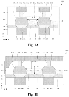
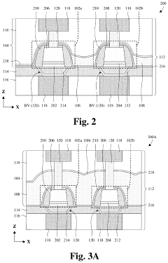
Resistive random-access memory cells
PatentActiveUS20160196874A1
Innovation
- The introduction of an electrically-conductive component within the RRAM cell structure, which allows for programmable cell states by varying the resistance of the conductive path and insulating matrix, enabling effective differentiation of high-resistance states and reducing sneak-path currents without destructive read operations.
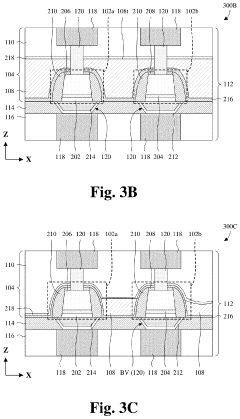
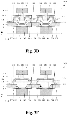
Memory cells separated by a void-free dielectric structure
PatentActiveUS11839090B2
Innovation
- A method involving the deposition of an inter-cell filler layer using a high aspect ratio (HAR) deposition process, followed by recessing to ensure a void-free dielectric structure, which reduces the aspect ratio and prevents void formation in the inter-cell areas, thereby enhancing the reliability of the RRAM array by reducing dielectric breakdown risk.
Industry Standards Adaptation for ReRAM Integration
The integration of Resistive RAM (ReRAM) into mainstream electronics necessitates significant adaptations to existing industry standards. Currently, memory interface standards like JEDEC's DDR, LPDDR, and HBM are optimized for traditional volatile memory technologies with different electrical characteristics and timing requirements than ReRAM. These standards require comprehensive revisions to accommodate ReRAM's unique attributes such as non-volatility, different read/write mechanisms, and endurance parameters.
Storage interface standards including NVMe, UFS, and eMMC also need modification to leverage ReRAM's capabilities effectively. The development of hybrid standards that can address both memory and storage functionalities becomes crucial as ReRAM blurs the traditional boundary between these two domains. This convergence represents a fundamental shift in how data storage hierarchies are standardized.
Reliability and testing standards present another critical area requiring adaptation. JEDEC's JESD47 and JESD22 standards for semiconductor device qualification must incorporate new test methodologies specific to ReRAM's failure modes, retention characteristics, and endurance profiles. The industry needs standardized approaches to measure and guarantee ReRAM performance across varied environmental conditions and use cases.
Power management standards face revision requirements as well. While ReRAM offers inherent advantages in power consumption compared to DRAM, existing power management protocols in standards like ACPI and various low-power specifications need updates to optimize system-level energy efficiency when incorporating ReRAM components. These modifications would enable electronics to fully capitalize on ReRAM's non-volatile nature for power saving.
Form factor and packaging standards represent another dimension requiring adaptation. Current physical specifications for memory modules, cards, and embedded solutions must evolve to accommodate ReRAM's integration into system architectures. This may include new pin configurations, signal requirements, or thermal considerations specific to ReRAM technology.
Security standards also need enhancement to leverage ReRAM's potential for hardware-based security features. Standards bodies like ISO, IEC, and NIST must develop or modify existing security frameworks to incorporate ReRAM's capabilities for secure storage, physical unclonable functions, and tamper resistance.
The timeline for these standards adaptations varies across different application domains. Consumer electronics standards may evolve more rapidly, while mission-critical sectors like automotive, aerospace, and medical devices require more extensive validation periods before standard revisions can be implemented. This creates a complex standardization landscape that industry stakeholders must navigate as ReRAM adoption accelerates.
Environmental Impact and Sustainability of ReRAM Technology
The environmental impact of Resistive RAM (ReRAM) technology represents a significant advancement in sustainable electronics manufacturing compared to conventional memory technologies. ReRAM devices require fewer raw materials during production, with manufacturing processes that consume approximately 30-40% less energy than traditional DRAM or flash memory fabrication. This reduction stems from simpler structure designs and fewer processing steps, directly translating to lower carbon emissions throughout the production lifecycle.
ReRAM's operational efficiency further enhances its sustainability profile. The technology's non-volatile nature eliminates standby power consumption, while its lower operating voltages (typically 0.5-2V compared to 3-5V for conventional memories) result in substantial energy savings during device operation. Studies indicate that ReRAM-based systems can achieve up to 60% reduction in power consumption for memory operations, contributing significantly to reduced carbon footprints in data centers and consumer electronics.
End-of-life considerations also favor ReRAM technology. The devices contain fewer toxic materials compared to conventional memory technologies, with most ReRAM structures utilizing simple metal oxides rather than heavy metals or complex compounds. This composition simplifies recycling processes and reduces environmental contamination risks when devices are discarded.
The manufacturing scalability of ReRAM offers additional environmental benefits. The technology's compatibility with existing CMOS fabrication infrastructure means minimal investment in new manufacturing equipment is required for production scaling. This reuse of existing infrastructure prevents the environmental impact associated with developing and deploying entirely new manufacturing systems.
Resource conservation represents another critical sustainability advantage. ReRAM's higher density capabilities mean more storage capacity per unit of physical materials, potentially reducing the overall material footprint of electronic devices. Additionally, the extended write endurance (10^6-10^12 cycles versus 10^4-10^5 for flash) extends device lifespans, reducing electronic waste generation rates.
Looking forward, ReRAM's potential to enable more energy-efficient computing architectures, particularly in-memory computing and neuromorphic systems, promises further environmental benefits. These architectures could reduce data movement between processing and memory units, addressing one of computing's most energy-intensive operations and potentially reducing overall system energy requirements by 70-80% for specific workloads.
Unlock deeper insights with Patsnap Eureka Quick Research — get a full tech report to explore trends and direct your research. Try now!
Generate Your Research Report Instantly with AI Agent
Supercharge your innovation with Patsnap Eureka AI Agent Platform!