Material Trends in Resistive RAM: A Market Analysis
OCT 9, 20259 MIN READ
Generate Your Research Report Instantly with AI Agent
Patsnap Eureka helps you evaluate technical feasibility & market potential.
ReRAM Technology Evolution and Objectives
Resistive Random Access Memory (ReRAM) has evolved significantly since its conceptual introduction in the 1960s. The technology gained substantial research momentum in the early 2000s when limitations of conventional memory technologies became increasingly apparent. ReRAM's development trajectory has been driven by the semiconductor industry's pursuit of non-volatile memory solutions that combine the speed of SRAM and DRAM with the persistence of flash memory, while overcoming scaling limitations of traditional technologies.
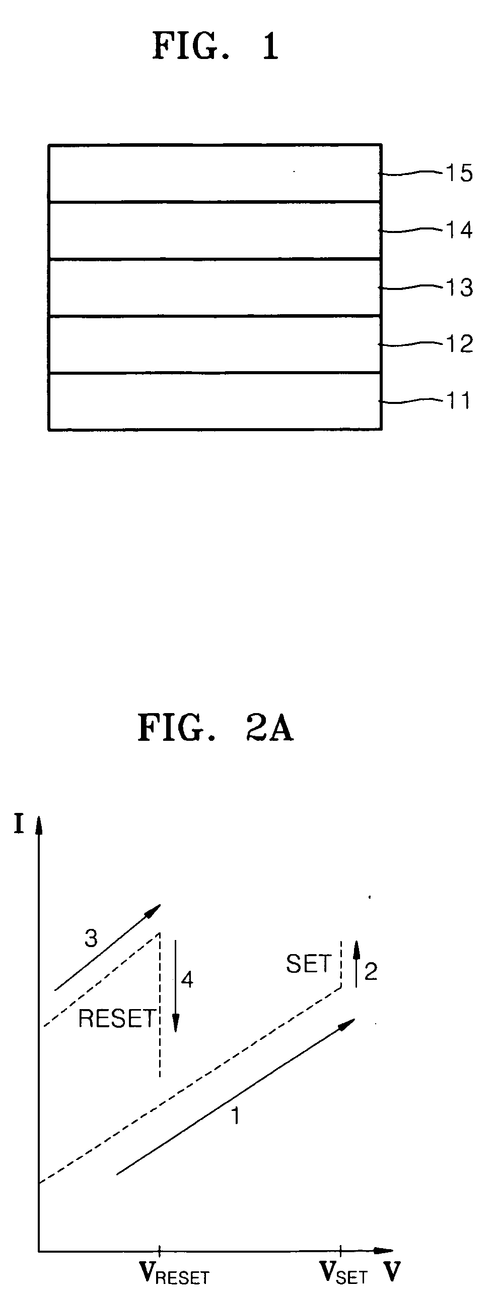
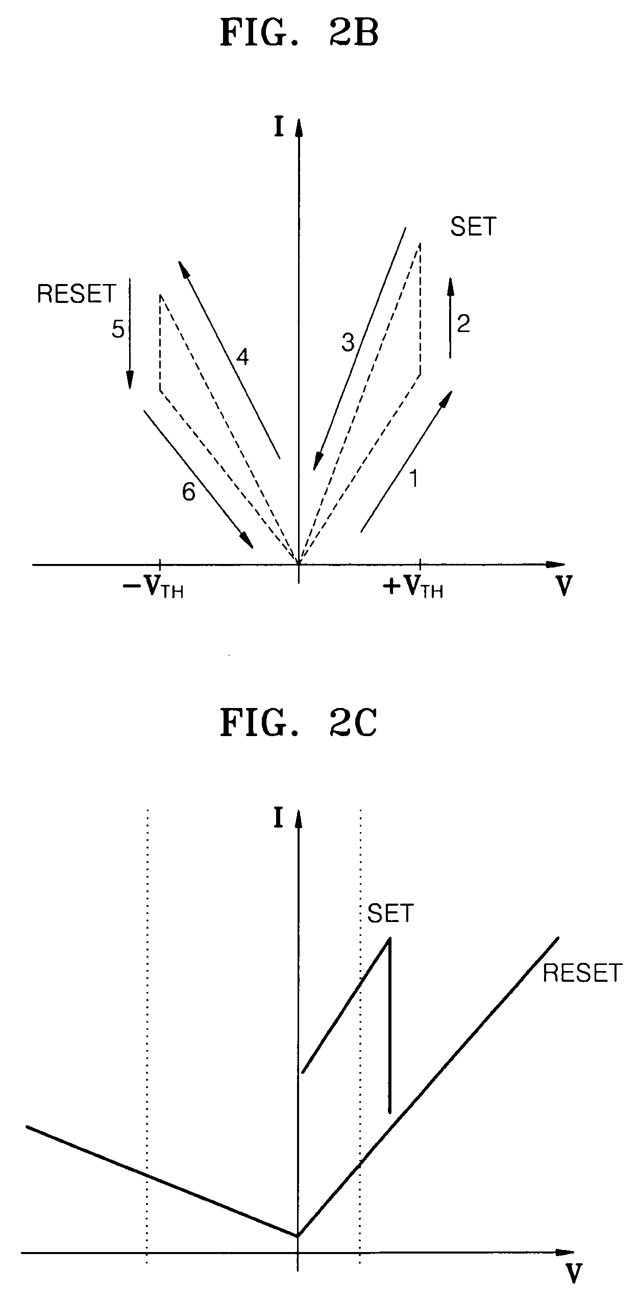
The fundamental operating principle of ReRAM relies on resistance switching phenomena in metal-oxide materials, where electrical resistance can be altered between high and low states through the formation and disruption of conductive filaments. This mechanism enables data storage without constant power supply, offering significant advantages for energy-efficient computing applications.
Industry evolution has progressed through several distinct phases: initial proof-of-concept demonstrations (2000-2005), material optimization and scaling studies (2006-2012), manufacturing process development (2013-2018), and current commercialization efforts focusing on specialized applications (2019-present). Each phase has contributed to addressing critical challenges in reliability, endurance, and integration with CMOS processes.
The primary technological objectives for ReRAM development include achieving higher density storage capabilities while maintaining low power consumption. Current targets aim for sub-10nm feature sizes, endurance exceeding 10^12 cycles, and retention times of over 10 years at operating temperatures up to 85°C. These parameters are essential for ReRAM to compete effectively with established memory technologies in various application domains.
Material innovation represents the cornerstone of ReRAM advancement, with research focusing on binary metal oxides (HfOx, TaOx), perovskite structures, and complex chalcogenide compounds. Each material system offers distinct advantages in terms of switching speed, power consumption, and compatibility with existing fabrication processes. The trend toward multi-layer stacking and 3D architectures further enhances storage density potential.
Looking forward, ReRAM technology aims to position itself as a universal memory solution, potentially bridging the performance gap between storage and computing elements in next-generation computing architectures. This includes neuromorphic computing applications, where ReRAM's analog resistance states can emulate synaptic behavior for artificial neural networks, and in-memory computing paradigms that reduce data movement between processing and storage units.
The convergence of material science advancements with novel device architectures represents the most promising direction for achieving these ambitious technological objectives, potentially revolutionizing memory hierarchy in computing systems within the next decade.
Market Demand Analysis for ReRAM Solutions
The global market for Resistive Random Access Memory (ReRAM) solutions is experiencing significant growth, driven by increasing demand for high-performance, energy-efficient memory technologies. Current market projections indicate that the ReRAM market is expected to grow at a compound annual growth rate of 16% between 2023 and 2030, reaching a market value of approximately 1.2 billion USD by 2030. This growth trajectory reflects the expanding applications of ReRAM across multiple sectors.
The primary market demand for ReRAM stems from the Internet of Things (IoT) sector, where low power consumption and non-volatility are critical requirements. As IoT device deployments continue to accelerate globally, the need for memory solutions that can operate efficiently with minimal energy consumption has become paramount. ReRAM's ability to retain data without power makes it particularly suitable for edge computing applications where devices operate on limited battery power.
Consumer electronics represents another significant market segment driving ReRAM demand. Smartphone manufacturers are increasingly exploring ReRAM technology to enhance device performance while reducing power consumption. The rapid read/write capabilities and high endurance of ReRAM make it an attractive alternative to existing flash memory solutions in mobile devices.
In the automotive sector, the transition toward autonomous vehicles and advanced driver assistance systems (ADAS) has created substantial demand for reliable, high-performance memory solutions. ReRAM's radiation hardness and temperature stability make it well-suited for automotive applications where operating conditions can be challenging. Industry analysts predict that automotive applications will account for approximately 18% of the total ReRAM market by 2028.
Enterprise storage systems represent another growing market for ReRAM solutions. Data centers are increasingly adopting ReRAM for cache memory applications due to its combination of speed and non-volatility. The technology's potential to bridge the performance gap between DRAM and NAND flash is particularly valuable in storage hierarchies where both speed and persistence are required.
Market research indicates regional variations in ReRAM adoption. Asia-Pacific currently leads in market share, with significant investments from major semiconductor manufacturers in South Korea, Japan, and Taiwan. North America follows closely, driven primarily by data center applications and military/aerospace requirements.
Customer surveys reveal that key purchasing factors for ReRAM solutions include cost per bit, endurance cycles, and integration compatibility with existing semiconductor processes. While current ReRAM solutions command a premium price compared to conventional memory technologies, the total cost of ownership advantages—including reduced power consumption and improved system performance—are increasingly recognized by end-users.
Current Material Challenges in ReRAM Development
Despite significant advancements in ReRAM technology, several material-related challenges continue to impede its widespread commercial adoption. The primary challenge remains the selection of optimal switching materials that can simultaneously deliver high endurance, long retention, fast switching speed, and low power consumption. Current metal oxide materials such as HfOx, TaOx, and TiOx exhibit trade-offs between these critical parameters, making it difficult to satisfy all requirements concurrently.
Variability in switching behavior represents another significant hurdle. Device-to-device and cycle-to-cycle variations stem from the stochastic nature of filament formation and rupture processes. This inconsistency manifests as fluctuations in SET/RESET voltages and resistance states, complicating reliable multi-level cell operation essential for high-density storage applications.
Interface engineering between the switching layer and electrodes presents complex challenges. The electrode material significantly influences the formation of conductive filaments, with noble metals like Pt showing different behaviors compared to reactive metals like Ti. Controlling these interfaces at the atomic level remains difficult but crucial for device performance optimization.
Scaling issues become increasingly prominent as ReRAM devices approach sub-10nm dimensions. At these scales, material defects and interface effects become disproportionately influential, potentially compromising device reliability. Additionally, as cell size decreases, the statistical variation in filament formation increases, further exacerbating consistency problems.
The integration of novel materials into existing CMOS fabrication processes presents compatibility challenges. Many promising ReRAM materials require processing conditions that may damage surrounding CMOS components or introduce contamination. Finding materials that can withstand back-end-of-line thermal budgets while maintaining desired switching characteristics remains problematic.
Retention and endurance degradation mechanisms are not fully understood at the material science level. Environmental factors such as temperature and humidity can accelerate degradation through ion migration or oxidation processes. Current materials struggle to maintain performance across the wide temperature ranges required for automotive and industrial applications.
Emerging applications demand specialized material properties beyond traditional memory requirements. Neuromorphic computing applications require materials exhibiting analog resistance modulation with high precision, while security applications need materials with unique physical unclonable properties. The development of materials optimized for these specific use cases rather than general memory applications represents a significant shift in research focus.
Current Material Solutions for ReRAM Devices
01 Metal oxide-based resistive RAM materials
Metal oxides are widely used as resistive switching materials in ReRAM devices due to their excellent electrical properties and compatibility with semiconductor manufacturing processes. These materials include transition metal oxides such as hafnium oxide, titanium oxide, and tantalum oxide, which exhibit reliable resistive switching behavior through the formation and rupture of conductive filaments. The oxygen vacancy movement within these metal oxides enables the reversible switching between high and low resistance states, making them suitable for non-volatile memory applications.- Metal oxide-based resistive RAM materials: Metal oxides are widely used as switching materials in resistive RAM devices due to their excellent switching characteristics and compatibility with CMOS technology. These materials form conductive filaments through oxygen vacancy migration under an electric field, enabling reversible resistance switching. Common metal oxides include hafnium oxide, titanium oxide, tantalum oxide, and nickel oxide, which offer different performance characteristics in terms of switching speed, endurance, and retention time.
- Chalcogenide-based resistive RAM materials: Chalcogenide materials, particularly those containing elements like sulfur, selenium, and tellurium, are important for phase-change memory applications in resistive RAM. These materials can switch between amorphous and crystalline states with different resistance levels when subjected to electrical pulses. The phase change mechanism provides stable and reliable memory storage with good data retention properties and multi-level cell capabilities, making them suitable for high-density storage applications.
- Polymer and organic resistive RAM materials: Polymer and organic materials offer unique advantages for resistive RAM applications, including flexibility, low-cost processing, and compatibility with large-area electronics. These materials typically operate through conformational changes or charge trapping mechanisms when subjected to electrical stimuli. Organic resistive RAM can be fabricated using solution processing techniques at low temperatures, making them suitable for flexible electronics and printed memory applications.
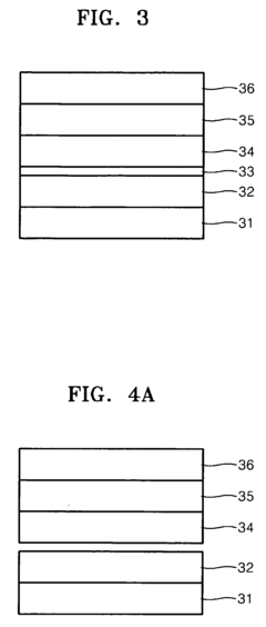
- Composite and multilayer resistive RAM structures: Composite and multilayer structures combine different materials to enhance the performance of resistive RAM devices. These structures often include barrier layers, electrode materials, and multiple switching layers to optimize switching characteristics, reduce operating voltages, and improve reliability. The interfaces between different materials play a crucial role in the switching mechanism, allowing for engineered performance through careful material selection and deposition techniques.
- Doped and engineered resistive RAM materials: Doping and material engineering approaches are used to enhance the performance of resistive RAM materials. By introducing specific dopants or controlling defect concentrations, researchers can tune the switching characteristics, reduce variability, and improve endurance. Common dopants include nitrogen, silicon, and various metals that modify the electronic properties and oxygen vacancy dynamics in oxide-based materials. Engineered materials with controlled stoichiometry and defect profiles show improved switching uniformity and reliability.
02 Chalcogenide-based resistive RAM materials
Chalcogenide materials, particularly those containing elements such as sulfur, selenium, and tellurium, are employed in resistive RAM devices for their phase-change properties. These materials can switch between amorphous and crystalline states with different resistivity levels when subjected to electrical pulses. The ability to rapidly and reversibly transition between these states makes chalcogenide-based materials attractive for high-speed memory applications. Their excellent scalability and multi-level cell capability further enhance their potential for next-generation non-volatile memory technologies.Expand Specific Solutions03 Polymer and organic resistive RAM materials
Polymer and organic materials offer unique advantages for resistive RAM applications, including flexibility, low-cost processing, and biocompatibility. These materials exhibit resistive switching through mechanisms such as charge trapping, conformational changes, or redox reactions. Conductive polymers and organic compounds can be engineered to achieve stable and reproducible switching characteristics. The ability to fabricate these devices using solution processing techniques at low temperatures makes them particularly suitable for flexible electronics and biodegradable memory applications.Expand Specific Solutions04 Perovskite and complex oxide resistive RAM materials
Perovskite and complex oxide materials with the general formula ABO₃ demonstrate excellent resistive switching properties for ReRAM applications. These materials, including strontium titanate, barium titanate, and various manganites, exhibit unique electronic properties due to their crystal structure and composition. The resistive switching in these materials often involves oxygen vacancy migration and interface effects. Their tunable electrical properties through doping and composition modification allow for customized memory performance characteristics, including multi-level storage capabilities and improved retention times.Expand Specific Solutions05 Fabrication techniques and device structures for resistive RAM
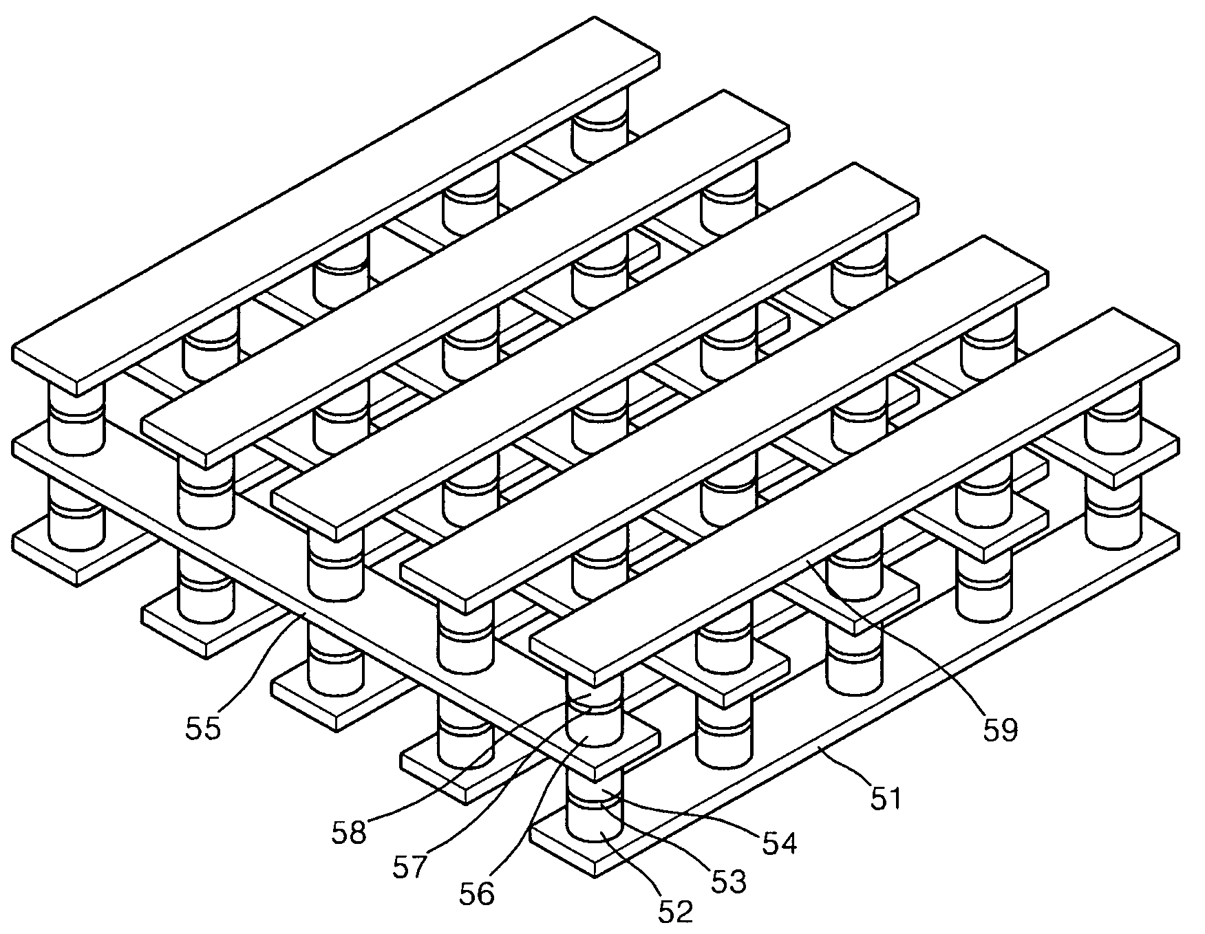
Advanced fabrication techniques and innovative device structures are crucial for optimizing resistive RAM performance. These include atomic layer deposition for precise thickness control, interface engineering to enhance switching characteristics, and the integration of selector devices to mitigate sneak path issues in crossbar arrays. Three-dimensional stacking architectures enable high-density memory integration, while novel electrode materials improve device reliability and endurance. The development of these fabrication methods and structures addresses key challenges in resistive RAM technology, such as variability, endurance, and power consumption.Expand Specific Solutions
Key Industry Players in ReRAM Manufacturing
The Resistive RAM (ReRAM) market is currently in a growth phase, transitioning from early adoption to mainstream implementation, with market size projected to reach significant expansion due to increasing demand for non-volatile memory solutions. The technology maturity varies across key players, with Samsung Electronics, Micron Technology, and SK hynix leading in commercial deployment of ReRAM technologies. Companies like KIOXIA, Winbond, and Macronix are advancing rapidly with innovative material solutions, while research institutions such as ITRI and universities (Peking, Fudan) are driving fundamental material innovations. TSMC and UMC provide critical manufacturing infrastructure, while emerging players like Adesto Technologies offer specialized ReRAM solutions for IoT applications. The competitive landscape shows established semiconductor giants competing with specialized memory manufacturers and research-backed startups in developing next-generation ReRAM materials.
Samsung Electronics Co., Ltd.
Technical Solution: Samsung has pioneered advanced RRAM technologies with their proprietary cell structure design that utilizes metal oxide materials (primarily HfO2 and TaOx) for filament formation. Their approach incorporates a unique bilayer switching layer that enhances retention while maintaining low operating voltages (typically <3V). Samsung's RRAM implementation features a crossbar array architecture that achieves high density (>10Gb/cm²) while addressing sneak path issues through selector devices integrated with memory cells. Their technology demonstrates excellent endurance (>10⁶ cycles) and fast switching speeds (<50ns), positioning it for both storage class memory and neuromorphic computing applications. Samsung has successfully demonstrated 3D stacked RRAM arrays with up to 8 layers, significantly increasing storage density while maintaining performance metrics. Recent developments include integration with their advanced logic processes (5nm and below) for embedded applications requiring ultra-low power consumption[1][3].
Strengths: Industry-leading manufacturing capabilities allow for rapid scaling and commercialization; extensive IP portfolio in materials science; strong system-level integration expertise with their own SoC designs. Weaknesses: Higher production costs compared to some competitors; technology still faces challenges in long-term data retention at smaller nodes; requires complex selector devices to maintain performance in high-density arrays.
KIOXIA Corp.
Technical Solution: KIOXIA (formerly Toshiba Memory) has developed an innovative RRAM technology based on their proprietary metal oxide material system. Their approach utilizes a tantalum oxide (TaOx) switching layer with carefully engineered oxygen vacancy distribution to control filament formation and dissolution. KIOXIA's RRAM cells feature asymmetric electrodes (typically Pt and TiN) that create an internal electric field enhancing switching reliability. Their technology demonstrates multi-level cell (MLC) capability, storing 2-3 bits per cell through precise resistance state control, significantly increasing storage density. KIOXIA has integrated their RRAM technology with advanced 3D stacking techniques, achieving vertical integration similar to their BiCS flash architecture. Their RRAM shows impressive performance metrics including sub-10ns switching speeds, endurance exceeding 10⁷ cycles, and retention times projected to exceed 10 years at 85°C. Recent developments include embedding RRAM arrays within logic chips for edge AI applications, leveraging the technology's low power consumption (approximately 10pJ per switching operation) and analog computing capabilities[4][7].
Strengths: Strong expertise in non-volatile memory manufacturing; established relationships with major electronics manufacturers; advanced materials engineering capabilities. Weaknesses: Relatively new brand identity following separation from Toshiba; faces intense competition from larger memory manufacturers; technology still requires optimization for cost-effective mass production.
Critical Material Patents and Research Breakthroughs
Resistive random access memory with high uniformity and low power consumption and method for fabricating the same
PatentInactiveUS20160225987A1
Innovation
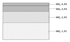
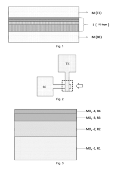
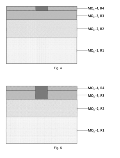
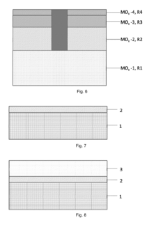
- A four-layer resistive material film structure with increasing oxygen concentrations and decreasing thicknesses is used, allowing for controlled formation and rupture of conductive filaments, enabling 2-bit storage with high uniformity and low power consumption, and potentially achieving 3-bit or higher density storage by adjusting resistance values in each layer.
Resistive random access memory
PatentInactiveUS20090302315A1
Innovation
- A RRAM design that eliminates the need for a diode or transistor structure, using a switch region with bi-polar properties and a memory resistor with uni-polar properties, formed from materials like SiO2, Ni oxides, and a nano bridge with an electrolyte intermediate layer, allowing for variable resistance and efficient data storage.
Supply Chain Analysis for ReRAM Materials
The ReRAM supply chain represents a complex ecosystem involving multiple stakeholders across various geographical regions. Material suppliers form the foundation of this chain, providing essential components such as transition metal oxides (TMOs), electrode materials, and dopants. Key suppliers include Shin-Etsu Chemical, BASF, and Dow Chemical, who have established significant market presence through their high-purity material offerings specifically tailored for ReRAM applications.
Manufacturing equipment vendors constitute another critical segment, with companies like Applied Materials, Tokyo Electron, and Lam Research developing specialized deposition and etching tools optimized for ReRAM fabrication processes. These tools enable precise control over film thickness and composition, which directly impacts device performance and reliability. The equipment market has seen substantial growth as ReRAM moves from research to production environments.
Foundry services represent a pivotal link in the ReRAM supply chain. Major players including TSMC, GlobalFoundries, and UMC have developed dedicated process modules for ReRAM integration. These foundries offer various integration options, from standalone ReRAM chips to embedded solutions within CMOS platforms, providing flexibility for different application requirements.
Material qualification and testing services have emerged as a specialized sector within the supply chain. Companies like Intertek and SGS provide comprehensive material characterization and reliability testing specifically for ReRAM materials, ensuring consistency and performance across production batches. This segment has become increasingly important as ReRAM approaches mass production phases.
Regional distribution of the supply chain shows interesting patterns, with material suppliers concentrated in Japan, South Korea, and Germany, while equipment vendors are primarily based in the United States and Japan. Foundry services are dominated by Taiwan and Singapore, creating a globally distributed value chain that presents both opportunities and challenges for supply chain management.
Vertical integration trends are becoming more pronounced, with several major memory manufacturers acquiring material suppliers to secure proprietary formulations and ensure supply stability. This consolidation reflects the strategic importance of material innovation in the ReRAM competitive landscape and highlights the value placed on intellectual property related to material compositions.
Supply chain vulnerabilities exist primarily around certain rare earth elements and specialized deposition equipment, creating potential bottlenecks that could impact scaling capabilities. Industry consortia have formed to address these challenges through standardization efforts and alternative material research programs.
Environmental Impact of ReRAM Materials
The environmental impact of ReRAM materials represents a critical consideration in the sustainable development of next-generation memory technologies. ReRAM devices utilize various metal oxides and electrode materials that require careful assessment regarding their ecological footprint throughout the entire product lifecycle.
Primary ReRAM materials such as hafnium oxide, titanium oxide, and tantalum oxide present different environmental challenges. Hafnium, while offering excellent performance characteristics, is relatively rare and energy-intensive to extract and refine. The mining processes associated with these materials can lead to habitat disruption, water pollution, and significant carbon emissions, particularly in regions with less stringent environmental regulations.
Manufacturing processes for ReRAM involve multiple deposition techniques including atomic layer deposition (ALD) and physical vapor deposition (PVD), which consume substantial energy and utilize potentially harmful precursor chemicals. However, compared to conventional flash memory fabrication, ReRAM manufacturing generally requires fewer process steps and potentially lower temperatures, resulting in reduced energy consumption per device.
The operational phase of ReRAM demonstrates promising environmental advantages. The non-volatile nature and low power requirements of ReRAM translate to significant energy savings during device operation. Studies indicate that ReRAM-based systems can achieve up to 60% reduction in energy consumption compared to conventional memory technologies, contributing to lower carbon emissions throughout the product lifespan.
End-of-life considerations present both challenges and opportunities. The complex material composition of ReRAM devices complicates recycling efforts, as separating the thin-film metal oxides from substrates requires specialized processes. However, the relatively small quantities of precious metals used in ReRAM compared to some other technologies may reduce the overall material footprint.
Recent industry initiatives have focused on developing more environmentally friendly ReRAM materials. Research into silicon-based ReRAM offers potential reductions in toxic material usage, while carbon-based ReRAM utilizing graphene and other carbon allotropes presents biodegradable alternatives that could significantly reduce end-of-life environmental impact.
Regulatory frameworks worldwide are increasingly addressing electronic waste management and restricting hazardous substances, driving manufacturers toward more sustainable material choices. Companies developing ReRAM technologies must navigate these evolving regulations while maintaining competitive performance characteristics, creating both challenges and innovation opportunities in material selection and processing techniques.
Unlock deeper insights with Patsnap Eureka Quick Research — get a full tech report to explore trends and direct your research. Try now!
Generate Your Research Report Instantly with AI Agent
Supercharge your innovation with Patsnap Eureka AI Agent Platform!