

The Interface Between Resistive RAM and Electronics Protocols
OCT 9, 20259 MIN READ
Generate Your Research Report Instantly with AI Agent
PatSnap Eureka helps you evaluate technical feasibility & market potential.
ReRAM Technology Background and Objectives
Resistive Random Access Memory (ReRAM) has emerged as a promising non-volatile memory technology over the past two decades, evolving from theoretical concepts in the 1960s to practical implementations in the 2010s. This technology leverages the resistance switching phenomenon in certain metal oxides and other materials to store binary information, offering significant advantages over conventional memory technologies including lower power consumption, higher density, and faster switching speeds.
The evolution of ReRAM technology has been marked by several key milestones, beginning with the discovery of resistance switching in metal oxides, followed by the development of reliable switching mechanisms, and culminating in the integration of ReRAM cells into commercial memory arrays. Recent advancements have focused on improving endurance, retention, and reliability while reducing power consumption and cell size.
Current technological trends in ReRAM development include the exploration of novel materials such as hafnium oxide, tantalum oxide, and various perovskites, which offer improved performance characteristics. Additionally, there is growing interest in three-dimensional architectures and multi-level cell configurations to increase storage density and efficiency.
The interface between ReRAM and electronic protocols represents a critical junction in the memory ecosystem, determining how this emerging technology can be effectively integrated into existing computing frameworks. Traditional memory interfaces were designed for technologies with fundamentally different operational characteristics, creating significant challenges for ReRAM implementation.
The primary technical objectives for ReRAM interface development include establishing standardized communication protocols that accommodate ReRAM's unique operational parameters, optimizing signal integrity for reliable data transfer, and developing efficient addressing schemes that leverage ReRAM's crossbar architecture. Additionally, there is a need to create power management protocols that capitalize on ReRAM's low energy requirements while ensuring data integrity during power transitions.
Another crucial objective is to develop interface technologies that enable seamless integration of ReRAM into heterogeneous memory systems, allowing it to coexist with and complement other memory technologies such as DRAM, NAND flash, and emerging alternatives. This requires sophisticated memory controllers capable of managing different access patterns, latency requirements, and endurance characteristics.
Looking forward, the interface technology must also anticipate future developments in ReRAM, including neuromorphic computing applications, in-memory processing capabilities, and quantum-resistant security features. These forward-looking considerations will ensure that the interface architecture remains relevant as ReRAM technology continues to evolve and expand into new application domains.
Market Demand Analysis for ReRAM Solutions
The global market for Resistive Random Access Memory (ReRAM) solutions is experiencing significant growth, driven by increasing demands for more efficient, high-performance, and low-power memory technologies. Current projections indicate that the ReRAM market is expected to reach $1.6 billion by 2025, with a compound annual growth rate of approximately 40% from 2020 to 2025.
The primary market demand for ReRAM stems from its potential to bridge the performance gap between DRAM and NAND flash memory, offering a compelling alternative in the memory hierarchy. This demand is particularly pronounced in data-intensive applications where traditional memory technologies face limitations in terms of speed, power consumption, and endurance.
In the consumer electronics sector, ReRAM is gaining traction due to its non-volatile nature, fast read/write speeds, and low power consumption. Smartphone manufacturers are exploring ReRAM integration to enhance device performance while extending battery life. The wearable technology market also presents significant opportunities, with ReRAM's small form factor and energy efficiency making it ideal for space-constrained devices.
Enterprise storage systems represent another substantial market segment for ReRAM solutions. As organizations grapple with exponential data growth, there is increasing demand for storage technologies that can deliver high-speed data access while maintaining energy efficiency. ReRAM's ability to offer DRAM-like performance with non-volatility positions it as a promising solution for next-generation storage systems.
The automotive industry is emerging as a critical growth area for ReRAM, particularly with the rise of autonomous vehicles and advanced driver-assistance systems (ADAS). These applications require memory solutions that can withstand extreme operating conditions while delivering reliable, real-time data processing capabilities. ReRAM's radiation hardness and temperature stability make it particularly suitable for automotive applications.
Edge computing and Internet of Things (IoT) deployments are driving demand for memory solutions that combine processing capabilities with storage functions. ReRAM's compatibility with standard CMOS processes and its potential for in-memory computing align well with these requirements, creating substantial market opportunities in smart cities, industrial automation, and consumer IoT devices.
The interface between ReRAM and electronic protocols represents a critical aspect of market demand, as seamless integration with existing systems is essential for widespread adoption. There is growing interest in standardized interfaces that can facilitate ReRAM implementation across diverse applications while maintaining compatibility with established memory hierarchies and communication protocols.
ReRAM-Electronics Interface Challenges
The integration of Resistive RAM (ReRAM) with existing electronic protocols presents significant technical challenges that must be addressed for successful implementation. These challenges stem from the fundamental differences between conventional memory technologies and the emerging ReRAM architecture, creating interface complexities at both hardware and software levels.
At the hardware level, signal integrity issues arise when connecting ReRAM cells to conventional CMOS circuitry. The voltage and current requirements for ReRAM operations—particularly during switching events—differ substantially from those of traditional memory technologies. This mismatch necessitates specialized interface circuits capable of providing precise voltage control while maintaining compatibility with standard logic levels.
Timing synchronization represents another critical challenge. ReRAM exhibits variable write latency depending on the specific resistance state being programmed, which conflicts with the deterministic timing expectations of most electronic protocols. This variability can lead to timing violations and data corruption if not properly managed through adaptive timing control mechanisms.
Power management at the interface presents additional complications. ReRAM cells require relatively high voltages during programming operations but operate at lower voltages during read operations. This dynamic range of power requirements demands sophisticated power delivery networks that can efficiently transition between different operating modes while maintaining signal integrity.
From a protocol perspective, existing memory interfaces like DDR, LPDDR, and NOR/NAND flash protocols were not designed with ReRAM's unique characteristics in mind. The adaptation of these protocols requires careful consideration of ReRAM's asymmetric read/write performance, endurance limitations, and unique error patterns. Custom command sets and addressing schemes may be necessary to fully leverage ReRAM's capabilities.
Data integrity verification poses another significant challenge. ReRAM's resistance drift phenomenon—where cell resistance can change over time due to various factors—necessitates robust error detection and correction mechanisms that go beyond those used in conventional memories. These mechanisms must be efficiently implemented within the interface protocol without introducing excessive overhead.
The scalability of interface solutions across different ReRAM array sizes presents additional difficulties. As ReRAM technology advances toward higher densities, interface architectures must scale accordingly while maintaining backward compatibility with existing systems. This requires flexible interface designs that can adapt to evolving ReRAM specifications.
Standardization efforts remain in nascent stages, with multiple competing approaches to ReRAM-electronics interfaces currently under development. This fragmentation complicates the design of universal interface solutions and potentially slows broader adoption of ReRAM technology across diverse electronic systems.
Current ReRAM Interface Protocols
01 RRAM device structure and materials
Resistive RAM devices utilize specific material structures to enable resistive switching. These structures typically include a resistive switching layer sandwiched between electrodes. Various materials can be used for the switching layer, including metal oxides, chalcogenides, and perovskites. The interface between these materials plays a crucial role in determining the performance characteristics of the RRAM device, such as switching speed, endurance, and retention time.- RRAM device structure and materials: Resistive RAM devices utilize specific material structures to enable resistive switching. These structures typically include a resistive switching layer sandwiched between top and bottom electrodes. Various materials can be used for the switching layer, including metal oxides, chalcogenides, and perovskites. The interface between these materials plays a crucial role in determining the performance characteristics of the RRAM device, including switching speed, endurance, and retention time.
- Interface engineering techniques: Interface engineering is critical for optimizing RRAM performance. Techniques include inserting buffer layers between the switching material and electrodes, surface treatment methods, and controlled doping at interfaces. These approaches help control oxygen vacancy distribution, reduce interface resistance, and improve switching uniformity. Proper interface engineering can significantly enhance device reliability, reduce variability, and extend the operational lifetime of RRAM devices.
- Selector devices and integration: Selector devices are integrated with RRAM cells to address sneak path issues in crossbar arrays. These selectors, placed at the interface between the memory element and addressing circuitry, enable precise cell selection during read/write operations. Various selector types include transistors, diodes, and threshold switching devices. The interface between the selector and the resistive element significantly impacts the overall performance of the memory array, affecting parameters such as access speed and power consumption.
- Multi-level cell operation and interface effects: RRAM interfaces can be engineered to support multi-level cell operation, allowing storage of multiple bits per cell. This is achieved by controlling the interface characteristics to create distinct resistance states. The interface quality directly affects the stability and distinguishability of these resistance levels. Techniques include precise control of oxygen vacancy concentration at interfaces, engineered defect profiles, and specialized programming schemes that leverage interface-dependent switching mechanisms.
- Modeling and simulation of RRAM interfaces: Advanced modeling and simulation techniques are employed to understand and optimize RRAM interface behavior. These include quantum mechanical simulations, molecular dynamics, and compact models that capture the physical mechanisms at interfaces. Simulation approaches help predict how interface modifications affect device performance, enabling more efficient device design. Models typically account for phenomena such as ion migration, trap-assisted tunneling, and interfacial redox reactions that occur at material boundaries within the RRAM structure.
02 Interface engineering for RRAM performance optimization
Engineering the interfaces between different layers in RRAM devices can significantly improve their performance. This includes modifying the interface between the electrode and the switching layer to control ion migration and filament formation. Techniques such as inserting buffer layers, doping the interface region, or creating engineered defects can enhance switching characteristics, reduce variability, and improve reliability of RRAM devices.Expand Specific Solutions03 RRAM integration with CMOS technology
Integration of RRAM with conventional CMOS technology presents both challenges and opportunities. The interface between RRAM cells and peripheral CMOS circuitry requires careful design to ensure compatibility and optimal performance. This includes addressing issues related to process integration, thermal budgets, and electrical connectivity. Various approaches have been developed to create effective interfaces between RRAM memory arrays and control circuitry.Expand Specific Solutions04 Selector devices and crossbar architectures for RRAM
Selector devices are critical components that interface with RRAM cells in high-density memory arrays, particularly in crossbar architectures. These devices help mitigate sneak path currents and enable reliable operation of large RRAM arrays. The interface between the selector and the RRAM cell must be carefully designed to ensure proper electrical characteristics while maintaining manufacturability and reliability.Expand Specific Solutions05 Multi-level cell operation and interface circuits
Interface circuits for RRAM devices enable advanced functionalities such as multi-level cell operation. These circuits control the programming and reading operations, applying precise voltage or current pulses to achieve multiple resistance states. The interface between the RRAM cell and sensing circuitry is critical for accurately distinguishing between different resistance levels. Advanced interface designs incorporate feedback mechanisms, reference cells, and specialized sensing schemes to improve reliability and performance.Expand Specific Solutions
Key Industry Players in ReRAM Development
The resistive RAM (ReRAM) interface with electronics protocols market is currently in its growth phase, characterized by increasing adoption across memory-intensive applications. The market is projected to expand significantly as ReRAM offers advantages in power efficiency, speed, and endurance over traditional memory technologies. Leading semiconductor manufacturers including Taiwan Semiconductor Manufacturing Co., Winbond Electronics, and IBM are investing heavily in ReRAM development, while specialized players like Weebit Nano and TetraMem are advancing innovative interface solutions. The technology maturity varies across implementations, with companies like KIOXIA and Macronix making substantial progress in standardizing protocols for ReRAM integration with existing electronics systems. The competitive landscape features both established semiconductor giants and emerging startups focusing on specialized ReRAM applications and interface optimization.
Winbond Electronics Corp.
Technical Solution: Winbond has developed specialized interface solutions for their ReRAM technology focused on embedded applications and IoT devices. Their approach centers on a compact 1T1R (one transistor, one resistor) cell structure with optimized peripheral circuitry that minimizes area overhead while maintaining reliable operation[2]. Winbond's interface design incorporates low-power read circuits that can operate at sub-threshold voltages, significantly reducing energy consumption during standby and read operations. The company has implemented a graduated programming scheme that applies a series of pulses with increasing amplitude until the desired resistance state is achieved, improving write reliability while minimizing stress on the memory cell[4]. Their interface protocol includes specialized command sequences that enable byte-addressable access, making their ReRAM suitable as both code and data storage in microcontroller applications. Winbond has also developed security-enhanced interfaces that incorporate physical unclonable function (PUF) capabilities inherent in ReRAM's resistance variability, enabling secure key storage and authentication functions[9]. The interface architecture supports both parallel and serial (SPI/QPI) communication protocols, providing flexibility for different system integration scenarios.
Strengths: Winbond's interface solutions are highly optimized for ultra-low power consumption, making them ideal for battery-powered and energy harvesting applications. Their security-enhanced features provide significant advantages for IoT devices requiring trusted execution environments. Weaknesses: The graduated programming approach increases write latency compared to single-pulse methods. The current interface implementations are primarily targeted at smaller capacity devices (Mb range) rather than high-density storage applications.
International Business Machines Corp.
Technical Solution: IBM has developed advanced interface solutions for Resistive RAM (ReRAM) that bridge the gap between memory cells and electronic protocols. Their approach utilizes a cross-point architecture where memory cells are positioned at the intersection of word and bit lines, enabling high-density storage. IBM's interface design incorporates specialized sensing circuits that can detect the subtle resistance changes in ReRAM cells, with current-mode sensing amplifiers that provide improved noise immunity compared to voltage-mode approaches[1]. The company has also pioneered multi-level cell (MLC) capabilities in ReRAM, allowing each cell to store multiple bits by distinguishing between different resistance states[3]. Their interface protocols include adaptive programming schemes that adjust pulse width and amplitude based on the target resistance state, significantly improving write reliability and endurance. IBM has further integrated error correction codes (ECC) specifically optimized for ReRAM's unique error patterns, enhancing data integrity while minimizing overhead[7].
Strengths: IBM's interface solutions demonstrate superior scalability and integration with existing CMOS processes, allowing for seamless adoption in current manufacturing lines. Their adaptive programming schemes significantly extend ReRAM cell endurance beyond competing approaches. Weaknesses: The multi-level cell implementation requires more complex sensing circuitry, increasing power consumption during read operations. The interface protocols also demand more sophisticated controller logic compared to conventional memory technologies.
Core Patents in ReRAM-Electronics Integration
High operating speed resistive random access memory
PatentWO2013177566A1
Innovation
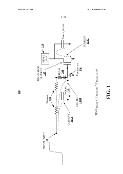
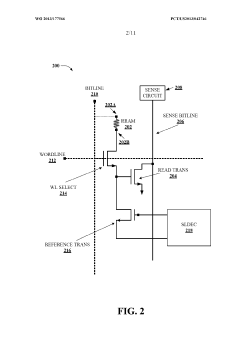
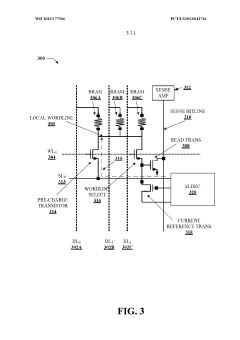
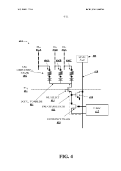
- The development of a high-speed RRAM architecture that connects multiple RRAM devices to a single read transistor, utilizing a reference transistor to apply a bias voltage and mitigate off-current, and employing a sensing circuit to quickly detect changes in electrical characteristics, enabling fast programming, reading, and erasing operations while reducing the number of read transistors and associated circuitry.
Resistive random access memory device
PatentActiveUS20180040816A1
Innovation
- A metal oxide-based CBRAM memory cell is developed, incorporating a transition metal from groups 3, 4, 5, or 6 and a chalcogen element, with an interface layer that creates oxygen vacancies, facilitating the formation of conductive filaments and enhancing their retention by acting as a barrier against filament dissolution.
Standardization Efforts in ReRAM Protocols
The standardization landscape for Resistive RAM (ReRAM) protocols remains fragmented, with multiple industry bodies working to establish cohesive frameworks. The JEDEC Solid State Technology Association has been particularly active, developing JC-42.4 and JC-42.6 committees focused on non-volatile memory interfaces that increasingly incorporate ReRAM-specific considerations. These efforts aim to create unified electrical specifications, command sets, and physical interfaces that can accelerate ReRAM adoption across computing platforms.
The IEEE has contributed through its P1817 working group, which addresses standardized interfaces for emerging non-volatile memory technologies including ReRAM. This initiative focuses on creating protocol abstractions that allow ReRAM to integrate seamlessly with existing memory hierarchies while leveraging its unique characteristics such as low latency and bit-addressability.
Parallel to these efforts, the Storage Networking Industry Association (SNIA) has developed the Non-Volatile Memory Programming Model (NVMP) that provides a standardized software interface for persistent memory technologies. While not ReRAM-specific, this model creates critical abstraction layers that enable ReRAM to function within existing storage architectures while maintaining its performance advantages.
Industry consortiums have emerged as powerful forces in ReRAM standardization. The Open NAND Flash Interface (ONFI) Working Group has expanded its scope to include ReRAM interfaces, recognizing the technology's potential to complement or eventually replace NAND in certain applications. Similarly, the MIPI Alliance has begun exploring ReRAM-specific protocols for mobile and IoT applications where power efficiency is paramount.
Challenges to standardization include the diversity of ReRAM materials systems (oxide-based, conductive-bridge, phase-change variants) and competing architectural approaches (crossbar arrays, 3D stacking, selector device integration). Each implementation presents unique electrical characteristics that complicate the development of universal protocols.
Regional standardization bodies have also entered the arena, with China's Electronics Standardization Institute (CESI) and the European Telecommunications Standards Institute (ETSI) developing region-specific frameworks. This geographical diversification risks creating incompatible protocol ecosystems unless international coordination improves.
The timeline for mature ReRAM protocol standardization remains uncertain, with most industry analysts projecting 2-3 years before comprehensive standards emerge. This standardization gap represents both a challenge for immediate deployment and an opportunity for companies willing to contribute to protocol development.
Power Efficiency Considerations for ReRAM Interfaces
Power efficiency has emerged as a critical consideration in the development of Resistive RAM (ReRAM) interfaces, particularly as these memory technologies gain traction in energy-constrained applications such as IoT devices, mobile systems, and edge computing. The fundamental power characteristics of ReRAM present both advantages and challenges when designing efficient interface protocols.
ReRAM's non-volatile nature offers inherent power advantages, as it maintains stored data without requiring refresh operations, unlike DRAM. This characteristic significantly reduces standby power consumption, making ReRAM particularly attractive for intermittently powered systems. However, the write operations in ReRAM can be power-intensive, requiring careful management through interface design to optimize overall system efficiency.
Current ReRAM interfaces typically implement several power-saving techniques. Voltage scaling during read operations has proven effective, as ReRAM cells can often be read reliably at lower voltages than those required for writing. Advanced interfaces now incorporate adaptive voltage control systems that dynamically adjust operating voltages based on cell characteristics and operation types.
Burst-mode operations represent another significant power optimization strategy. By grouping multiple read or write operations together, the power overhead associated with interface initialization can be amortized across multiple memory accesses. Modern ReRAM interfaces increasingly support configurable burst lengths to balance throughput requirements against power constraints.
Power gating techniques have been implemented in recent ReRAM interface designs, allowing unused circuit blocks to be completely disconnected from power supplies during idle periods. This approach is particularly effective for ReRAM due to its non-volatile nature, as data persistence is maintained even when power is removed from peripheral circuitry.
Temperature-aware operation represents an emerging consideration in ReRAM interface design. As ReRAM switching characteristics can vary with temperature, adaptive interfaces that adjust timing parameters and operating voltages based on thermal conditions can maintain optimal power efficiency across varying environmental conditions.
The trade-off between access speed and power consumption remains a central challenge. While faster switching times can be achieved through higher operating voltages, this approach significantly increases power consumption. Advanced ReRAM interfaces now implement multiple operating modes that allow systems to select appropriate speed-power trade-offs based on application requirements.
Looking forward, the integration of on-chip power monitoring and management systems directly into ReRAM interfaces presents a promising direction for further efficiency improvements. Such systems could enable real-time optimization of operating parameters based on actual device characteristics and workload patterns.
Unlock deeper insights with PatSnap Eureka Quick Research — get a full tech report to explore trends and direct your research. Try now!
Generate Your Research Report Instantly with AI Agent
Supercharge your innovation with PatSnap Eureka AI Agent Platform!