Exploration of the Resistive RAM Market by Application Domains
OCT 9, 20259 MIN READ
Generate Your Research Report Instantly with AI Agent
Patsnap Eureka helps you evaluate technical feasibility & market potential.
ReRAM Technology Background and Objectives
Resistive Random Access Memory (ReRAM) represents a revolutionary non-volatile memory technology that has evolved significantly over the past two decades. Initially conceptualized in the early 2000s, ReRAM emerged as a promising alternative to conventional memory technologies due to its unique ability to store information through changes in resistance states rather than electric charge. This fundamental operating principle enables ReRAM to overcome many limitations inherent in traditional memory architectures.
The evolution of ReRAM technology has been marked by several significant milestones. Early research focused primarily on understanding the resistance switching mechanisms in various metal oxide materials. By the mid-2000s, researchers had demonstrated functional ReRAM cells with promising performance characteristics. The period between 2010 and 2015 saw substantial improvements in endurance, retention, and switching speed, making ReRAM increasingly viable for commercial applications.
Current technological trends in the ReRAM landscape include the development of multi-level cell capabilities, which significantly enhance storage density, and the integration of ReRAM with conventional CMOS technology to create hybrid memory systems. Additionally, there is growing interest in leveraging ReRAM for neuromorphic computing applications, where its analog resistance states can effectively mimic synaptic behavior.
The primary technical objectives for ReRAM development include achieving higher density storage while maintaining reliability, reducing power consumption during write operations, and enhancing endurance to compete with established memory technologies. Researchers aim to reach write endurance exceeding 10^12 cycles, data retention periods of over 10 years, and switching speeds in the nanosecond range.
Another critical objective is scaling ReRAM technology to advanced process nodes below 10nm while preserving its performance advantages. This miniaturization is essential for enabling higher capacity memory arrays and facilitating integration with leading-edge logic processes. Simultaneously, efforts are underway to develop innovative materials and device structures that can improve the consistency of resistance switching and reduce variability between cells.
From an application perspective, ReRAM technology aims to address the growing demand for high-performance, energy-efficient memory solutions across various domains. These include edge computing devices requiring persistent memory with minimal power consumption, data centers seeking faster storage alternatives, and emerging AI applications that benefit from in-memory computing capabilities.
Market Demand Analysis for ReRAM Solutions
The global market for Resistive Random Access Memory (ReRAM) solutions is experiencing significant growth driven by increasing demands for advanced memory technologies across multiple application domains. Current market analysis indicates that the ReRAM market is projected to grow at a compound annual growth rate of 16% through 2028, with the market value expected to reach $2.4 billion by that time.
Consumer electronics represents the largest application segment for ReRAM technology, accounting for approximately 38% of the total market share. This dominance stems from the growing need for low-power, high-speed memory solutions in smartphones, tablets, and wearable devices. The consumer demand for longer battery life and faster data processing capabilities has positioned ReRAM as an attractive alternative to traditional memory technologies.
Enterprise storage systems constitute the second-largest market segment, representing about 27% of ReRAM applications. Data centers and cloud service providers are increasingly adopting ReRAM solutions to address the challenges of managing massive data volumes while reducing power consumption. The non-volatile nature of ReRAM, combined with its high endurance and fast write speeds, makes it particularly suitable for enterprise storage applications where data persistence and energy efficiency are critical requirements.
The automotive sector is emerging as a rapidly growing application domain for ReRAM technology, currently holding about 18% of the market share. Advanced driver-assistance systems (ADAS) and autonomous vehicles require robust memory solutions capable of operating reliably in extreme conditions. ReRAM's radiation hardness, temperature stability, and fast read/write capabilities align well with these demanding requirements.
Industrial IoT applications account for approximately 12% of the ReRAM market. The deployment of edge computing devices in industrial environments necessitates memory solutions with low power consumption and high reliability. ReRAM's ability to retain data without power and its resistance to environmental factors make it well-suited for industrial applications where maintenance access may be limited.
Healthcare and medical devices represent a smaller but growing segment at 5% of the market. The unique requirements of medical applications, including long-term data retention, security, and reliability, are driving interest in ReRAM solutions for implantable devices, patient monitoring systems, and medical imaging equipment.
Market research indicates that North America currently leads in ReRAM adoption with 42% market share, followed by Asia-Pacific at 38% and Europe at 20%. However, the Asia-Pacific region is expected to demonstrate the highest growth rate over the next five years due to increasing investments in semiconductor manufacturing and the rapid expansion of consumer electronics production.
ReRAM Development Status and Technical Challenges
Resistive RAM (ReRAM) technology has evolved significantly over the past decade, yet still faces several critical technical challenges that impede its widespread commercial adoption. Currently, ReRAM development stands at a crucial juncture where laboratory success has been demonstrated, but mass production challenges persist. The technology has reached manufacturing readiness levels (MRL) of 7-8 for select applications, with companies like Weebit Nano, Crossbar, and Fujitsu leading commercial implementations.
The primary technical challenge facing ReRAM development is reliability. Current devices suffer from inconsistent switching behavior, with cycle-to-cycle and device-to-device variations that can exceed 20% in resistance states. This variability significantly impacts data retention and read accuracy, particularly in multi-level cell configurations where precise resistance differentiation is essential.
Endurance limitations represent another significant hurdle. While NAND flash typically achieves 10^4-10^5 write cycles, and DRAM exceeds 10^16 cycles, most ReRAM implementations currently demonstrate only 10^6-10^9 cycles before performance degradation. This restricts ReRAM's applicability in write-intensive applications despite its theoretical potential for higher endurance.
The scaling challenge remains particularly problematic for ReRAM commercialization. As device dimensions shrink below 20nm, current leakage and resistance drift become more pronounced, compromising data integrity. Additionally, the integration of ReRAM with standard CMOS processes introduces materials compatibility issues, particularly regarding thermal budgets and contamination risks during fabrication.
Power consumption during the SET operation (transitioning from high to low resistance) requires relatively high current densities, typically 10^5-10^6 A/cm², which can cause localized heating and accelerate device degradation. This power requirement contradicts ReRAM's positioning as an energy-efficient memory solution, especially for edge computing and IoT applications.
From a manufacturing perspective, yield rates remain below optimal levels. Current production processes achieve approximately 85-90% yield for single-layer ReRAM, significantly lower than the 95%+ standard for mature memory technologies. This yield challenge becomes exponentially more difficult when implementing 3D crossbar architectures necessary for high-density storage applications.
The absence of standardized testing protocols and performance metrics further complicates ReRAM development. Unlike established memory technologies with well-defined benchmarking standards, ReRAM evaluation varies across research groups and manufacturers, making direct comparisons and quality assessments difficult for potential adopters and investors.
Current ReRAM Implementation Approaches
01 Resistive RAM device structures
Resistive RAM (RRAM) devices are typically structured with a resistive switching material sandwiched between two electrodes. Various device architectures have been developed, including crossbar arrays, 3D stacking configurations, and integration with transistors for improved performance. These structures aim to optimize memory density, reduce power consumption, and enhance switching reliability. The resistive switching layer can be composed of various materials that exhibit controllable resistance changes under applied voltage.- Materials and structures for resistive RAM: Various materials and structures are used in resistive RAM devices to achieve optimal performance. These include metal oxides, chalcogenides, and perovskites that exhibit resistive switching behavior. The structure typically consists of a switching layer sandwiched between two electrodes. Different configurations such as crossbar arrays and 3D stacking are employed to increase memory density and improve integration with CMOS technology.
- Resistive switching mechanisms: Resistive RAM operates based on different switching mechanisms that change the resistance state of the memory cell. These mechanisms include filamentary conduction, where conductive filaments form and rupture within the switching layer, and interface-type switching, where the resistance change occurs at the interface between the electrode and the switching material. Understanding these mechanisms is crucial for designing reliable and efficient resistive memory devices.
- Integration and fabrication techniques: Advanced fabrication techniques are essential for integrating resistive RAM into existing semiconductor technology. These include atomic layer deposition, physical vapor deposition, and various etching processes to create nanoscale memory cells. Back-end-of-line integration approaches allow resistive RAM to be stacked above conventional CMOS circuits, enabling high-density memory solutions with minimal impact on chip area.
- Operation and control circuits: Specialized circuits are required for the reliable operation of resistive RAM, including programming, reading, and erasing functions. These circuits control the voltage and current applied to memory cells to switch between high and low resistance states. Pulse shaping techniques and current compliance methods are employed to prevent device degradation and improve endurance. Sensing amplifiers with high sensitivity are used to detect the resistance state during read operations.
- Reliability and performance enhancement: Various approaches are used to enhance the reliability and performance of resistive RAM. These include doping the switching layer, engineering the electrode materials, and optimizing the programming conditions. Multi-level cell operation allows storing multiple bits per cell by utilizing intermediate resistance states. Techniques to mitigate variability, reduce power consumption, and improve retention time are critical for commercial viability of resistive RAM technology.
02 Resistive switching materials
The choice of resistive switching materials is crucial for RRAM performance. Common materials include metal oxides (such as HfOx, TaOx, TiOx), chalcogenides, and perovskites. These materials exhibit filamentary or interface-type switching mechanisms where conductive paths form and rupture to create high and low resistance states. Material engineering focuses on controlling defect concentration, oxygen vacancy distribution, and interface properties to achieve reliable switching behavior with high on/off ratios and long retention times.Expand Specific Solutions03 Operation and control mechanisms
RRAM operation involves SET and RESET processes that switch the device between low and high resistance states. Various control mechanisms have been developed to improve switching reliability and reduce variability, including current compliance techniques, pulse engineering, and multi-level programming schemes. Advanced operation methods include self-compliance designs, adaptive programming algorithms, and temperature-controlled switching to enhance endurance and retention characteristics while minimizing power consumption during write operations.Expand Specific Solutions04 Integration with CMOS technology
Integration of RRAM with conventional CMOS technology is essential for practical applications. This includes developing RRAM-compatible fabrication processes, addressing thermal budget constraints, and designing peripheral circuits for read/write operations. Back-end-of-line integration approaches allow RRAM cells to be fabricated in the metal interconnect layers above the silicon substrate, enabling 3D memory architectures without increasing chip area. Circuit designs must address issues like sneak path currents in crossbar arrays and provide sufficient sensing margins.Expand Specific Solutions05 Applications and emerging uses
Beyond conventional memory applications, RRAM is being explored for neuromorphic computing, in-memory computing, and security applications. The analog switching characteristics of RRAM make it suitable for implementing artificial synapses in neural networks. Other applications include non-volatile logic, reconfigurable computing architectures, and physical unclonable functions for hardware security. RRAM's low power consumption, high density, and CMOS compatibility make it promising for edge computing devices and Internet of Things applications where energy efficiency is critical.Expand Specific Solutions
Key Industry Players in ReRAM Market
The Resistive RAM (ReRAM) market is evolving rapidly across diverse application domains, currently transitioning from early commercialization to broader market adoption. With projected growth reaching $4-5 billion by 2025, ReRAM is gaining traction in IoT, automotive, and enterprise storage sectors. Leading semiconductor manufacturers including Micron Technology, Samsung Electronics, and SK hynix are advancing commercial ReRAM solutions, while specialized players like Winbond Electronics and Adesto Technologies focus on embedded applications. Research institutions such as ITRI and universities (Peking, Fudan) collaborate with foundries like TSMC and GlobalFoundries to overcome technical challenges in scalability and reliability. The technology's maturity varies by application, with consumer electronics implementations more advanced than emerging neuromorphic computing applications, which remain predominantly in research phases.
Micron Technology, Inc.
Technical Solution: Micron has developed advanced 3D ReRAM technology that combines high-density storage capabilities with CMOS logic integration. Their solution employs a cross-point architecture where memory cells are positioned at the intersection of word and bit lines, enabling ultra-high density storage. Micron's ReRAM technology utilizes metal-oxide switching materials that change resistance states when voltage is applied, creating a non-volatile memory solution. Their implementation focuses on embedded applications requiring both high performance and low power consumption, with particular emphasis on edge AI computing and IoT devices. Micron has demonstrated ReRAM arrays with sub-10ns switching speeds and endurance exceeding 10^6 cycles, positioning their technology as a viable alternative to both NAND flash and DRAM in specific application domains.
Strengths: Superior switching speed (sub-10ns) compared to NAND flash; excellent power efficiency for IoT applications; high endurance suitable for frequently updated data. Weaknesses: Higher cost per bit compared to NAND flash; scaling challenges below certain process nodes; requires specialized interface circuits.
Adesto Technologies Corp.
Technical Solution: Adesto has developed a specialized ReRAM technology called CBRAM (Conductive Bridging RAM) that utilizes electrochemical metallization cells. Their approach employs a solid electrolyte layer between active metal and inert electrodes, where applying voltage creates or dissolves conductive metal filaments. Adesto's ReRAM solutions primarily target ultra-low power IoT and embedded applications, with particular focus on battery-operated and energy harvesting systems. Their technology operates at voltages as low as 1.2V and consumes approximately 100x less energy for write operations compared to conventional embedded flash. Adesto has successfully commercialized their ReRAM technology in products like the EcoXiP and DataFlash series, which serve applications ranging from wearable devices to industrial sensors. Their implementation achieves write speeds of approximately 50μs with retention exceeding 10 years and endurance of 100,000 cycles, making it particularly suitable for applications requiring frequent small updates with minimal power consumption.
Strengths: Ultra-low power consumption ideal for battery-powered devices; commercially deployed in multiple product lines; excellent retention characteristics. Weaknesses: Lower density compared to leading NAND flash; more limited ecosystem support; slower write speeds compared to some competing ReRAM technologies.
Critical ReRAM Patents and Technical Innovations
Resistive random access memory and verifying method thereof
PatentActiveUS8300449B2
Innovation
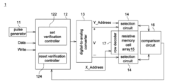
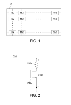
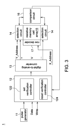
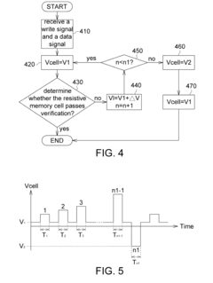
- The implementation of a resistive random access memory (RRAM) system that includes a resistive memory cell, a digital-to-analog converter, a decision logic, and a selection circuit, which applies a reverse voltage to the resistive memory cell during verification failures, utilizing a reference voltage and voltage pulses to enhance the verification process.
ReRAM Application Domain Segmentation
The ReRAM market demonstrates distinct segmentation across various application domains, each leveraging the unique advantages of this emerging non-volatile memory technology. Consumer electronics represents the largest current market segment, with ReRAM being integrated into smartphones, tablets, and wearable devices to enable faster boot times, improved energy efficiency, and enhanced user experiences through persistent memory capabilities.
Enterprise storage systems constitute another significant domain, where ReRAM's combination of DRAM-like speed and flash-like non-volatility positions it as an ideal solution for high-performance computing environments. Data centers are increasingly adopting ReRAM-based solutions to address the growing demands of real-time data processing and analytics, particularly for applications requiring low latency and high throughput.
The automotive sector presents a rapidly expanding opportunity for ReRAM deployment, particularly in advanced driver-assistance systems (ADAS) and autonomous vehicles. These applications benefit from ReRAM's radiation hardness, wide temperature operation range, and fast read/write capabilities, which are essential for processing sensor data in real-time driving scenarios.
Industrial IoT represents another promising domain, with ReRAM enabling edge computing devices to perform complex data processing tasks with minimal power consumption. The technology's ability to retain data without power makes it particularly valuable for remote or battery-powered IoT deployments in manufacturing, agriculture, and smart infrastructure applications.
Healthcare and medical devices are emerging as specialized application domains for ReRAM, where its reliability and radiation resistance make it suitable for implantable devices and medical imaging equipment. The technology's low power consumption extends battery life in portable medical devices, while its fast operation supports real-time monitoring and diagnostic applications.
Aerospace and defense applications leverage ReRAM's inherent radiation hardness and reliability in extreme environments. Satellite systems, military equipment, and avionics benefit from ReRAM's ability to maintain data integrity under challenging conditions, including radiation exposure and temperature fluctuations.
AI and machine learning acceleration represents perhaps the most promising future growth domain for ReRAM. The technology's ability to perform in-memory computing makes it particularly well-suited for neural network implementations, potentially reducing power consumption by orders of magnitude compared to conventional von Neumann architectures when executing AI workloads.
Supply Chain Analysis for ReRAM Manufacturing
The ReRAM manufacturing supply chain represents a complex ecosystem involving multiple stakeholders across various geographical regions. Material suppliers form the foundation of this chain, providing specialized materials such as metal oxides (HfO2, TiO2), electrode materials (Pt, TiN), and various dopants essential for ReRAM functionality. These suppliers are predominantly located in East Asia, North America, and Europe, with companies like Tokyo Electron and Applied Materials playing significant roles.
Fabrication equipment manufacturers constitute another critical segment, developing specialized tools for atomic layer deposition, physical vapor deposition, and etching processes required for ReRAM production. The equipment market is dominated by established semiconductor equipment providers who have expanded their portfolios to accommodate emerging memory technologies.
Foundry services represent a pivotal component in the ReRAM supply chain. Major semiconductor foundries like TSMC, GlobalFoundries, and UMC have developed specialized processes for ReRAM integration, offering both standalone ReRAM solutions and embedded ReRAM options integrated with CMOS logic. This segment faces challenges in scaling production while maintaining consistent switching characteristics across wafers.
Integration and packaging services handle the final stages of production, with companies specializing in advanced packaging techniques suitable for ReRAM's unique requirements. These services are concentrated in Taiwan, South Korea, and China, leveraging existing semiconductor packaging infrastructure.
The supply chain faces several bottlenecks, including limited material standardization, process variability challenges, and equipment specialization requirements. Material consistency remains a significant concern, as minor variations can dramatically affect ReRAM performance characteristics. Additionally, the industry confronts scaling challenges as it transitions from research-scale to mass production volumes.
Geopolitical factors increasingly influence the ReRAM supply chain, with national security concerns driving reshoring initiatives in the US and Europe. Meanwhile, China is heavily investing in domestic memory production capabilities to reduce dependency on foreign technologies. These dynamics create both challenges and opportunities for supply chain diversification and resilience building.
Cost structures within the ReRAM manufacturing ecosystem remain higher than established memory technologies, primarily due to specialized material requirements and lower production volumes. However, as adoption increases across application domains, economies of scale are expected to gradually improve cost competitiveness against incumbent technologies.
Unlock deeper insights with Patsnap Eureka Quick Research — get a full tech report to explore trends and direct your research. Try now!
Generate Your Research Report Instantly with AI Agent
Supercharge your innovation with Patsnap Eureka AI Agent Platform!