Resistive RAM Applications: Industry Analysis and Projections
OCT 9, 20259 MIN READ
Generate Your Research Report Instantly with AI Agent
Patsnap Eureka helps you evaluate technical feasibility & market potential.
ReRAM Technology Background and Objectives
Resistive Random Access Memory (ReRAM) represents a significant advancement in non-volatile memory technology, emerging as a promising alternative to conventional memory solutions. The evolution of ReRAM can be traced back to the early 2000s when researchers began exploring the potential of resistance switching phenomena in various metal oxide materials. This technology leverages the ability to reversibly change the resistance state of a dielectric material, enabling data storage through resistance variations rather than electrical charge.
The development trajectory of ReRAM has been characterized by progressive improvements in material science, fabrication techniques, and device architecture. Initially hindered by reliability issues and manufacturing complexities, recent breakthroughs in nanoscale fabrication and material engineering have substantially enhanced ReRAM's performance metrics, including endurance, retention time, and switching speed.
Current technological trends indicate a growing convergence between memory and computing functionalities, with ReRAM positioned at the intersection of this paradigm shift. The inherent characteristics of ReRAM—low power consumption, high density, and non-volatility—align well with the demands of emerging computing paradigms such as neuromorphic computing and in-memory processing.
The primary technical objectives for ReRAM development encompass several dimensions. First, enhancing scalability to achieve higher storage densities while maintaining reliability at reduced feature sizes. Second, improving switching uniformity and reducing variability across devices to ensure consistent performance. Third, extending endurance capabilities to support applications requiring frequent write operations.
Additionally, researchers aim to optimize the energy efficiency of ReRAM operations, particularly focusing on reducing the current required for resistance switching. This objective is crucial for enabling ReRAM's integration into energy-constrained applications such as IoT devices and mobile systems.
From a manufacturing perspective, a key goal involves developing fabrication processes compatible with standard CMOS technology, facilitating seamless integration with existing semiconductor manufacturing infrastructure. This compatibility would significantly accelerate commercial adoption and reduce production costs.
The long-term vision for ReRAM technology extends beyond conventional memory applications. Researchers are exploring its potential as a fundamental building block for novel computing architectures, particularly those mimicking neurological processes. The ability of ReRAM to emulate synaptic behavior makes it an ideal candidate for implementing artificial neural networks directly in hardware, potentially revolutionizing approaches to artificial intelligence and machine learning.
As the technology continues to mature, the focus increasingly shifts toward addressing system-level integration challenges and developing standardized interfaces that enable ReRAM to function effectively within diverse computing environments.
Market Demand Analysis for ReRAM Solutions
The global market for Resistive Random Access Memory (ReRAM) solutions is experiencing significant growth, driven by increasing demands for advanced memory technologies that overcome the limitations of conventional memory systems. Current market analysis indicates that the ReRAM market is projected to grow at a compound annual growth rate of 16% through 2028, with the market value expected to reach approximately $1.2 billion by that time.
The primary demand drivers for ReRAM technology stem from several key industries. The consumer electronics sector represents the largest market segment, with smartphone manufacturers increasingly interested in ReRAM's potential to reduce power consumption while improving data retention capabilities. This sector's demand is particularly strong in regions with high smartphone penetration rates such as North America, Europe, and East Asia.
Enterprise storage systems constitute another significant market segment, where the need for faster, more reliable non-volatile memory solutions continues to grow exponentially with the expansion of cloud computing and big data applications. Data centers are actively seeking memory technologies that can reduce latency and power consumption while maintaining data integrity, making ReRAM an attractive alternative to traditional flash memory.
The automotive industry represents an emerging but rapidly growing market for ReRAM solutions. As vehicles become more sophisticated with advanced driver-assistance systems (ADAS) and autonomous driving capabilities, the demand for high-performance, reliable memory that can withstand extreme operating conditions has increased substantially. ReRAM's radiation hardness and temperature stability make it particularly suitable for automotive applications.
Internet of Things (IoT) devices present perhaps the most promising long-term growth opportunity for ReRAM technology. The projected deployment of billions of connected devices requires memory solutions that combine low power consumption, small form factor, and sufficient durability to operate for years without maintenance. Market research indicates that IoT applications could account for up to 30% of the total ReRAM market by 2030.
From a geographical perspective, the Asia-Pacific region currently dominates the ReRAM market, accounting for approximately 45% of global demand. This is largely attributable to the concentration of semiconductor manufacturing facilities and consumer electronics production in countries like South Korea, Japan, Taiwan, and China. North America follows with roughly 30% market share, driven primarily by data center applications and military/aerospace requirements.
The market demand analysis also reveals significant interest from specialized sectors including aerospace, military, and medical devices, where ReRAM's radiation hardness and non-volatility provide critical advantages over conventional memory technologies. These niche markets, while smaller in volume, often command premium pricing and represent high-margin opportunities for ReRAM manufacturers.
ReRAM Technical Status and Challenges
Resistive RAM (ReRAM) technology has reached a critical juncture in its development cycle, with significant advancements achieved in recent years but still facing substantial challenges before widespread commercial adoption. Currently, ReRAM devices demonstrate promising characteristics including low power consumption, high switching speed, and excellent scalability compared to conventional memory technologies. Laboratory demonstrations have achieved switching speeds below 10ns and endurance cycles exceeding 10^12, positioning ReRAM as a viable candidate for next-generation non-volatile memory applications.
The global landscape of ReRAM development shows concentration in three major regions: North America, East Asia (particularly Japan, South Korea, and Taiwan), and Europe. Each region exhibits distinct research focuses, with North American institutions emphasizing novel materials and architectures, Asian companies prioritizing manufacturing scalability, and European research centers focusing on reliability and specialized applications.
Despite impressive progress, ReRAM faces several significant technical challenges. Retention reliability remains problematic, with data degradation occurring over time due to oxygen vacancy migration even at room temperature. This issue becomes more pronounced as device dimensions shrink below 20nm. Variability between devices and cycle-to-cycle inconsistency presents another major hurdle, complicating circuit design and potentially requiring sophisticated error correction mechanisms.
The sneak path current problem in crossbar arrays continues to limit array size and density, though selector devices and complementary resistive switching approaches offer promising but incomplete solutions. Material stability represents another critical challenge, as the complex metal oxide structures used in many ReRAM designs can undergo undesirable phase transformations during operation, affecting long-term reliability.
Manufacturing integration with standard CMOS processes presents significant difficulties, particularly regarding thermal budget compatibility and contamination concerns. The industry has made progress in addressing these issues, but full compatibility remains elusive, especially for advanced process nodes below 28nm.
Scaling challenges become increasingly prominent as dimensions approach sub-10nm, where quantum effects and material constraints fundamentally alter device behavior. Research groups have demonstrated functioning devices at 5nm, but reproducibility and performance consistency remain problematic at these dimensions.
The read/write energy efficiency of ReRAM, while superior to many competing technologies, still requires improvement for ultra-low-power applications such as IoT edge devices and implantable medical systems. Current designs typically require 1-10 pJ per operation, whereas theoretical limits suggest sub-femtojoule operation might be achievable with optimized materials and architectures.
Current ReRAM Implementation Approaches
01 Resistive RAM device structures
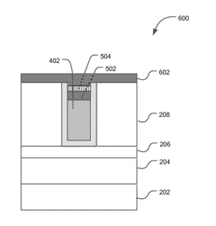
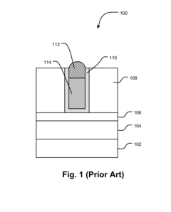
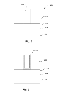
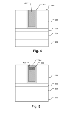
Resistive RAM (RRAM) devices are constructed with specific structural configurations to optimize performance. These structures typically include a resistive switching layer sandwiched between two electrodes. Various materials can be used for the resistive layer, including metal oxides, chalcogenides, and perovskites. The electrode materials and their interfaces with the resistive layer play crucial roles in determining switching characteristics. Advanced structures may incorporate additional layers for improved stability, retention, and endurance.- Materials and structures for RRAM devices: Resistive Random Access Memory (RRAM) devices utilize specific materials and structures to enable resistive switching behavior. These typically include metal oxides like HfO2, TiO2, or Ta2O5 as the switching layer sandwiched between two electrodes. The structure may incorporate additional layers such as barrier layers or doping elements to enhance performance. The arrangement of these materials in specific configurations allows for the formation and rupture of conductive filaments that enable the switching between high and low resistance states.
- Switching mechanisms and operation principles: RRAM devices operate based on resistive switching mechanisms where the resistance of the memory cell can be altered between high and low states. This switching behavior typically relies on the formation and dissolution of conductive filaments within the insulating layer, often through ion migration or redox processes. The operation involves SET operations (switching to low resistance state) and RESET operations (returning to high resistance state) controlled by applied voltage or current. Understanding these mechanisms is crucial for optimizing device performance and reliability.
- Integration and fabrication techniques: Fabrication of RRAM devices involves specialized integration techniques compatible with semiconductor manufacturing processes. These include deposition methods for the resistive switching layer such as atomic layer deposition, sputtering, or chemical vapor deposition. The fabrication process may involve precise control of layer thicknesses, interface engineering, and thermal treatments to optimize device characteristics. Integration challenges include ensuring compatibility with CMOS processes, minimizing cell size, and developing 3D stacking approaches for higher density memory arrays.
- Circuit design and memory architecture: RRAM memory architecture involves specific circuit designs to address, read, write, and erase memory cells. These architectures may include crossbar arrays, selector devices to prevent sneak path currents, and peripheral circuits for sensing and programming operations. The circuit design must account for the unique electrical characteristics of RRAM cells, including nonlinear current-voltage behavior and resistance variations. Advanced architectures may incorporate multi-level cell capabilities, enabling storage of multiple bits per cell through distinct resistance states.
- Performance enhancement and reliability solutions: Improving RRAM performance and reliability involves addressing challenges such as resistance drift, endurance limitations, and variability between cells. Solutions include material engineering approaches like doping or interface modification, optimized programming schemes to reduce stress on the devices, and error correction techniques. Other enhancements focus on reducing operating power, improving switching speed, and extending retention time. These improvements are essential for enabling RRAM to compete with established memory technologies in various applications from embedded systems to storage class memory.
02 Resistive switching mechanisms
The operation of resistive RAM relies on various switching mechanisms that change the resistance state of the memory cell. These mechanisms include filamentary conduction, where conductive filaments form and rupture within the resistive layer, and interface-type switching, where the resistance changes at the electrode-oxide interface. Other mechanisms involve oxygen vacancy migration, ion migration, or phase changes in the resistive material. Understanding these mechanisms is essential for designing reliable RRAM devices with consistent switching behavior and long-term stability.Expand Specific Solutions03 Material innovations for RRAM
Material selection and engineering are critical aspects of resistive RAM development. Various materials are being explored for the resistive switching layer, including transition metal oxides (HfOx, TaOx, TiOx), chalcogenides, and complex oxides. Electrode materials range from noble metals to conductive nitrides and oxides. Doping strategies and interface engineering are employed to enhance switching characteristics, reduce variability, and improve retention. Novel two-dimensional materials and nanocomposites are also being investigated to achieve higher performance and scalability.Expand Specific Solutions04 Integration and fabrication techniques
Successful implementation of resistive RAM technology depends on effective integration and fabrication techniques. These include methods for depositing uniform thin films, patterning nanoscale features, and ensuring compatibility with CMOS processes. Advanced techniques such as atomic layer deposition, reactive sputtering, and solution processing are employed to create high-quality resistive layers. 3D integration approaches, such as crossbar arrays and vertical stacking, enable high-density memory architectures. Post-fabrication treatments like thermal annealing and electrical forming are often used to optimize device performance.Expand Specific Solutions05 Circuit design and operation schemes
Circuit design plays a crucial role in addressing the challenges of resistive RAM operation, including sneak path issues, read/write disturbances, and variability. Various selector devices and array architectures are implemented to enable reliable operation of large RRAM arrays. Programming schemes with precise voltage/current control are developed to achieve consistent switching behavior. Sensing circuits are designed to accurately detect the resistance states while minimizing power consumption. Advanced error correction codes and redundancy schemes are employed to enhance reliability and extend the lifetime of RRAM-based memory systems.Expand Specific Solutions
Key Industry Players in ReRAM Development
The Resistive RAM (ReRAM) market is currently in a growth phase, transitioning from early adoption to broader commercialization. The global market size is projected to reach approximately $4-5 billion by 2026, with a CAGR of 30-35%. Leading semiconductor manufacturers including Samsung, Micron, and KIOXIA are advancing ReRAM technology alongside specialized players like CrossBar and Adesto Technologies. IBM, Intel, and SK hynix are investing heavily in R&D to overcome technical challenges in scalability and endurance. The technology has reached moderate maturity for specific applications but requires further development for mainstream adoption. Asian manufacturers, particularly from Taiwan (Winbond, Macronix) and South Korea, dominate production capacity, while research institutions like ITRI and universities continue to drive fundamental innovation in materials and architectures.
International Business Machines Corp.
Technical Solution: IBM has pioneered phase-change memory (PCM) technology as their primary ReRAM implementation, utilizing chalcogenide materials (typically germanium-antimony-tellurium compounds) that switch between amorphous and crystalline states. Their technology demonstrates multi-level cell capabilities with up to 3 bits per cell, achieved through precise current control during programming. IBM's ReRAM shows read latencies of approximately 75ns and write operations in the 150-300ns range, positioning it between DRAM and flash in the memory hierarchy. The company has demonstrated reliable operation for over 10^7 cycles and data retention exceeding 10 years at operating temperatures. IBM's unique contribution includes the development of projected PCM (PPCM) technology, which reduces the contact area between the heater and phase-change material, significantly improving energy efficiency. Their research has particularly focused on neuromorphic applications, where analog resistance states can implement synaptic weights for AI acceleration, demonstrating energy efficiencies below 1pJ per synaptic operation in their prototype neural network accelerators.
Strengths: Industry-leading research in materials science and device physics; strong focus on system-level integration and neuromorphic applications; extensive patent portfolio covering fundamental ReRAM mechanisms. Weaknesses: Manufacturing complexity of phase-change materials may impact production costs; thermal management challenges in high-density arrays require sophisticated engineering solutions.
Micron Technology, Inc.
Technical Solution: Micron has developed a comprehensive ReRAM technology platform focused on embedded applications. Their 3D crosspoint architecture utilizes chalcogenide-based materials in a two-terminal memory cell structure that enables non-volatile storage without requiring a transistor at each cell. Micron's ReRAM technology demonstrates switching speeds in the nanosecond range, significantly outperforming NAND flash, while operating at lower voltages (2-3V) than competing technologies. The company has achieved working prototypes with endurance exceeding 1 million cycles and data retention of over 10 years at 85°C. Micron's manufacturing approach integrates ReRAM into their existing memory fabrication infrastructure, leveraging back-end-of-line (BEOL) processing that allows memory layers to be stacked above logic circuitry. This enables high-density storage solutions while maintaining compatibility with standard CMOS processes.
Strengths: Established manufacturing infrastructure allows for faster commercialization; strong IP portfolio in ReRAM materials and architectures; ability to integrate with existing memory product lines. Weaknesses: Faces competition from alternative emerging memory technologies within their own portfolio (including 3D XPoint); scaling challenges at advanced nodes require continuous materials engineering investment.
Critical ReRAM Patents and Technical Innovations
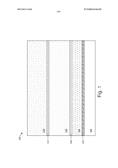
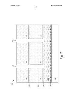
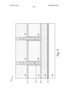
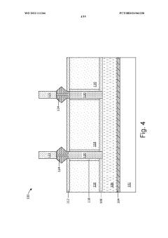
Resistive random access memory integrated with vertical transport field effect transistors
PatentWO2021111266A1
Innovation
- Integration of ReRAM with vertical transport field effect transistors (VTFETs) using the top source drain as the bottom electrode, with an oxide layer contacting the VTFETs, and forming the ReRAM in the facetted epitaxy drain region to enhance the electric field and control filament formation.
Resistive ram and fabrication method
PatentActiveUS20140264237A1
Innovation
- The method involves forming a nitrogen-containing metal oxide layer, such as tungsten oxynitride, over a transition metal electrode using a rapid thermal oxidation process, which reduces the forming voltage and improves the flatness of the metal oxide surface, facilitating subsequent processing and enhancing device performance by lowering the set and reset voltages.
ReRAM Manufacturing Processes and Scalability
ReRAM manufacturing has evolved significantly over the past decade, transitioning from laboratory prototypes to commercial production. Current manufacturing processes primarily utilize standard CMOS fabrication techniques, which has accelerated industry adoption by leveraging existing semiconductor infrastructure. The typical ReRAM cell structure consists of a metal-insulator-metal (MIM) stack, where the insulating layer—commonly metal oxides like HfOx, TaOx, or TiOx—serves as the switching medium.
The integration of ReRAM into the back-end-of-line (BEOL) process represents a significant manufacturing advantage, enabling 3D stacking capabilities without substantial modifications to front-end processes. This approach has been demonstrated by companies like Weebit Nano and Crossbar, who have successfully implemented ReRAM layers above conventional CMOS logic.
Scalability remains both a strength and challenge for ReRAM technology. On one hand, ReRAM cells can theoretically scale below 10nm, offering density advantages over conventional memory technologies. Several research institutions have demonstrated functional ReRAM cells at 5nm nodes, suggesting compatibility with advanced semiconductor roadmaps.
However, manufacturing challenges persist at these advanced nodes. Uniformity of switching behavior across large arrays represents a significant hurdle, as variations in the filament formation process can lead to reliability issues. Atomic Layer Deposition (ALD) has emerged as a preferred technique for depositing the critical oxide layer, providing better thickness control and uniformity compared to traditional sputtering methods.
Yield management presents another manufacturing challenge, particularly as array sizes increase. Current industrial production typically achieves yields of 85-90% for smaller arrays, but this decreases significantly for gigabit-scale memories. Leading manufacturers have implemented specialized testing and repair mechanisms, including redundancy schemes and adaptive programming algorithms, to mitigate these yield concerns.
Cost considerations remain central to ReRAM's commercial viability. While the basic cell structure is relatively simple, the specialized materials and precise control requirements add complexity to the manufacturing process. Industry analysis suggests that ReRAM manufacturing costs currently exceed those of established memory technologies like NAND flash on a per-bit basis, though this gap is expected to narrow as production volumes increase and processes mature.
Recent innovations in manufacturing include the development of multi-level cell (MLC) capabilities, where a single ReRAM cell can store multiple bits by utilizing intermediate resistance states. This approach potentially doubles or triples memory density without increasing manufacturing complexity proportionally, though it introduces additional challenges in resistance state control and read accuracy.
Energy Efficiency and Sustainability Aspects of ReRAM
Resistive RAM (ReRAM) technology offers significant advantages in energy efficiency compared to conventional memory technologies, positioning it as a sustainable alternative for future computing systems. The power consumption of ReRAM during operation is substantially lower than that of DRAM and NAND flash, with typical read operations consuming 10-100 times less energy than equivalent DRAM operations. This efficiency stems from ReRAM's fundamental operating principle, which requires energy only during state changes rather than for continuous state maintenance.
The manufacturing process of ReRAM also demonstrates environmental benefits. Production requires fewer mask layers and processing steps compared to conventional memory technologies, resulting in reduced material consumption and waste generation. Additionally, many ReRAM devices utilize abundant materials like silicon oxide and titanium oxide, avoiding the dependency on rare earth elements that characterize certain other emerging memory technologies.
From a lifecycle perspective, ReRAM devices exhibit excellent durability with endurance ratings reaching 10^12 cycles in laboratory settings, significantly outperforming NAND flash memory. This extended operational lifespan reduces electronic waste generation and the environmental impact associated with frequent device replacement.
When implemented in edge computing applications, ReRAM enables significant system-level energy savings. By allowing data processing directly within memory (compute-in-memory), ReRAM eliminates the energy-intensive data transfer between separate processing and storage units that accounts for up to 60% of energy consumption in conventional computing architectures. This capability is particularly valuable for IoT deployments, where energy constraints often limit functionality.
Several industry leaders have quantified these sustainability benefits. Crossbar Inc. reports that their ReRAM technology consumes approximately 20 times less power than equivalent NAND flash in standby mode. Similarly, Weebit Nano has demonstrated ReRAM cells that operate at voltages below 1V, further reducing power requirements compared to conventional technologies operating at 3-5V.
Looking forward, the integration of ReRAM in neuromorphic computing presents perhaps the most promising sustainability application. These brain-inspired computing systems leverage ReRAM's analog properties to perform complex AI operations at a fraction of the energy cost of digital implementations. Research from Stanford University suggests that ReRAM-based neuromorphic systems could potentially reduce energy consumption for certain AI workloads by up to three orders of magnitude compared to GPU-based solutions.
Unlock deeper insights with Patsnap Eureka Quick Research — get a full tech report to explore trends and direct your research. Try now!
Generate Your Research Report Instantly with AI Agent
Supercharge your innovation with Patsnap Eureka AI Agent Platform!