Standards and Compliance in Resistive RAM Industry
OCT 9, 202510 MIN READ
Generate Your Research Report Instantly with AI Agent
Patsnap Eureka helps you evaluate technical feasibility & market potential.
ReRAM Technology Background and Objectives
Resistive Random Access Memory (ReRAM) has emerged as a promising non-volatile memory technology over the past two decades, positioned as a potential successor to conventional memory technologies like DRAM and NAND flash. The evolution of ReRAM technology can be traced back to the early 2000s when researchers began exploring the resistive switching phenomena in various metal oxide materials. This technology leverages the ability of certain materials to change their resistance state when subjected to electrical stimuli, enabling data storage through resistance variations rather than electron charge.
The development trajectory of ReRAM has been characterized by significant advancements in material science, device architecture, and fabrication techniques. Early research focused primarily on understanding the fundamental switching mechanisms, while recent efforts have shifted toward addressing reliability, endurance, and scalability challenges. The technology has progressed from simple proof-of-concept devices to more sophisticated structures with improved performance metrics, including faster switching speeds, lower power consumption, and enhanced retention capabilities.
Industry standardization efforts for ReRAM began to take shape around 2010, with various semiconductor consortia and standards organizations recognizing the need for unified specifications to facilitate broader adoption. However, unlike established memory technologies, ReRAM standards remain in a relatively nascent stage, with fragmented approaches across different manufacturers and research institutions.
The primary technical objectives for ReRAM standardization include establishing uniform testing methodologies, defining performance benchmarks, ensuring interoperability between different implementations, and creating compliance frameworks that address reliability and endurance requirements. These standards aim to provide a common language for manufacturers, system integrators, and end-users, enabling more straightforward comparison and evaluation of different ReRAM solutions.
From a market perspective, ReRAM technology targets applications requiring non-volatility, high density, low power consumption, and fast access times. These include next-generation storage-class memory, embedded systems, Internet of Things (IoT) devices, and neuromorphic computing platforms. The technology's ability to bridge the performance gap between DRAM and NAND flash positions it as a compelling solution for emerging computing architectures that demand both speed and persistence.
Looking forward, the evolution of ReRAM standards is expected to follow a trajectory similar to other memory technologies, with initial focus on basic electrical specifications and testing procedures, gradually expanding to encompass more complex aspects such as reliability modeling, failure analysis methodologies, and integration guidelines for various system architectures. The establishment of comprehensive standards will be crucial for accelerating ReRAM's transition from research laboratories to mainstream commercial applications.
Market Demand Analysis for ReRAM Solutions
The global market for Resistive Random Access Memory (ReRAM) solutions is experiencing significant growth, driven by increasing demands for advanced non-volatile memory technologies that overcome the limitations of conventional memory architectures. Current market analysis indicates that the ReRAM sector is projected to grow at a compound annual growth rate of 16% through 2028, with particular acceleration in edge computing, Internet of Things (IoT), and artificial intelligence applications.
The primary market demand for ReRAM stems from its unique value proposition of low power consumption, high endurance, and fast switching speeds. These characteristics make it particularly attractive for battery-powered IoT devices where energy efficiency is paramount. Industry surveys reveal that approximately 40% of IoT device manufacturers are actively exploring ReRAM integration to extend device battery life and improve performance metrics.
Data center operators represent another significant market segment, with growing interest in ReRAM for in-memory computing applications. The technology's ability to perform computational tasks within the memory itself rather than transferring data to a separate processor addresses the increasing concerns about data movement energy costs, which currently account for up to 60% of total system energy in conventional architectures.
Automotive electronics manufacturers are emerging as a rapidly expanding market for ReRAM solutions, particularly for advanced driver-assistance systems (ADAS) and autonomous vehicles. These applications require memory technologies that can withstand extreme temperatures and radiation while maintaining data integrity. Market research indicates that automotive-grade ReRAM demand is growing twice as fast as the overall ReRAM market.
Consumer electronics remains the largest current market segment for ReRAM, with smartphone manufacturers integrating this technology to improve device performance and reduce power consumption. The demand is further amplified by the growing computational requirements of mobile applications, particularly those involving machine learning algorithms that benefit from ReRAM's parallel processing capabilities.
Geographic analysis reveals that Asia-Pacific dominates the ReRAM market demand, accounting for approximately 65% of global consumption, followed by North America at 20% and Europe at 12%. This distribution closely aligns with the regional concentration of semiconductor manufacturing facilities and consumer electronics production.
A significant market constraint identified in industry reports is the lack of standardized testing and qualification procedures for ReRAM technologies. This absence of unified standards creates uncertainty among potential adopters and slows market penetration. Consequently, there is growing demand for industry-wide compliance frameworks that would accelerate ReRAM adoption across various sectors by establishing clear reliability benchmarks and interoperability guidelines.
Current Standards Landscape and Technical Challenges
The Resistive RAM (ReRAM) industry currently faces a fragmented standards landscape, with no unified global framework specifically tailored for this emerging memory technology. Major semiconductor standards bodies including JEDEC, IEEE, and SEMI have established working groups addressing various aspects of non-volatile memory technologies, but comprehensive ReRAM-specific standards remain underdeveloped. This fragmentation creates significant challenges for manufacturers, integrators, and end-users seeking to implement ReRAM solutions at scale.
JEDEC's JC-42 Committee on Solid State Memories has developed standards for various memory technologies, but ReRAM-specific protocols are still evolving. Similarly, IEEE's 1801 and 1500 standards provide some applicable frameworks for testing and power management that ReRAM developers leverage, though these were not designed with ReRAM's unique characteristics in mind. The International Electrotechnical Commission (IEC) has begun addressing reliability testing methodologies that could be adapted for ReRAM, but dedicated standards remain limited.
The technical challenges stemming from this standards gap are multifaceted. First, interoperability issues persist across different manufacturers' ReRAM implementations, creating integration difficulties for system designers. Without standardized interfaces and protocols, each ReRAM solution effectively operates as a proprietary system, limiting broader adoption and increasing implementation costs.
Reliability assessment represents another critical challenge. The unique switching mechanisms and failure modes of ReRAM differ substantially from conventional memory technologies, requiring specialized testing methodologies. Current testing standards developed for NAND flash or DRAM cannot adequately characterize ReRAM's endurance, retention, and resistance drift characteristics, leading to inconsistent performance metrics across the industry.
Data security and integrity verification standards also lag behind ReRAM's technological capabilities. As ReRAM finds increasing applications in secure systems and IoT devices, the absence of standardized security protocols specifically addressing ReRAM's vulnerability profile creates potential security gaps. This is particularly concerning as ReRAM's non-volatile nature presents unique data remanence challenges not addressed in existing memory security frameworks.
Manufacturing process standardization represents perhaps the most significant hurdle. Current semiconductor fabrication standards do not fully address the specialized materials and processes required for ReRAM production. The diversity of materials systems used in ReRAM devices—ranging from oxide-based to chalcogenide-based structures—further complicates standardization efforts. This lack of process standardization contributes to yield inconsistencies and hampers cost reduction initiatives critical for mass market adoption.
Regulatory compliance frameworks across different regions add another layer of complexity. While general electronic component regulations apply to ReRAM devices, the technology's unique characteristics—particularly regarding data persistence and potential environmental impacts of novel materials—are not specifically addressed in current regulatory frameworks, creating uncertainty for global deployment strategies.
Current Compliance Frameworks and Implementation Approaches
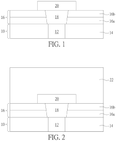
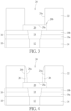
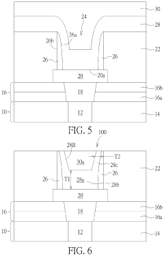
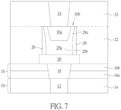
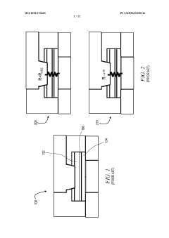
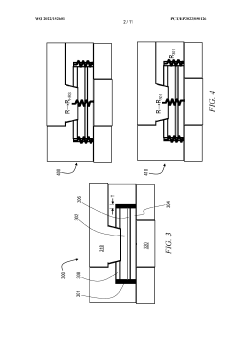
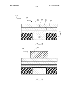
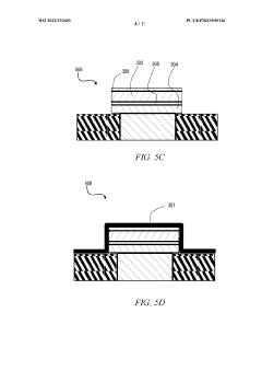
01 Resistive RAM structure and materials
Resistive RAM (RRAM) devices are structured with specific materials to enable resistive switching behavior. These typically include a metal-insulator-metal (MIM) configuration where the insulator layer can be made of various materials such as metal oxides, chalcogenides, or perovskites. The choice of materials affects key performance parameters like switching speed, endurance, and retention time. The resistive switching mechanism relies on the formation and rupture of conductive filaments within the insulator layer, allowing for binary or multi-level data storage.- Materials and structures for RRAM devices: Resistive Random Access Memory (RRAM) devices utilize various materials and structures to achieve resistive switching behavior. These include metal oxides, chalcogenides, and other resistive switching materials arranged in specific configurations. The structure typically consists of a resistive switching layer sandwiched between two electrodes. Different material combinations and structural designs can enhance performance characteristics such as endurance, retention, and switching speed.
- Fabrication methods for RRAM devices: Various fabrication techniques are employed to manufacture RRAM devices, including deposition methods like atomic layer deposition, sputtering, and chemical vapor deposition. These processes are critical for creating the thin films that form the resistive switching layer. Post-deposition treatments such as annealing and plasma treatments can be used to optimize the properties of the resistive switching materials. Integration with CMOS technology is also an important aspect of RRAM fabrication.
- Operation mechanisms and switching behavior: RRAM devices operate based on resistive switching mechanisms, which can include filamentary conduction, interface-type switching, and other phenomena. The switching behavior involves transitions between high-resistance and low-resistance states, which represent the binary data. Understanding these mechanisms is crucial for optimizing device performance and reliability. Factors affecting switching behavior include applied voltage, current compliance, and environmental conditions.
- Integration and array architecture: RRAM devices can be integrated into various memory array architectures, including crossbar arrays, 3D stacking, and hybrid configurations. These architectures aim to maximize density while maintaining performance and reliability. Integration challenges include addressing schemes, sneak path issues, and compatibility with peripheral circuitry. Advanced array designs can incorporate selector devices to improve isolation between memory cells.
- Circuit design and control methods: Specialized circuit designs and control methods are essential for operating RRAM devices effectively. These include sense amplifiers for reading the resistance states, write drivers for programming operations, and control logic for managing memory operations. Pulse shaping techniques can optimize the programming and erasing processes. Advanced control methods may incorporate adaptive algorithms to compensate for device variability and enhance reliability over the device lifetime.
02 Fabrication methods for Resistive RAM
Various fabrication techniques are employed to manufacture Resistive RAM devices with optimized performance characteristics. These methods include atomic layer deposition (ALD), physical vapor deposition (PVD), and chemical vapor deposition (CVD) for creating the thin films required in RRAM structures. Advanced lithography processes enable the miniaturization of RRAM cells, while specialized annealing treatments help improve the stability and uniformity of the resistive switching behavior. Integration with CMOS technology is also a key consideration in the fabrication process.Expand Specific Solutions03 Circuit design and integration for Resistive RAM
Circuit design plays a crucial role in the operation and integration of Resistive RAM technology. Specialized sensing circuits are developed to accurately read the resistance states of RRAM cells, while programming circuits deliver precise voltage or current pulses to switch between resistance states. Array architectures, including crossbar structures, enable high-density memory implementation. Integration challenges such as sneak path currents are addressed through selector devices or transistors paired with RRAM cells. Advanced control schemes help mitigate variability issues and improve overall system reliability.Expand Specific Solutions04 Multi-level cell operation in Resistive RAM
Multi-level cell (MLC) operation in Resistive RAM enables storing multiple bits per cell by utilizing intermediate resistance states. This approach significantly increases storage density compared to binary operation. Specialized programming algorithms are employed to precisely control the formation and dissolution of conductive filaments, creating distinct and stable resistance levels. Accurate sensing schemes are developed to reliably distinguish between multiple resistance states. MLC operation presents challenges related to resistance drift and variability, which are addressed through error correction codes and adaptive programming techniques.Expand Specific Solutions05 Novel applications of Resistive RAM
Beyond conventional memory applications, Resistive RAM technology enables innovative computing paradigms. In-memory computing architectures leverage the physical properties of RRAM to perform computational tasks directly within memory arrays, reducing data movement and power consumption. Neuromorphic computing applications utilize RRAM's analog switching behavior to implement artificial synapses and neurons for brain-inspired computing systems. Security applications exploit the inherent variability of RRAM devices for physical unclonable functions (PUFs) and hardware security primitives. Additionally, RRAM technology is being explored for use in reconfigurable logic and radiation-hardened memory for space applications.Expand Specific Solutions
Key Industry Players and Standardization Bodies
The Resistive RAM (ReRAM) industry is currently in a transitional phase between early commercialization and mainstream adoption, with the market expected to grow significantly as technology matures. Key players include established semiconductor manufacturers like Samsung Electronics, Intel, TSMC, and Toshiba, alongside specialized ReRAM developers such as Crossbar and Adesto Technologies. Academic-industry partnerships involving institutions like Fudan University and KIST are accelerating standards development. While technical challenges around reliability and endurance persist, companies like Winbond and KIOXIA are making progress in compliance with emerging industry standards. The competitive landscape is characterized by both collaboration on standardization and competition to establish proprietary technologies as market leaders in this promising non-volatile memory segment.
Taiwan Semiconductor Manufacturing Co., Ltd.
Technical Solution: TSMC has developed an embedded ReRAM (eReRAM) technology that is fully integrated with their advanced logic process nodes. Their ReRAM solution complies with JEDEC standards for non-volatile memory and has been qualified according to automotive (AEC-Q100) and industrial (IEC 61508) reliability standards[9]. TSMC's approach to ReRAM standardization includes comprehensive design rule checking (DRC) and layout versus schematic (LVS) verification methodologies specifically adapted for ReRAM integration. The company has established detailed process control monitoring (PCM) standards for ReRAM manufacturing that ensure consistent performance and reliability. TSMC provides customers with extensive design collateral including PDKs with ReRAM modules that comply with industry standard EDA tool flows. Their ReRAM technology has been qualified through rigorous reliability testing that exceeds JEDEC JESD47 requirements, including extended data retention testing at elevated temperatures and accelerated endurance cycling[10].
Strengths: Unparalleled manufacturing expertise and capacity, ability to integrate ReRAM with advanced logic processes, and established relationships with major semiconductor companies worldwide. Weaknesses: As a foundry, TSMC depends on customers to drive ReRAM adoption rather than directly marketing end products, potentially limiting their influence on application-specific standards.
Samsung Electronics Co., Ltd.
Technical Solution: Samsung has pioneered standardization efforts in the ReRAM industry through its participation in the JEDEC JC42.4 Committee on Solid State Memories. Their ReRAM technology implements a hafnium oxide-based resistive switching mechanism that has demonstrated excellent compatibility with existing CMOS processes[2]. Samsung's approach focuses on embedded ReRAM solutions that comply with automotive (AEC-Q100) and industrial (IEC 61508) safety standards. The company has developed comprehensive test methodologies for ReRAM reliability qualification, including high-temperature operating life (HTOL) and data retention tests that exceed JEDEC JESD47 requirements. Samsung has also contributed to the development of interface standards for ReRAM, ensuring compatibility with existing memory controllers and systems[4]. Their ReRAM technology has been integrated into their foundry offerings, with PDKs (Process Design Kits) that include ReRAM modules compliant with industry design standards.
Strengths: Extensive manufacturing infrastructure and expertise in memory technologies, strong IP portfolio, and established relationships with system integrators. Their hafnium oxide approach offers excellent CMOS compatibility. Weaknesses: Relatively conservative approach to ReRAM commercialization compared to some specialized competitors, with greater focus on established memory technologies like DRAM and NAND.
Critical Patents and Technical Specifications Analysis
Resistive random access memory and method of forming the same
PatentActiveUS20230345848A1
Innovation
- The RRAM is formed by creating openings in a dielectric layer and constructing memory cells within these openings, eliminating the need for dielectric layer filling between cells, which allows for closer cell spacing and prevents voids.
Setting an upper bound on RRAM resistance
PatentWO2022152601A1
Innovation
- Incorporating a high-resistance semiconductive spacer in parallel with the RRAM module, using materials like TiOxNy or TaxNy, to provide an upper bound on resistance, ensuring proper operation even with manufacturing defects and enhancing stability by encapsulating the filament layer.
Regulatory Requirements and Certification Processes
The regulatory landscape for Resistive RAM (ReRAM) technology is complex and evolving, requiring manufacturers to navigate multiple standards across different jurisdictions. Currently, ReRAM devices must comply with semiconductor industry standards established by organizations such as JEDEC (Joint Electron Device Engineering Council), which provides specifications for memory device performance, reliability, and testing methodologies. Additionally, the International Electrotechnical Commission (IEC) and the Institute of Electrical and Electronics Engineers (IEEE) have developed standards that impact ReRAM implementation in various applications.
For market entry, ReRAM manufacturers must obtain certifications from regional regulatory bodies. In the United States, the Federal Communications Commission (FCC) certification is required for electronic devices, while the European Union mandates CE marking to indicate conformity with health, safety, and environmental protection standards. For applications in automotive or medical fields, additional certifications such as ISO 26262 for functional safety in automotive systems or FDA approval for medical devices are necessary.
The certification process typically involves multiple stages, beginning with internal testing against relevant standards, followed by third-party verification from accredited laboratories. Documentation requirements are substantial, including detailed technical specifications, test reports, risk assessments, and declarations of conformity. For emerging memory technologies like ReRAM, this process can be particularly challenging due to the lack of ReRAM-specific standards, often requiring manufacturers to demonstrate compliance with existing standards while highlighting the unique characteristics of their technology.
Environmental compliance represents another critical regulatory aspect. Regulations such as RoHS (Restriction of Hazardous Substances) and REACH (Registration, Evaluation, Authorization and Restriction of Chemicals) in the EU restrict the use of certain hazardous materials in electronic components. ReRAM manufacturers must ensure their production processes and materials comply with these environmental regulations, which may require material substitution or process modifications.
Data security standards are increasingly important for memory technologies, particularly as ReRAM finds applications in secure systems. Compliance with standards such as Common Criteria for Information Technology Security Evaluation or FIPS 140-2 for cryptographic modules may be necessary depending on the application domain. These standards evaluate the security features of products and systems using established criteria for functionality and assurance.
The cost of regulatory compliance for ReRAM manufacturers is significant, encompassing testing expenses, certification fees, potential redesign costs, and ongoing compliance monitoring. However, early integration of compliance considerations into the product development cycle can minimize these costs and accelerate time-to-market, providing a competitive advantage in this rapidly evolving industry.
Cross-Industry Compatibility and Integration Challenges
The integration of Resistive RAM (ReRAM) technology across diverse industry sectors presents significant compatibility challenges that require standardized approaches. Currently, the ReRAM ecosystem faces fragmentation due to varying implementation methodologies across semiconductor manufacturers, memory module producers, and end-device integrators. This lack of unified standards creates barriers to widespread adoption and limits the technology's potential market penetration.
One primary challenge lies in the interface protocols between ReRAM modules and existing memory architectures. While traditional memory technologies like DRAM and NAND flash have well-established communication protocols, ReRAM implementations often utilize proprietary interfaces that complicate integration with standard memory controllers. This incompatibility necessitates custom hardware solutions, increasing implementation costs and extending development timelines for system designers.
The semiconductor fabrication processes for ReRAM also present cross-industry challenges. Different manufacturing techniques and materials used by various foundries result in inconsistent performance characteristics across ReRAM products. This variability makes it difficult for device manufacturers to establish reliable specifications and quality assurance protocols, further hindering standardization efforts across the supply chain.
Power management represents another critical integration challenge. ReRAM's unique electrical characteristics require specialized power delivery systems that may not align with existing power management frameworks in consumer electronics, automotive systems, or industrial equipment. The absence of standardized power profiles for ReRAM operation creates additional engineering complexities when integrating this technology into diverse application environments.
Data formatting and storage paradigms also differ significantly between ReRAM implementations and conventional memory technologies. The byte-addressable nature of ReRAM contrasts with the block-based access of NAND flash, requiring fundamental changes to memory controllers and file systems. This architectural divergence necessitates extensive software modifications across operating systems, middleware, and applications to fully leverage ReRAM's capabilities.
Security and reliability certification processes further complicate cross-industry integration. Different sectors maintain distinct compliance requirements—medical devices demand biocompatibility testing, automotive applications require extended temperature range validation, and enterprise storage systems need specific data retention guarantees. The absence of unified ReRAM testing methodologies makes certification processes redundant and inefficient across these diverse industries.
Addressing these cross-industry compatibility challenges requires collaborative standardization efforts involving semiconductor manufacturers, equipment providers, and end-users across multiple sectors. Industry consortia like JEDEC and IEEE have initiated working groups focused on ReRAM standardization, but comprehensive compatibility frameworks remain in early development stages.
Unlock deeper insights with Patsnap Eureka Quick Research — get a full tech report to explore trends and direct your research. Try now!
Generate Your Research Report Instantly with AI Agent
Supercharge your innovation with Patsnap Eureka AI Agent Platform!