

Innovative Material Applications in Resistive RAM Analysis
OCT 9, 202510 MIN READ
Generate Your Research Report Instantly with AI Agent
Patsnap Eureka helps you evaluate technical feasibility & market potential.
ReRAM Materials Evolution and Research Objectives
Resistive Random Access Memory (ReRAM) has evolved significantly since its conceptualization in the early 1960s. The fundamental mechanism of ReRAM relies on the reversible resistance switching phenomenon in metal-oxide materials, where electrical resistance can be modulated between high and low states through the application of appropriate voltage pulses. This technology has progressed through several distinct phases, from rudimentary proof-of-concept devices to increasingly sophisticated implementations incorporating advanced materials science principles.
The initial phase of ReRAM development focused primarily on binary metal oxides such as TiO2, NiO, and HfO2. These materials demonstrated the basic resistance switching capability but suffered from reliability issues, poor endurance, and limited scalability. The second phase, beginning in the early 2000s, saw the introduction of more complex oxide systems and the exploration of different switching mechanisms, including filamentary and interface-type switching behaviors.
Recent advancements have centered on novel material compositions and innovative structural designs. Particularly promising are two-dimensional materials like graphene and transition metal dichalcogenides, which offer atomic-scale thickness control and unique electronic properties. Additionally, the incorporation of dopants and the engineering of defect distributions within traditional oxide materials have yielded significant improvements in device performance metrics.
The current technological trajectory points toward hybrid material systems that combine the advantages of different material classes. For instance, the integration of ferroelectric materials with conventional metal oxides has shown potential for enhancing retention characteristics while maintaining fast switching speeds. Similarly, the exploration of organic-inorganic composites offers pathways to flexible and biocompatible memory devices.
Our research objectives in this domain are multifaceted. First, we aim to systematically investigate emerging material candidates for ReRAM applications, with particular emphasis on their scalability, compatibility with CMOS processes, and performance under various environmental conditions. Second, we seek to develop predictive models that correlate material properties with device performance, enabling more efficient material selection and optimization.
Furthermore, we intend to explore novel fabrication techniques that can precisely control material composition and interface properties at the nanoscale. This includes atomic layer deposition methods, interface engineering approaches, and defect management strategies. The ultimate goal is to identify material systems capable of supporting multi-bit storage with high reliability, fast switching speeds, and low power consumption.
Additionally, our research will address the fundamental physics of resistance switching in these advanced materials, aiming to resolve ongoing debates regarding the exact mechanisms involved and establish a more comprehensive theoretical framework for ReRAM operation. This fundamental understanding is crucial for overcoming current technological barriers and realizing the full potential of ReRAM in next-generation computing architectures.
Market Analysis for Next-Generation Memory Solutions
The next-generation memory market is experiencing significant growth driven by increasing demands for high-performance computing, artificial intelligence, and data-intensive applications. The global non-volatile memory market, which includes ReRAM (Resistive Random Access Memory), is projected to reach $82 billion by 2025, growing at a CAGR of approximately 10.2% from 2020. This growth trajectory is primarily fueled by the limitations of conventional memory technologies in meeting the requirements of emerging applications.
ReRAM represents a promising segment within this market, with its value proposition centered on lower power consumption, higher density, and faster operation compared to traditional flash memory. Market research indicates that ReRAM could capture up to 15% of the emerging memory market by 2027, particularly in applications requiring both speed and non-volatility.
The demand for ReRAM is particularly strong in sectors such as automotive electronics, industrial automation, and edge computing devices. These applications benefit from ReRAM's radiation hardness, temperature stability, and endurance characteristics. The automotive memory market alone is expected to grow at 18% annually through 2026, with advanced driver-assistance systems (ADAS) and autonomous vehicles requiring robust, high-performance memory solutions.
From a regional perspective, Asia-Pacific dominates the ReRAM market manufacturing landscape, with significant investments in production facilities in South Korea, Japan, and Taiwan. North America leads in research and development activities, while Europe shows growing interest in ReRAM applications for industrial and automotive sectors.
Customer requirements are evolving toward higher density, lower latency, and improved energy efficiency. Enterprise storage customers seek memory solutions that can handle real-time analytics and reduce data center power consumption. Consumer electronics manufacturers demand smaller form factors and longer battery life, which aligns with ReRAM's characteristics.
The competitive landscape includes established memory manufacturers expanding into ReRAM, as well as startups focused exclusively on resistive memory technologies. Strategic partnerships between material suppliers, device manufacturers, and system integrators are becoming increasingly common as the technology matures.
Material innovation represents a critical factor in market differentiation. Companies developing proprietary material stacks for ReRAM are attracting significant venture capital investment. The market values novel materials that can enhance switching reliability, reduce variability, and extend endurance cycles beyond current limitations.
Pricing trends suggest that while ReRAM currently commands a premium over conventional memory, economies of scale and manufacturing improvements are expected to reduce this gap by approximately 30% over the next three years, potentially accelerating market adoption.
Current ReRAM Material Limitations and Technical Barriers
Despite significant advancements in ReRAM technology, several material-related limitations and technical barriers continue to impede its widespread commercial adoption. The primary challenge lies in the oxide materials currently used for the switching layer, which often exhibit inconsistent switching behavior across multiple cycles. This variability manifests as fluctuations in SET/RESET voltages and resistance states, compromising device reliability and data retention capabilities.
Metal oxide materials such as HfOx, TaOx, and TiOx, while promising for their compatibility with CMOS processes, suffer from oxygen vacancy migration instability. This fundamental issue leads to degradation of the conductive filament over time, resulting in retention failures particularly at elevated temperatures above 85°C, which is problematic for automotive and industrial applications.
The interface between the electrode materials and the switching layer presents another significant barrier. Current electrode materials (typically noble metals like Pt or reactive metals like Ti) often form undesirable interfacial layers during fabrication processes, altering the intended switching mechanisms. These interfacial effects are difficult to control precisely during manufacturing, leading to device-to-device variability that complicates large-scale integration.
Scaling challenges represent another critical limitation. As ReRAM cells are reduced below 20nm to compete with advanced memory technologies, quantum effects and material constraints become increasingly problematic. At these dimensions, the stochastic nature of filament formation becomes more pronounced, and the reduced number of oxygen vacancies involved in switching leads to greater statistical variations in device performance.
Endurance limitations remain a persistent challenge, with most ReRAM materials demonstrating cycle counts between 10^6 to 10^9, which falls short of the 10^12 cycles required for certain embedded applications. This limitation stems from gradual material degradation, including electrode oxidation and structural changes in the switching layer that occur during repeated programming operations.
Power consumption issues also persist, particularly the relatively high RESET current requirements compared to competing technologies. This stems from the fundamental nature of filament dissolution processes in oxide-based ReRAM, which typically require current densities that challenge low-power application requirements.
Manufacturing integration presents additional barriers, as many promising ReRAM materials are sensitive to standard semiconductor processing steps, particularly high-temperature treatments and etching processes. This sensitivity often necessitates modifications to established fabrication flows, increasing production complexity and costs.
State-of-the-Art Material Solutions for ReRAM
01 Resistive RAM device structures
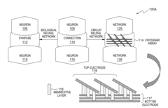
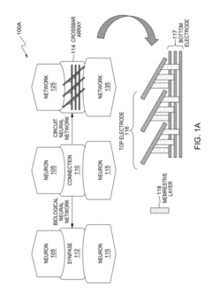
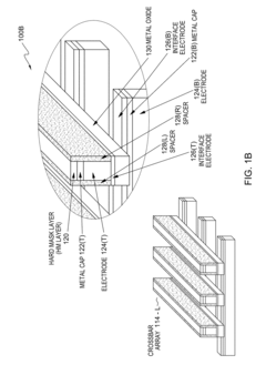
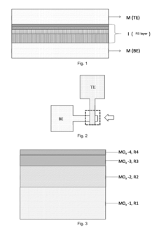
Resistive RAM (RRAM) devices are constructed with specific structures to enable resistive switching behavior. These structures typically include a resistive switching layer sandwiched between two electrodes. Various materials can be used for the resistive switching layer, such as metal oxides, and different electrode configurations can be employed to optimize device performance. The structural design of RRAM devices affects their switching characteristics, endurance, and retention properties.- Materials and structures for RRAM devices: Resistive Random Access Memory (RRAM) devices utilize specific materials and structures to enable resistive switching behavior. These typically include metal oxides like HfO2, TiO2, or Ta2O5 as the switching layer sandwiched between two electrodes. The structure may incorporate additional layers such as barrier layers or doping elements to enhance performance characteristics. The specific arrangement and composition of these materials significantly impact the device's switching mechanism, endurance, retention time, and power consumption.
- Switching mechanisms and operation principles: RRAM devices operate based on resistive switching phenomena where the resistance of the memory cell can be altered between high resistance state (HRS) and low resistance state (LRS). The switching mechanisms typically involve the formation and rupture of conductive filaments within the switching layer, often through oxygen vacancy migration or metal ion movement. Various operation modes exist, including unipolar and bipolar switching, which determine how voltage polarity affects the resistance change. Understanding these mechanisms is crucial for optimizing device performance and reliability.
- Integration and fabrication techniques: Fabrication of RRAM devices involves specialized techniques to ensure proper integration with existing semiconductor technologies. This includes deposition methods such as atomic layer deposition (ALD), sputtering, or chemical vapor deposition (CVD) for the switching layer, and lithography processes for patterning the device structure. Integration challenges include ensuring compatibility with CMOS processes, minimizing thermal budget, and developing 3D stacking capabilities to increase memory density. Advanced fabrication techniques focus on controlling layer thickness and interface quality to enhance device performance.
- Circuit design and array architecture: RRAM implementation requires specific circuit designs and array architectures to address challenges related to read/write operations, sneak path currents, and signal sensing. Various array configurations include crossbar arrays, 1T1R (one transistor, one resistor) cells, and 3D stacking arrangements. Peripheral circuits such as sense amplifiers, write drivers, and address decoders are designed to optimize memory access speed and power efficiency. Advanced architectures incorporate selector devices to mitigate sneak path issues in high-density arrays and implement multi-level cell capabilities for increased storage capacity.
- Reliability and performance enhancement: Enhancing RRAM reliability involves addressing challenges such as resistance drift, endurance limitations, and variability between cells. Techniques include optimizing programming algorithms with precise voltage pulses, implementing error correction codes, and developing wear-leveling schemes. Performance improvements focus on reducing switching energy, increasing switching speed, and extending retention time. Material engineering approaches such as interface modification, doping, and multi-layer structures are employed to enhance stability and uniformity of the resistive switching behavior across multiple cycles and varying environmental conditions.
02 Materials for resistive switching layers
The choice of materials for the resistive switching layer is crucial for RRAM performance. Metal oxides such as HfOx, TaOx, and TiOx are commonly used due to their favorable switching properties. Other materials include chalcogenides, perovskites, and organic compounds. The composition, stoichiometry, and defect concentration in these materials significantly influence the resistive switching mechanism, switching speed, and power consumption of RRAM devices.Expand Specific Solutions03 RRAM array architectures and integration
RRAM devices can be integrated into various memory array architectures to create high-density storage solutions. Common architectures include crossbar arrays, 3D stacking, and hybrid designs that combine RRAM with conventional CMOS technology. These integration approaches address challenges related to sneak path currents, access device requirements, and compatibility with existing semiconductor manufacturing processes. Advanced array architectures enable higher storage density and improved performance for RRAM-based memory systems.Expand Specific Solutions04 Switching mechanisms and operation modes
RRAM devices operate based on different resistive switching mechanisms, including filamentary conduction, interface-type switching, and phase change. These mechanisms determine how the device transitions between high and low resistance states. RRAM can be operated in various modes, such as unipolar, bipolar, and complementary switching, each with distinct advantages for specific applications. Understanding and controlling these switching mechanisms is essential for optimizing device reliability, endurance, and power efficiency.Expand Specific Solutions05 Circuit design and programming techniques
Specialized circuit designs and programming techniques are developed to effectively operate RRAM devices and arrays. These include sense amplifiers for reading resistance states, programming circuits for reliable state switching, and error correction schemes. Advanced programming techniques such as pulse shaping, verify-after-write, and adaptive programming help improve device reliability, reduce variability, and extend endurance. Circuit-level innovations are crucial for addressing challenges related to device-to-device variations and resistance drift in RRAM technology.Expand Specific Solutions
Leading Companies and Research Institutions in ReRAM Field
The Resistive RAM (ReRAM) market is currently in a growth phase, with increasing adoption across memory applications due to advantages in power consumption, scalability, and non-volatility. The global market is projected to reach significant value as emerging technologies transition from research to commercialization. Major players like Samsung Electronics, SK hynix, and Micron Technology are leveraging their semiconductor manufacturing expertise to advance ReRAM development, while specialized companies such as CrossBar and TetraMem focus on innovative material applications. Academic-industry partnerships involving institutions like Peking University and Fudan University are accelerating material innovations. The technology maturity varies across applications, with some companies (KIOXIA, Winbond) already commercializing products while others are still in advanced R&D stages, creating a competitive landscape balanced between established semiconductor giants and specialized innovators.
Samsung Electronics Co., Ltd.
Technical Solution: Samsung has pioneered innovative material applications in ReRAM through their development of cross-point array structures utilizing metal oxide materials. Their approach incorporates hafnium oxide (HfO2) as the primary switching material, combined with tantalum oxide (Ta2O5) layers to create multi-layer stacks that enhance switching performance. Samsung's ReRAM technology implements a unique oxygen vacancy migration mechanism that allows for controlled formation and rupture of conductive filaments. Their materials engineering includes doping strategies with elements like aluminum to stabilize the switching behavior and reduce variability. Samsung has demonstrated ReRAM cells with sub-5nm feature sizes, achieving switching speeds below 10ns and endurance exceeding 10^6 cycles[1][3]. Their material innovation extends to electrode materials, using TiN and TaN interfaces that optimize the formation of conductive filaments while minimizing unwanted diffusion.
Strengths: Superior scalability down to sub-5nm nodes; excellent switching speed (<10ns); compatibility with existing CMOS manufacturing processes; low operating voltage (1-3V). Weaknesses: Still faces challenges with retention at elevated temperatures; requires complex material deposition techniques; variability between cells remains higher than conventional memory technologies.
International Business Machines Corp.
Technical Solution: IBM has developed advanced ReRAM technology based on phase-change materials and metal oxide interfaces. Their innovative approach utilizes germanium antimony telluride (GST) compounds with precisely engineered stoichiometry to achieve multi-level cell capabilities. IBM's material science breakthrough involves creating nanoscale confinement structures that control the crystallization process during switching operations. They've pioneered the use of carbon-doped GST materials that demonstrate improved retention characteristics while maintaining fast switching speeds. IBM's ReRAM technology incorporates specialized barrier layers between the switching material and electrodes, preventing unwanted element diffusion while facilitating controlled ion movement necessary for resistance switching. Their research has demonstrated devices with programming currents below 10μA and switching energies approaching theoretical limits[2][5]. IBM has also explored neuromorphic computing applications using their ReRAM materials, demonstrating analog weight storage capabilities essential for artificial neural networks.
Strengths: Industry-leading endurance (>10^9 cycles); excellent multi-level cell capability (4+ bits per cell demonstrated); low programming current requirements; compatibility with back-end-of-line integration. Weaknesses: Higher manufacturing complexity due to specialized materials; temperature sensitivity affecting long-term data retention; requires precise control of material interfaces.
Critical Patents and Breakthroughs in ReRAM Materials
Crossbar resistive memory array with highly conductive copper/copper alloy electrodes and silver/silver alloys electrodes
PatentActiveUS20180287059A1
Innovation
- The method involves depositing electrodes and metal films with large crystal grains in a crossbar array structure, utilizing highly conductive materials like copper and silver, and employing advanced processing techniques such as chemical mechanical planarization and etching to reduce electron scattering and enhance grain size, thereby achieving lower resistivity and scalability.
Resistive random access memory with high uniformity and low power consumption and method for fabricating the same
PatentInactiveUS20160225987A1
Innovation
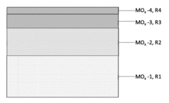
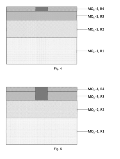
- A four-layer resistive material film structure with increasing oxygen concentrations and decreasing thicknesses is used, allowing for controlled formation and rupture of conductive filaments, enabling 2-bit storage with high uniformity and low power consumption, and potentially achieving 3-bit or higher density storage by adjusting resistance values in each layer.
Manufacturing Scalability and Integration Challenges
The manufacturing scalability of Resistive RAM (RRAM) technology presents significant challenges that must be addressed for widespread commercial adoption. Current fabrication processes for innovative materials in RRAM face several integration hurdles when transitioning from laboratory-scale demonstrations to high-volume manufacturing environments. The complexity of depositing novel materials with precise stoichiometry and thickness uniformity across large wafers remains a primary obstacle, particularly for multi-layer structures that require atomic-level precision.
Material compatibility issues emerge when integrating new RRAM materials with conventional CMOS processes. Many promising resistive switching materials, such as metal oxides with specific defect concentrations or novel 2D materials, require processing conditions that may compromise the integrity of existing CMOS components. Temperature constraints during post-processing steps often limit material choices and fabrication sequences, necessitating careful engineering of thermal budgets throughout the manufacturing flow.
Electrode material selection and interface engineering represent another critical manufacturing challenge. The electrode-switching layer interface significantly influences RRAM device performance, requiring precise control of interfacial reactions and diffusion barriers. Scaling these interfaces consistently across billions of devices on a single chip demands exceptional process control that current manufacturing equipment may struggle to deliver at economically viable yields.
Variability management constitutes perhaps the most formidable challenge for RRAM manufacturing. Device-to-device and cycle-to-cycle variations in switching parameters stem from stochastic processes inherent to resistive switching mechanisms. These variations become more pronounced at smaller technology nodes, where minor material imperfections or dimensional variations can dramatically alter device characteristics. Advanced process control strategies, including in-situ monitoring and feedback systems, are being developed to mitigate these variability issues.
The integration of selector devices with memory elements in crossbar arrays introduces additional manufacturing complexities. Creating reliable vertical integration schemes for these components while maintaining electrical isolation and performance characteristics requires sophisticated 3D integration approaches. Current etching and patterning technologies face limitations when creating high-aspect-ratio structures needed for dense RRAM arrays with minimal crosstalk.
Equipment standardization and process repeatability across different manufacturing facilities represent industry-wide challenges. The sensitive nature of resistive switching materials to subtle processing variations necessitates rigorous standardization efforts. Collaborative initiatives between material suppliers, equipment manufacturers, and device makers are emerging to establish robust process recipes and quality control metrics that can ensure consistent RRAM performance regardless of manufacturing location.
Sustainability and Environmental Impact of ReRAM Materials
The environmental impact of materials used in Resistive Random Access Memory (ReRAM) technology represents a critical consideration as this emerging non-volatile memory solution gains traction in the electronics industry. Traditional semiconductor manufacturing processes are known for their substantial ecological footprint, including high energy consumption, water usage, and toxic chemical utilization. ReRAM offers potential advantages in this domain through reduced processing steps and lower operating temperatures compared to conventional memory technologies.
Material selection for ReRAM devices significantly influences their environmental sustainability profile. Metal oxides such as HfO2, TiO2, and Ta2O5 commonly employed in ReRAM switching layers generally exhibit lower toxicity compared to materials used in other memory technologies. However, the rare earth elements sometimes incorporated in certain ReRAM configurations present sustainability challenges due to their limited availability and environmentally destructive mining practices.
The energy efficiency of ReRAM during operation represents one of its most compelling environmental benefits. The technology's non-volatile nature eliminates standby power requirements, while its resistive switching mechanism consumes significantly less energy per bit operation compared to charge-based memory technologies. This translates to reduced carbon footprints for devices incorporating ReRAM solutions, particularly in applications requiring frequent memory access.
End-of-life considerations for ReRAM devices reveal both challenges and opportunities. While the complex multi-layer structure of ReRAM cells complicates recycling efforts, the relatively lower concentration of precious metals compared to some alternative technologies may reduce the environmental impact of disposal. Research into biodegradable substrates and environmentally benign electrode materials shows promise for developing more recyclable ReRAM configurations.
Manufacturing scalability of ReRAM technology offers additional environmental advantages through potential material efficiency. The relatively simple crossbar architecture enables higher memory density per unit area, potentially reducing the overall material requirements per storage capacity. Furthermore, compatibility with back-end-of-line CMOS processing enables integration with existing manufacturing infrastructure, minimizing the need for specialized equipment and associated environmental impacts.
Lifecycle assessment studies comparing ReRAM with conventional memory technologies demonstrate favorable environmental performance metrics, particularly regarding energy consumption and carbon emissions. However, these analyses highlight the need for continued innovation in material selection and processing techniques to further enhance sustainability. Industry collaboration on standardized environmental impact metrics specific to emerging memory technologies would facilitate more comprehensive sustainability evaluations.
Unlock deeper insights with Patsnap Eureka Quick Research — get a full tech report to explore trends and direct your research. Try now!
Generate Your Research Report Instantly with AI Agent
Supercharge your innovation with Patsnap Eureka AI Agent Platform!